Original Power Supply IC LNK354PN LNK354P LNK354 DIP-7 New
https://authelectronic.com/original-power-ic-lnk354pn-lnk354p-lnk354-dip-7-neworiginal-power-ic-lnk354pn-lnk354p-lnk354-dip-7-new
Call Girls Walvekar Nagar Call Me 7737669865 Budget Friendly No Advance Booking
Original Power Supply IC LNK354PN LNK354P LNK354 DIP-7 New
1. LNK353/354
LinkSwitch-HF Family
Enhanced, Energy Efficient, Low Power
Off-Line Switcher IC
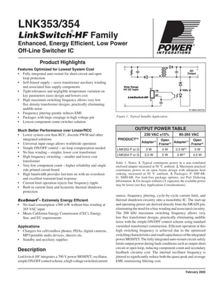
Figure 1. Typical Standby Application.
Product Highlights
Features Optimized for Lowest System Cost
• Fully integrated auto-restart for short-circuit and open
loop protection
• Self-biased supply – saves transformer auxiliary winding
and associated bias supply components
• Tight tolerances and negligible temperature variation on
key parameters eases design and lowers cost
• High maximum switching frequency allows very low
flux density transformer designs, practically eliminating
audible noise
• Frequency jittering greatly reduces EMI
• Packages with large creepage to high voltage pin
• Lowest component count switcher solution
Much Better Performance over Linear/RCC
• Lower system cost than RCC, discrete PWM and other
integrated solutions
• Universal input range allows worldwide operation
• Simple ON/OFF control – no loop compensation needed
• No bias winding – simpler, lower cost transformer
• High frequency switching – smaller and lower cost
transformer
• Very low component count – higher reliability and single
side printed circuit board
• High bandwidth provides fast turn on with no overshoot
and excellent transient load response
• Current limit operation rejects line frequency ripple
• Built-in current limit and hysteretic thermal shutdown
protection
EcoSmart
®
– Extremely Energy Efficient
• No-load consumption <300 mW without bias winding at
265 VAC input
• Meets California Energy Commission (CEC), Energy
Star, and EU requirements
Applications
• Chargers for cell/cordless phones, PDAs, digital cameras,
MP3/portable audio devices, shavers etc.
• Standby and auxiliary supplies
Description
LinkSwitch-HF integrates a 700 V power MOSFET, oscillator,
simpleON/OFFcontrolscheme,ahighvoltageswitchedcurrent
®
Table 1. Notes: 1. Typical continuous power in a non-ventilated
enclosed adapter measured at 50 °C ambient. 2. Maximum practical
continuous power in an open frame design with adequate heat
sinking, measured at 50 °C ambient. 3. Packages: P: DIP-8B,
G: SMD-8B. For lead-free package options, see Part Ordering
Information. 4. For designs without aYcapacitor, the available power
may be lower (see Key Applications Considerations).
source, frequency jittering, cycle-by-cycle current limit, and
thermal shutdown circuitry onto a monolithic IC. The start-up
and operating power are derived directly from the DRAIN pin,
eliminatingtheneedforabiaswindingandassociatedcircuitry.
The 200 kHz maximum switching frequency allows very
low flux transformer designs, practically eliminating audible
noise with the simple ON/OFF control scheme using standard
varnished transformer construction. Efficient operation at this
high switching frequency is achieved due to the optimized
switchingcharacteristicsandsmallcapacitancesoftheintegrated
power MOSFET.The fully integratedauto-restart circuit safely
limits output power during fault conditions such as output short
circuit or open loop, reducing component count and secondary
feedback circuitry cost. The internal oscillator frequency is
jittered to significantly reduce both the quasi-peak and average
EMI, minimizing filtering cost.
DC
Output
Wide Range
HV DC Input
PI-3855-022704
+ +
LinkSwitch-HF
D
S
BP
FB
February 2005
OUTPUT POWER TABLE
PRODUCT(3)
230 VAC ±15% 85-265 VAC
Adapter(1) Open
Frame(2) Adapter(1) Open
Frame(2)
LNK353 P or G 3 W 4 W 2.5 W(4)
3 W
LNK354 P or G 3.5 W 5 W 3 W(4)
4.5 W
2. LNK353/354
F
2/052
PI-2367-021105
CLOCK
JITTER
OSCILLATOR
5.8 V
4.85 V
SOURCE
(S)
S
R
Q
DCMAX
BYPASS
(BP)
FAULT
PRESENT
+
- VILIMIT
LEADING
EDGE
BLANKING
THERMAL
SHUTDOWN
+
-
DRAIN
(D)
REGULATOR
5.8 V
BYPASS PIN
UNDER-VOLTAGE
CURRENT LIMIT
COMPARATOR
FEEDBACK
(FB)
Q
6.3 V
RESET
AUTO-
RESTART
COUNTER
1.65 V -VT
CLOCK
Figure 3. Pin Configuration.
Pin Functional Description
DRAIN (D) Pin:
Power MOSFET drain connection. Provides internal operating
current for both start-up and steady-state operation.
BYPASS (BP) Pin:
Connection point for a 0.1 µF external bypass capacitor for the
internally generated 5.8 V supply.
FEEDBACK (FB) Pin:
During normal operation, switching of the power MOSFET is
controlled by this pin. MOSFET switching is terminated when
a current greater than 49 µA is delivered into this pin.
SOURCE (S) Pin:
This pin is the power MOSFET source connection. It is also the
ground reference for the BYPASS and FEEDBACK pins.
PI-3491-111903
FB D
S
BP
S
SS
P Package (DIP-8B)
G Package (SMD-8B)
8
5
7
1
4
2
3
Figure 2. Functional Block Diagram.
3. LNK353/354
F
2/05 3
PI-3857-022504
0 6.4
Time (µs)
0
100
200
400
500
600
300
V
DRAIN
208 kHz
192 kHz
LinkSwitch-HF Functional
Description
LinkSwitch-HF combines a high voltage power MOSFET
switch with a power supply controller in one device. Unlike
conventional PWM (pulse width modulator) controllers,
LinkSwitch-HF uses a simple ON/OFF control to regulate the
output voltage. The LinkSwitch-HF controller consists of an
oscillator, feedback (sense and logic) circuit, 5.8 V regulator,
BYPASSpinunder-voltagecircuit,over-temperatureprotection,
frequency jittering, current limit circuit, leading edge blanking
and a 700Vpower MOSFET.The LinkSwitch-HF incorporates
additional circuitry for auto-restart.
Oscillator
The typical oscillator frequency is internally set to an average
of 200 kHz. Two signals are generated from the oscillator: the
maximum duty cycle signal (DCMAX
) and the clock signal that
indicates the beginning of each cycle.
The LinkSwitch-HF oscillator incorporates circuitry that
introduces a small amount of frequency jitter, typically 16 kHz
peak-to-peak,tominimizeEMIemission.Themodulationrateof
the frequency jitter is set to 1.5 kHz to optimize EMI reduction
for both average and quasi-peak emissions. The frequency
jitter should be measured with the oscilloscope triggered at
the falling edge of the DRAIN waveform. The waveform in
Figure 4 illustrates the frequency jitter of the LinkSwitch-HF.
Feedback Input Circuit
The feedback input circuit at the FB pin consists of a low
impedancesourcefolloweroutputsetat1.65V.Whenthecurrent
deliveredintothispinexceeds49µA,alowlogiclevel(disable)
is generated at the output of the feedback circuit. This output
is sampled at the beginning of each cycle on the rising edge of
the clock signal. If high, the power MOSFET is turned on for
thatcycle(enabled),otherwisethepowerMOSFETremainsoff
(disabled). Since the sampling is done only at the beginning of
each cycle, subsequent changes in the FB pin voltage or current
during the remainder of the cycle are ignored.
5.8 V Regulator and 6.3 V Shunt Voltage Clamp
The 5.8 V regulator charges the bypass capacitor connected
to the BYPASS pin to 5.8 V by drawing a current from the
voltage on the DRAIN, whenever the MOSFET is off. The
BYPASS pin is the internal supply voltage node for the
LinkSwitch-HF. When the MOSFET is on, the LinkSwitch-HF
runs off of the energy stored in the bypass capacitor. Extremely
low power consumption of the internal circuitry allows the
LinkSwitch-HF to operate continuously from the current drawn
fromtheDRAINpin.Abypasscapacitorvalueof0.1µFissufficient
for both high frequency decoupling and energy storage.
In addition, there is a 6.3 V shunt regulator clamping the
BYPASS pin at 6.3 V when current is provided to the BYPASS
pin through an external resistor. This facilitates powering of
LinkSwitch-HF externally through a bias winding to decrease
the no-load consumption to less than 50 mW.
BYPASS Pin Under-Voltage
The BYPASS pin under-voltage circuitry disables the power
MOSFET when the BYPASS pin voltage drops below 4.85 V.
Once the BYPASS pin voltage drops below 4.85 V, it must rise
back to 5.8 V to enable (turn-on) the power MOSFET.
Over-Temperature Protection
The thermal shutdown circuitry senses the die temperature.
The threshold is set at 142 °C typical with a 75 °C hysteresis.
Whenthedietemperaturerisesabovethisthreshold(142°C)the
power MOSFET is disabled and remains disabled until the die
temperature falls by 75 °C, at which point it is re-enabled.
Current Limit
ThecurrentlimitcircuitsensesthecurrentinthepowerMOSFET.
When this current exceeds the internal threshold (ILIMIT
), the
power MOSFET is turned off for the remainder of that cycle.
The leading edge blanking circuit inhibits the current limit
comparator for a short time (tLEB
) after the power MOSFET
is turned on. This leading edge blanking time has been set so
that current spikes caused by capacitance and rectifier reverse
recovery time will not cause premature termination of the
switching pulse.
Auto-Restart
In the event of a fault condition such as output overload, output
short circuit, or an open loop condition, LinkSwitch-HF enters
into auto-restart operation. An internal counter clocked by the
oscillator gets reset every time the FB pin is pulled high. If
the FB pin is not pulled high for 30 ms, the power MOSFET
switching is disabled for 650 ms. The auto-restart alternately
enables and disables the switching of the power MOSFET until
the fault condition is removed.
Figure 4. Frequency Jitter.
4. LNK353/354
F
2/054
Applications Example
A 2.4 W CC/CV Charger Adapter
The circuit shown in Figure 5 is a typical implementation of
a 5.7 V, 400 mA, constant voltage, constant current (CV/CC)
battery charger.
The input bridge formed by diodes D1-D4, rectifies the AC
input voltage. The rectified AC is then filtered by the bulk
storage capacitors C1 and C2. Resistor RF1 is a flameproof,
fusible, wire wound type and functions as a fuse, inrush current
limiter and, together with the π filter formed by C1, C2 and L1,
differential mode noise attenuator.
This simple EMI filtering, together with the frequency jittering
of LinkSwitch-HF (U1), a small value Y1 capacitor (CY1),
and shield windings within T1, and a secondary-side RC
snubber (R5, C5), allows the design to meet both conducted
and radiated EMI limits. The low value of CY1 is important
to meet the requirement of low line frequency leakage current,
in this case <10 µA.
The rectified and filtered input voltage is applied to the primary
winding of T1. The other side of the transformer primary is
driven by the integrated MOSFET in U1. Diode D5, C3, R1
and R3 form the primary clamp network. This limits the peak
drain voltage due to leakage inductance. Resistor R3 allows the
use of a slow, low cost rectifier diode by limiting the reverse
current through D5 when U1 turns on. The selection of a slow
diode improves efficiency and conducted EMI.
Output rectification is provided by Schottky diode D6. The low
forward voltage provides high efficiency across the operating
range and the low ESR capacitor C6 minimizes output voltage
ripple.
In constant voltage (CV) mode, the output voltage is set by the
ZenerdiodeVR1andtheemitter-basevoltageofPNPtransistor
Q1. The VBE
of Q1 divided by the value of R7 sets the bias
current through VR1 (~2.7 mA). When the output voltage
exceeds the threshold voltage determined by Q1 and VR1, Q1
is turned on and current flows through the LED of U2. As the
LED current increases, the current fed into the FEEDBACK
pin increases, disabling further switching cycles of U1. At
very light loads, almost all switching cycles will be disabled,
giving a low effective switching frequency and providing low
no-load consumption.
Duringloadtransients,R6andR8ensurethattheratingsofQ1are
not exceeded while R4 prevents C4 from being discharged.
Resistors R9 and R10 form the constant current (CC) sense
circuit. Above approximately 400 mA, the voltage across the
senseresistorexceedstheoptocouplerdiodeforwardconduction
voltage of approximately 1 V. The current through the LED
is therefore determined by the output current and CC control
dominatesovertheCVfeedbackloop.CCcontrolismaintained
even under output short circuit conditions.
D
S
FB
BP
RF1
8.2 Ω
2.5 W
85-265
VAC
5.7 V,
400 mA
J3-2
RTN
J3-1
J1
J2
R3
200 Ω
R5
68 ΩR1
100 kΩ
R4
5.1 kΩ
R6
6.8 Ω
R9
200 Ω
R10
2.4 Ω
1 W
R8
390 Ω
U2A
PC817D
VR1
BZX79B5V1
5.1 V, 2%
R7
220 Ω
U2B
PC817D
D1
1N4005
D2
1N4005
D5
1N4007GP
D3
1N4005
D4
1N4005
D6
SS14
C6
330 µF
16 V
Q1
MMST
3906
L1
1 mH
CY1
100 pF
C1
4.7 µF
400 V
C3
2.2 nF
400 V
5
3
4 5 9
8
T1
EE16
NC NC
U1
LNK354P
C2
4.7 µF
400 V
C4
100 nF
C5
2.2 nF
LinkSwitch-HF
PI-3891-070204
Figure 5. Universal Input, 5.7 V, 400 mA, Constant Voltage, Constant Current Battery Charger Using LinkSwitch-HF.
5. LNK353/354
F
2/05 5
Key Application Considerations
LinkSwitch-HF Design Considerations
Output Power Table
Data sheet maximum output power table (Table 1) represents
the maximum practical continuous output power level that can
be obtained under the following assumed conditions:
1. TheminimumDCinputvoltageis90Vorhigherfor85VAC
input, or 240 V or higher for 230 VAC input or 115 VAC
with a voltage doubler. The value of the input capacitance
should be large enough to meet these criteria for AC input
designs.
2. Secondary output of 5.5 V with a Schottky rectifier diode.
3. Assumed efficiency of 70%.
4. Operating frequency of fOSC(min)
and ILIMIT(min)
.
5. Voltage only output (no secondary side constant current
circuit).
6. Continuous mode operation (0.6 ≤ KP
≤ 1).
7. The part is board mounted with SOURCE pins soldered
to a sufficient area of copper to keep the SOURCE pin
temperature at or below 100 °C.
8. Ambient temperature of 50 °C for open frame designs
and an internal enclosure temperature of 60 °C for adapter
designs.
Below a value of 1, KP
is the ratio of ripple to peak primary
current.Above a value of 1, KP
is the ratio of primary MOSFET
off time to the secondary diode conduction time.
Operatingatalowereffectiveswitchingfrequencycansimplify
meeting conducted and radiated EMI limits, especially for
designs where the safety Y capacitor must be eliminated. By
using a lower effective full load frequency, the calculated
value of the primary inductance is higher than required for
power delivery. However, the maximum power capability at
this lower operating frequency will be lower than the values
shown in Table 1.
Audible Noise
The cycle skipping mode of operation used in LinkSwitch-HF
can generate audio frequency components in the transformer.
To limit this audible noise generation, the transformer should
be designed such that the peak core flux density is below
1250 Gauss (125 mT). Following this guideline and using the
standard transformer production technique of dip varnishing
practically eliminates audible noise. Higher flux densities
are possible however, careful evaluation of the audible noise
performance should be made using production transformer
samples before approving the design.
Ceramic capacitors that use dielectrics such as Z5U, when used
in clamp circuits, may also generate audio noise. If this is the
case, try replacing them with a capacitor having a different
dielectric, for example a polyester film type.
LinkSwitch-HF Layout Considerations
See Figure 6 for a recommended circuit board layout for
LinkSwitch-HF.
Single Point Grounding
Use a single point ground connection from the input filter
capacitor to the area of copper connected to the SOURCE
pins.
Bypass Capacitor (CBP
)
TheBYPASSpincapacitorshouldbelocatedasnearaspossible
to the BYPASS and SOURCE pins.
Primary Loop Area
The area of the primary loop that connects the input filter
capacitor, transformer primary and LinkSwitch-HF together
should be kept as small as possible.
Primary Clamp Circuit
Aclamp is used to limit peak voltage on the DRAIN pin at turn
off. This can be achieved by using an RCD clamp (as shown
in Figure 5) or a Zener (~200 V) and diode clamp across the
primary winding. In all cases, to minimize EMI, care should be
taken to minimize the circuit path from the clamp components
to the transformer and LinkSwitch-HF.
Thermal Considerations
The copper area underneath the LinkSwitch-HF acts not only
as a single point ground, but also as a heatsink. As this area is
connectedtothequietsourcenode,thisareashouldbemaximized
for good heatsinking of LinkSwitch-HF. The same applies to
the cathode of the output diode.
Y-Capacitor
The placement of the Y-capacitor should be directly from
the primary input filter capacitor positive terminal to the
common/return terminal of the transformer secondary. Such
a placement will route high magnitude common mode surge
currents away from the LinkSwitch-HF device. Note that if an
input π (C, L, C) EMI filter is used, then the inductor in the
filter should be placed between the negative terminals of the
input filter capacitors.
Optocoupler
Place the optocoupler physically close to the LinkSwitch-HF to
minimize the primary side trace lengths. Keep the high current,
high voltage drain and clamp traces away from the optocoupler
to prevent noise pick up.
Output Diode
For best performance, the area of the loop connecting the
secondary winding, the output diode and the output filter
capacitor should be minimized. In addition, sufficient copper
area should be provided at the anode and cathode terminals
6. LNK353/354
F
2/056
of the diode for heatsinking. A larger area is preferred at the
quiet cathode terminal. A large anode area can increase high
frequency radiated EMI.
Quick Design Checklist
As with any power supply design, all LinkSwitch-HF designs
should be verified on the bench to make sure that component
specificationsarenotexceededunderworst-caseconditions.The
following minimum set of tests is strongly recommended:
1. Maximum drain voltage – Verify that VDS
does not exceed
675Vatthehighestinputvoltageandpeak(overload)output
power.
2. Maximumdraincurrent–Atmaximumambienttemperature,
maximum input voltage and peak output (overload) power,
verify drain current waveforms for any signs of transformer
saturation and excessive leading edge current spikes at
startup. Repeat under steady state conditions and verify that
Figure 6. Recommended Printed Circuit Layout for LinkSwitch-HF in a Flyback Converter Configuration.
the leading edge current spike event is below ILIMIT(MIN)
at the
endofthetLEB(MIN)
.Underallconditions,themaximumdrain
current should be below the specified absolute maximum
ratings.
3. Thermal Check – At specified maximum output power,
minimuminputvoltageandmaximumambienttemperature,
verify that the temperature specifications are not exceeded
for LinkSwitch-HF, transformer, output diode, and output
capacitors. Enough thermal margin should be allowed for
part-to-part variation of the RDS(ON)
of LinkSwitch-HF as
specifiedinthedatasheet.Underlowline,maximumpower,
a maximum LinkSwitch-HF SOURCE pin temperature of
100 °C is recommended to allow for these variations.
Design Tools
Up-to-date information on design tools can be found at the
Power Integrations website: www.powerint.com.
+HV DC
Input
PI-3890-102704
Input Filter
Capacitor
CBP
-
DC
Out
Output Filter
Capacitor
Y1-
Capacitor
Maximize hatched copper
areas ( ) for optimum
heatsinking
TOP VIEW
DS
S BP FBS
S
LinkSwitch-HF
+
-
Opto-
coupler
PRI SEC
T
r
a
n
s
f
o
r
m
e
r
7. LNK353/354
F
2/05 7
ABSOLUTE MAXIMUM RATINGS(1,5)
DRAIN Voltage ..................................................-0.3Vto700V
PeakDRAINCurrent......................................400mA (750mA)(2)
FEEDBACKVoltage................................................-0.3Vto9V
FEEDBACK Current .................................................... 100 mA
BYPASSVoltage......................................................-0.3Vto9V
StorageTemperature..........................................-65°C to150°C
OperatingJunctionTemperature(3)
.....................-40°C to150°C
LeadTemperature(4)
..........................................................260°C
Notes:
1. All voltages referenced to SOURCE, TA
= 25 °C.
2. The higher peak DRAIN current is allowed while the
DRAIN voltage is less than 400 V.
3. Normally limited by internal circuitry.
4. 1/16 in. from case for 5 seconds.
5. Maximum ratings specified may be applied, one at a time,
without causing permanent damage to the product.
Exposure to Absolute Maximum Rating conditions for
extended periods of time may affect product reliability.
THERMAL IMPEDANCE
Thermal Impedance: P or G Package:
(θJA
) ........................... 70 °C/W(2)
; 60 °C/W(3)
(θJC
)(1)
............................................... 11 °C/W
Notes:
1. Measured on pin 2 (SOURCE) close to plastic interface.
2. Soldered to 0.36 sq. in. (232 mm2
), 2 oz. (610 g/m2
) copper clad.
3. Soldered to 1 sq. in. (645 mm2
), 2 oz. (610 g/m2
) copper clad.
Parameter Symbol
Conditions
SOURCE = 0 V; TJ
= -40 to 125 °C
See Figure 7
(Unless Otherwise Specified)
Min Typ Max Units
CONTROL FUNCTIONS
Output Frequency fOSC
TJ
= 25 °C
Average 186 200 214
kHz
Peak-Peak Jitter 16
Maximum Duty
Cycle
DCMAX
S2 Open 60 63 %
FEEDBACK Pin
Turnoff Threshold
Current
IFB
TJ
= 25 °C 30 49 68 µA
FEEDBACK Pin
Voltage
VFB
IFB
= 49 µA 1.54 1.65 1.76 V
DRAIN Supply
Current
IS1
VFB
≥2 V
(MOSFET Not Switching)
See Note A
200 275 µA
IS2
FEEDBACK Open
(MOSFET Switching)
See Notes A, B
280 365 µA
BYPASS Pin
Charge Current
ICH1
VBP
= 0 V, TJ
= 25 °C
See Note C
-5.5 -3.3 -1.8
mA
ICH2
VBP
= 4 V, TJ
= 25 °C
See Note C
-3.8 -2.1 -1.0
BYPASS Pin
Voltage
VBP
5.55 5.8 6.10 V
BYPASS Pin
Voltage Hysteresis
VBPH
0.8 0.95 1.2 V
8. LNK353/354
F
2/058
Parameter Symbol
Conditions
SOURCE = 0 V; TJ
= -40 to 125 °C
See Figure 7
(Unless Otherwise Specified)
Min Typ Max Units
CONTROL FUNCTIONS (cont)
BYPASS Pin
Supply Current
IBPSC
See Note D 68 µA
CIRCUIT PROTECTION
Current Limit
ILIMIT
(See
Note E)
di/dt = 90 mA/µs
TJ
= 25 °C
LNK353
172 185 198
mA
di/dt = 400 mA/µs
TJ
= 25 °C
215 245 274
di/dt = 115 mA/µs
TJ
= 25 °C
LNK354
233 250 268
di/dt = 500 mA/µs
TJ
= 25 °C
264 300 336
Minimum On Time tON(MIN)
LNK353 390 470 610
ns
LNK354 280 360 500
Leading Edge
Blanking Time
tLEB
TJ
= 25 °C
See Note F
170 215 ns
Thermal
Shutdown
Temperature
TSD
135 142 150 °C
Thermal
Shutdown
Hysteresis
TSHD
See Note G 75 °C
OUTPUT
ON-State
Resistance
RDS(ON)
LNK353
ID
= 25 mA
TJ
= 25 °C 34 40
Ω
TJ
= 100 °C 54 63
LNK354
ID
= 25 mA
TJ
= 25 °C 24 28
TJ
= 100 °C 38 45
OFF-State Drain
Leakage Current
IDSS
VBP
= 6.2 V, VFB
≥2 V,
VDS
= 560 V,
TJ
= 125 °C
50 µA
Breakdown
Voltage
BVDSS
VBP
= 6.2 V, VFB
≥2 V,
TJ
= 25 °C
700 V
Rise Time tR Measured in a Typical Flyback
Converter Application
50 ns
Fall Time tF
50 ns
9. LNK353/354
F
2/05 9
Parameter Symbol
Conditions
SOURCE = 0 V; TJ
= -40 to 125 °C
See Figure 7
(Unless Otherwise Specified)
Min Typ Max Units
OUTPUT (cont)
DRAIN Supply
Voltage
50 V
Output Enable
Delay
tEN
See Figure 9 10 µs
Output Disable
Setup Time
tDST
0.5 µs
Auto-Restart
ON-Time
tAR
TJ
= 25 °C
See Note H
31 ms
Auto-Restart Duty
Cycle
DCAR
5 %
NOTES:
A. Total current consumption is the sum of IS1
and IDSS
when FEEDBACK pin voltage is ≥2 V (MOSFET not
switching) and the sum of IS2
and IDSS
when FEEDBACK pin is shorted to SOURCE (MOSFET switching).
B Since the output MOSFET is switching, it is difficult to isolate the switching current from the supply current at the
DRAIN. An alternative is to measure the BYPASS pin current at 6 V.
C. See Typical Performance Characteristics section Figure 14 for BYPASS pin start-up charging waveform.
D. This current is only intended to supply an optional optocoupler connected between the BYPASS and FEEDBACK
pins and not any other external circuitry.
E. For current limit at other di/dt values, refer to Figure 13.
F. This parameter is guaranteed by design.
G. This parameter is derived from characterization.
H. Auto-restart on time has the same temperature characteristics as the oscillator (inversely proportional to
frequency).
10. LNK353/354
F
2/0510
Figure 7. LinkSwitch-HF General Test Circuit.
PI-3490-060204
50 V50 V
D FB
SS
S S
BP
S1
470 kΩ
S2
0.1 µF
470 Ω
5 W
PI-2048-033001
DRAIN
VOLTAGE
HV
0 V
90%
10%
90%
t2
t1
D =
t1
t2
PI-3707-112503
FB
tP
tEN
DCMAX
t
P
=
1
fOSC
VDRAIN
(internal signal)
Figure 8. LinkSwitch-HF Duty Cycle Measurement. Figure 9. LinkSwitch-HF Output Enable Timing.
11. LNK353/354
F
2/05 11
200
300
350
400
250
0
0 42 86 10 12 14 16 18 20
DRAIN Voltage (V)
DRAINCurrent(mA)
PI-3949-102004
50
150
100
25 °C
100 °C
Scaling Factors:
LNK353 0.7
LNK354 1.0
Typical Performance Characteristics
Figure 14. BYPASS Pin Start-up Waveform.
1.1
1.0
0.9
-50 -25 0 25 50 75 100 125 150
Junction Temperature (°C)
BreakdownVoltage
(Normalizedto25°C)
PI-2213-012301
6
5
4
3
2
1
0
0 0.2 0.4 0.6 0.8 1.0
Time (ms)
PI-2240-012301
BYPASSPinVoltage(V)
7
Figure 10. Breakdown vs. Temperature.
Figure 12. Current Limit vs. Temperature at
Normalized di/dt.
Figure 13. Current Limit vs. di/dt.
Figure 15. Output Characteristics.
Figure 11. Frequency vs. Temperature.
TBD
Temperature (°C)
PI-3709-111203
CurrentLimit
(Normalizedto25°C)
1.0
1.2
1.4
0.8
0.6
0.4
0.2
0
-50 0 50 100 150
di/dt = 1
di/dt = 6
Normalized di/dt
1.2
1.0
0.8
0.6
0.4
0.2
0
-50 -25 0 25 50 75 100 125
Junction Temperature (°C)
PI-2680-012301
OutputFrequency
(Normalizedto25°C)
Normalized di/dt
PI-3892-061604
NormalizedCurrentLimit
1.0
1.2
1.4
0.8
0.6
0.4
0.2
0
1 2 3 4 5
LNK353
LNK354
LNK353
LNK354
Normalized
di/dt = 1
90 mA/µs
115 mA/µs
Normalized
Current
Limit = 1
185 mA
250 mA
12. LNK353/354
F
2/0512
Drain Voltage (V)
DrainCapacitance(pF)
PI-3888-052104
0 100 200 300 400 500 600
1
10
100
1000
Figure 16. COSS
vs. Drain Voltage.
Typical Performance Characteristics (cont.)
PART ORDERING INFORMATION
LinkSwitch Product Family
HF Series Number
Package Identifier
G Plastic Surface Mount DIP
P Plastic DIP
Lead Finish
Blank Standard (Sn Pb)
N Pure Matte Tin (Pb-Free)
Tape & Reel and Other Options
Blank Standard Configurations
TL Tape & Reel, 1 k pcs minimum, G Package onlyLNK 354 G N - TL
13. LNK353/354
F
2/05 13
Notes:
1. Package dimensions conform to JEDEC specification
MS-001-AB (Issue B 7/85) for standard dual-in-line (DIP)
package with .300 inch row spacing.
2. Controlling dimensions are inches. Millimeter sizes are
shown in parentheses.
3. Dimensions shown do not include mold flash or other
protrusions. Mold flash or protrusions shall not exceed
.006 (.15) on any side.
4. Pin locations start with Pin 1, and continue counter-clock-
wise to Pin 8 when viewed from the top. The notch and/or
dimple are aids in locating Pin 1. Pin 6 is omitted.
5. Minimum metal to metal spacing at the package body for
the omitted lead location is .137 inch (3.48 mm).
6. Lead width measured at package body.
7. Lead spacing measured with the leads constrained to be
perpendicular to plane T.
.008 (.20)
.015 (.38)
.300 (7.62) BSC
(NOTE 7)
.300 (7.62)
.390 (9.91)
.367 (9.32)
.387 (9.83)
.240 (6.10)
.260 (6.60)
.125 (3.18)
.145 (3.68)
.057 (1.45)
.068 (1.73)
.120 (3.05)
.140 (3.56)
.015 (.38)
MINIMUM
.048 (1.22)
.053 (1.35)
.100 (2.54) BSC
.014 (.36)
.022 (.56)
-E-
Pin 1
SEATING
PLANE
-D-
-T-
P08B
DIP-8B
PI-2551-121504
D S .004 (.10)⊕
T E D S .010 (.25) M⊕
(NOTE 6)
.137 (3.48)
MINIMUM
SMD-8B
PI-2546-121504
.004 (.10)
.012 (.30)
.036 (0.91)
.044 (1.12)
.004 (.10)
0 -° 8°
.367 (9.32)
.387 (9.83)
.048 (1.22)
.009 (.23)
.053 (1.35)
.032 (.81)
.037 (.94)
.125 (3.18)
.145 (3.68)
-D-
Notes:
1. Controlling dimensions are
inches. Millimeter sizes are
shown in parentheses.
2. Dimensions shown do not
include mold flash or other
protrusions. Mold flash or
protrusions shall not exceed
.006 (.15) on any side.
3. Pin locations start with Pin 1,
and continue counter-clock-
wise to Pin 8 when viewed
from the top. Pin 6 is omitted.
4. Minimum metal to metal
spacing at the package body
for the omitted lead location
is .137 inch (3.48 mm).
5. Lead width measured at
package body.
6. D and E are referenced
datums on the package
body.
.057 (1.45)
.068 (1.73)
(NOTE 5)
E S
.100 (2.54) (BSC)
.372 (9.45)
.240 (6.10)
.388 (9.86)
.137 (3.48)
MINIMUM
.260 (6.60)
.010 (.25)
-E-
Pin 1
D S .004 (.10)⊕
⊕
G08B
.420
.046 .060 .060 .046
.080
Pin 1
.086
.186
.286
Solder Pad Dimensions