This document discusses Intel's efforts to transition to environmentally green microelectronic packaging solutions through lead-free and halogen-free materials and processes. Specifically:
1) Intel has successfully transitioned to lead-free solders for first-level interconnects (connecting die to substrate), second-level interconnects (connecting substrate to board), and solder thermal interface materials. This required developing new lead-free solders, fluxes, underfills, and substrate materials compatible with higher processing temperatures.
2) Transitioning to lead-free second-level interconnects posed challenges due to higher reflow temperatures and stiffer solders, but Intel addressed reliability concerns through testing and design rules.
3)
![Materials Technology for Environmentally Green Micro-electronic Packaging 1
Materials Technology for Environmentally Green
Micro-electronic Packaging
Mukul P. Renavikar, Technology and Manufacturing Group, Intel Corporation
Neha Patel, Technology and Manufacturing Group, Intel Corporation
Ashay Dani, Technology and Manufacturing Group, Intel Corporation
Vijay Wakharkar, Technology and Manufacturing Group, Intel Corporation
George Arrigotti, Technology and Manufacturing Group, Intel Corporation
Vasu Vasudevan, Technology and Manufacturing Group, Intel Corporation
Omar Bchir, Technology and Manufacturing Group, Intel Corporation
Amruthavalli P. Alur, Technology and Manufacturing Group, Intel Corporation
Charan K. Gurumurthy, Technology and Manufacturing Group, Intel Corporation
Roger W. Stage, Technology and Manufacturing Group, Intel Corporation
Index words: Pb-free, halogen-free, solder materials, thermal interface materials, package and board
reliability, BGA, substrates, micro-electronic packaging, EU RoHS, C4
ABSTRACT
Intel has been continuously striving to provide
environmentally green micro-electronic packaging
solutions for high-density interconnect (HDI) product
applications. The environmentally green initiative
consisted of providing lead-free (Pb-free) packaging
materials solutions as well the enabling of halogen-free
(HF) substrates technology to eliminate the use of
brominated flame retardants. This paper discusses the
challenges overcome by Intel to deliver on both aspects of
environmentally green packaging. Although Intel’s efforts
to enable Pb-free and HF-compliant packaging solutions
have been wide-ranging, the scope of this paper is limited
to discussing the key technology development challenges
faced in transitioning to Pb-free materials in first-level
interconnects (FLI), second-level interconnects (2LI),
solder thermal interface materials (STIM) applications,
and halogen-free (HF) substrate materials. The transition
to Pb-free micro-electronic packaging materials and HF
substrate technology required a paradigm shift in the
industry, needing extensive benchmarking initiatives and
sharing cross-technology learnings across the industry and
academia. The delivery of Pb-free packaging solutions
across FLI, 2LI, and STIM applications as well as HF
substrate technology has strongly reinforced Intel’s One
Generation Ahead (OGA) philosophy in micro-electronic
packaging.
INTRODUCTION
Intel’s drive to “get the lead out of the package” began
over five years ago when we produced a Pb-free tin-silver-
copper (SAC) solder for 2LI applications that complied
with European Union Restriction of Hazardous
Substances (EU RoHS) requirements. Continuing on this
path to deliver “Pb-free” packaging, Intel recently reached
a critical milestone by eliminating Lead (Pb) from the FLI
solders in its next-generation 45nm Silicon technology
roadmap products. Intel is among the first semiconductor
companies to deliver Pb-free FLI solutions in high-volume
manufacturing. In order to meet the stringent integration
challenges of transitioning to Pb-free-compliant packages,
Intel has also successfully developed substrate, FLI flux,
and underfill (UF) materials technologies that are
compliant with higher Pb-free processing temperatures.
Intel has been working with suppliers, customers, and
several industry consortia to develop and provide EU
RoHS-compliant products. Intel has completed
certification of EU RoHS-compliant materials and
processes and is manufacturing and shipping many EU
RoHS-compliant products today. Additionally, in
anticipation of the RoHS regulations, Intel pro-actively
worked to develop pioneering Pb-free STIM materials to
Referência [4]](https://image.slidesharecdn.com/fbd9d1a0-b430-44e6-ab7f-1ac4ccb2c050-160416030809/85/Renavikar-IATTJ-2008-Green-Materials-for-Packaging-1-320.jpg)
![Materials Technology for Environmentally Green Micro-electronic Packaging 1
Materials Technology for Environmentally Green
Micro-electronic Packaging
Mukul P. Renavikar, Technology and Manufacturing Group, Intel Corporation
Neha Patel, Technology and Manufacturing Group, Intel Corporation
Ashay Dani, Technology and Manufacturing Group, Intel Corporation
Vijay Wakharkar, Technology and Manufacturing Group, Intel Corporation
George Arrigotti, Technology and Manufacturing Group, Intel Corporation
Vasu Vasudevan, Technology and Manufacturing Group, Intel Corporation
Omar Bchir, Technology and Manufacturing Group, Intel Corporation
Amruthavalli P. Alur, Technology and Manufacturing Group, Intel Corporation
Charan K. Gurumurthy, Technology and Manufacturing Group, Intel Corporation
Roger W. Stage, Technology and Manufacturing Group, Intel Corporation
Index words: Pb-free, halogen-free, solder materials, thermal interface materials, package and board
reliability, BGA, substrates, micro-electronic packaging, EU RoHS, C4
ABSTRACT
Intel has been continuously striving to provide
environmentally green micro-electronic packaging
solutions for high-density interconnect (HDI) product
applications. The environmentally green initiative
consisted of providing lead-free (Pb-free) packaging
materials solutions as well the enabling of halogen-free
(HF) substrates technology to eliminate the use of
brominated flame retardants. This paper discusses the
challenges overcome by Intel to deliver on both aspects of
environmentally green packaging. Although Intel’s efforts
to enable Pb-free and HF-compliant packaging solutions
have been wide-ranging, the scope of this paper is limited
to discussing the key technology development challenges
faced in transitioning to Pb-free materials in first-level
interconnects (FLI), second-level interconnects (2LI),
solder thermal interface materials (STIM) applications,
and halogen-free (HF) substrate materials. The transition
to Pb-free micro-electronic packaging materials and HF
substrate technology required a paradigm shift in the
industry, needing extensive benchmarking initiatives and
sharing cross-technology learnings across the industry and
academia. The delivery of Pb-free packaging solutions
across FLI, 2LI, and STIM applications as well as HF
substrate technology has strongly reinforced Intel’s One
Generation Ahead (OGA) philosophy in micro-electronic
packaging.
INTRODUCTION
Intel’s drive to “get the lead out of the package” began
over five years ago when we produced a Pb-free tin-silver-
copper (SAC) solder for 2LI applications that complied
with European Union Restriction of Hazardous
Substances (EU RoHS) requirements. Continuing on this
path to deliver “Pb-free” packaging, Intel recently reached
a critical milestone by eliminating Lead (Pb) from the FLI
solders in its next-generation 45nm Silicon technology
roadmap products. Intel is among the first semiconductor
companies to deliver Pb-free FLI solutions in high-volume
manufacturing. In order to meet the stringent integration
challenges of transitioning to Pb-free-compliant packages,
Intel has also successfully developed substrate, FLI flux,
and underfill (UF) materials technologies that are
compliant with higher Pb-free processing temperatures.
Intel has been working with suppliers, customers, and
several industry consortia to develop and provide EU
RoHS-compliant products. Intel has completed
certification of EU RoHS-compliant materials and
processes and is manufacturing and shipping many EU
RoHS-compliant products today. Additionally, in
anticipation of the RoHS regulations, Intel pro-actively
worked to develop pioneering Pb-free STIM materials to
Referência [4]](https://image.slidesharecdn.com/fbd9d1a0-b430-44e6-ab7f-1ac4ccb2c050-160416030809/75/Renavikar-IATTJ-2008-Green-Materials-for-Packaging-1-2048.jpg)
![Intel Technology Journal, Volume 12, Issue 1, 2008
Materials Technology for Environmentally Green Micro-electronic Packaging 4
mechanism and stress testing approach are listed in Table
1.
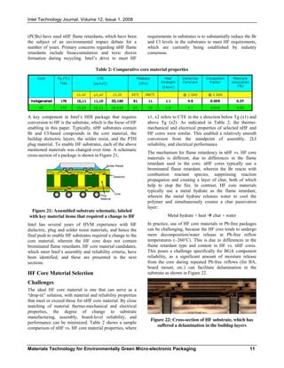
Table 1: LF failure concerns and recommended stress
testing
LF 2LI reliability challenges include delamination with
increased reflow temperature (35o
C higher than Sn/Pb),
lower mechanical margin in high strain rate shock testing
due to increased stiffness (1.5 times stiffer than SnPb
solder), creep performance difference compared to SnPb,
and Sn whiskers. The JEDEC specification for max reflow
spec of 260o
C was established as part of the solution, and
Intel components were qualified to meet the JEDEC
specification for peak reflow requirements. Use-condition-
based reliability performance was used for Pb-free alloy
selection. The LF mechanical margin was lower than that
for SnPb solder, but it passed intensive board-level shock
and vibe testing. The mechanical margin testing showed
lower mechanical performance compared to SnPb solder,
and the results are shown in Figure 3. The NCTF design
rule was implemented at corner joints for shock margins.
Figure 3: Mechanical margin assessment for LF solder
The failure mode during shock is manifested in cracking
along the solder joint (either on the package or board side)
as shown in Figure 4 [1].
Figure 4: SAC405 solder joint failure in shock
conditions
A detailed failure analysis reveals that the shock crack in
SAC is along the interface between the IMC and the
solder (package side) and through the IMC bulk (board
side). In either case, shock failure is characterized by a
lack of solder deformation and an absence of solder bulk
cracking. This is quite contrary to thermal fatigue failure
where the solder joint exhibits extensive inelastic
deformation that is often time-dependent.
This difference is partly due to the strain-rate sensitivity of
metallic materials. Metallic materials including solders
typically become stronger with increasing strain rates. In
other words, the flow stress increases with increasing
strain rates. The strain rate sensitivity is a strong function
of the homologous temperature (Thom), which is
considerably higher for solders, due to their low melting
temperatures.
As a result of the high strain rate sensitivity, the yield
strength of SAC solders increases rapidly with strain rate.
This increased yield strength suppresses any plastic
deformation and prevents the shock energy from
dissipating through the solder joint, thereby transferring
more stress to the interface which causes interfacial fails.
The yield strength of eutectic SnPb solder is relatively low
compared to the SAC405 solder alloy. This means SnPb
solders can dissipate more high strain rate energy through
deformation and hence can perform better in shock than a
SAC405 solder alloy. The higher yield strength of the
SAC405 solder alloy is derived primarily from the
precipitation hardening of the tin matrix by the Ag3Sn
precipitates/platelets. In addition to the increased bulk
strength of the SAC alloy, the higher reflow temperatures
can also cause an increased thickness in the IMC layers
and thereby degrade the shock performance of the
SAC405 solder alloy. However, the increased strength of
the SAC405 solder alloy is beneficial for thermal cycle
fatigue resistance as it reduces creep damage in each
LF Failures
Concern
Stress Test Comments
Solder fatigue Temp Cycle Electrical
open/solder crack
Overstressing Shock Test Electrical
open/solder crack
Overstressing Vib Test Electrical
open/solder crack
PCB trace,
via corrosion
Temp/Humid
85/85°C
Electrical open due to via, trace
corrosion
IMC growth,
Diffusion and Solder
creep
Bake Test Electrical open IMC growth,
diffusion, & shorts due to
solder creep
LF
LF
LF
4000ue
2700ue
1900ue
Corner
BoardStrain
000050Sn/Pb
00020100
100100100100100
00075100Sn/Pb
0040100100
0005050Sn/Pb
54321
CTFNonCTF
Crack (%)RowSolder
LF
LF
LF
4000ue
2700ue
1900ue
Corner
BoardStrain
000050Sn/Pb
00020100
100100100100100
00075100Sn/Pb
0040100100
0005050Sn/Pb
54321
CTFNonCTF
Crack (%)RowSolder
FEA Model
45](https://image.slidesharecdn.com/fbd9d1a0-b430-44e6-ab7f-1ac4ccb2c050-160416030809/85/Renavikar-IATTJ-2008-Green-Materials-for-Packaging-4-320.jpg)
![Intel Technology Journal, Volume 12, Issue 1, 2008
Materials Technology for Environmentally Green Micro-electronic Packaging 5
thermal cycle. Thus the transition from eutectic SnPb to
SAC405 solder alloy poses more challenges in high strain
rate shock applications, but provides more margin in
thermal cycle reliability.
The LF fatigue performance was about 20-30% higher
than SnPb for Flip Chip Ball Grid Array 9FCBGA
(FCBGAs). Temperature cycle results are compared with
the SnPb solder as shown in Figure 5. LF (SAC405)
showed improved fatigue performance in both 15-min.
and 30-min. dwell time testing.
Figure 5: LF temp cycle performance comparison with
Sn/Pb solder
LF creep performance concerns were addressed through
long dwell time testing. Long dwell time temperature
cycle testing (three cycles/day) were completed for
SAC405, and the results showed better LF performance
than SnPb solder as shown in Figure 6 [2].
Figure 6: LF Temp cycle performance in long dwell
time testing
The industry concern over long dwell time was
satisfactorily addressed based on these results, and the LF
reliability model correlation showed a similar type of fit
compared to that of Sn/Pb solder. The corrosion and
diffusion concerns were addressed through temperature
humidity testing (85/85 test) and bake test (125°C) for
1000 hrs. Bake testing did not show interface-related
failure mechanisms. The results are shown in Figure 7.
Figure 7: Bake test results for SAC405
with Im/Ag SF
The other LF reliability concern is the formation of tin
(Sn) whiskers. Sn whisker formation is not an issue for
Pb-free solders, but concerns the Sn surface finish on
components. The Sn whisker failure mechanism is an
electrical short caused due to the growth of the whisker.
An example of Sn whiskers is shown in Figure 8 [3].
Figure 8: Sn whiskers
The concern about Sn whiskers for Sn-coated components
is not related to LF issues, but it is the same as that for
Sn/Pb solder. JSTD 201 was established for Sn whisker
mitigation that includes the use of matte Sn and anneal at
higher temperatures for stress relief prior to SMT.
PCB surface finish quality characteristics have an impact
on reliability: micro void associated with Im/Ag PCB SF
quality characteristics negatively impacted the solder
fatigue margin (40-50% reduction in temperature cycle
performance). The impact of micro void on temperature
cycle performance is shown in Figure 9. The other
concern is a Kirkendall-type void in bake testing for OSP
Start
Percent
2500225020001750150012501000
99
95
90
80
70
60
50
40
30
20
10
5
1
Table of Statistics
118.168
7.10703 0.0937068 2.897
6.97849 0.0937068 1.110
Loc Scale AD*
7.54120 0.0937068 3.657
7.34854 0.0937068
Var
Pb-15min
Pb-30min
LF-15min
LF-30min
Probability Plot for Start
ArbitraryCensoring- MLEstimates
Lognormal
30 15mi
30 15
LFPb
%Failures
Cycles to Failure
Failure
Criteria: E-
test open
Larger
is
Better
Package Size: 37.5 mm sq
Die size: 11.7 X 8 mm, 4 Layer
Sn-Ag-Cu
405
TTII MMEE== 00
BBAAKKEE
TTEEMMPP== 11 00 00 oo
CC
TTII MMEE == 11 00 00 00 hhrrss
BBAAKKEE
TTEEMMPP== 11 22 55 oo
CC
TTII MMEE == 11 00 00 00 hhrrss
LF60
LF480
Pb60Pb480](https://image.slidesharecdn.com/fbd9d1a0-b430-44e6-ab7f-1ac4ccb2c050-160416030809/85/Renavikar-IATTJ-2008-Green-Materials-for-Packaging-5-320.jpg)
![Intel Technology Journal, Volume 12, Issue 1, 2008
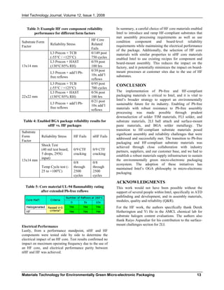
Materials Technology for Environmentally Green Micro-electronic Packaging 8
components as shown in Figure 14. The higher tin content
of the SAC solders causes more copper dissolution and
erosion, increasing barrel thinning. Use of newer Pb-free
alloys can alleviate this copper dissolution/erosion to a
large extent.
Figure 14: Copper erosion from minipot rework
Pb-free Initiative: Customer Manufacturing
Enabling Challenges
Given the significant challenges posed in the SMT
materials and processes to enable Pb-free transition, an
equivalent effort was needed to influence and enable the
ODM and OEM customer base to adopt the Pb-free
technologies and processes. The efforts undertaken by
Intel to influence the industry are outlined in this section.
Customer enabling for Pb-free board assembly consisted
of multiple steps over four years prior to the July 2006
RoHS date.
1. A customer-ready document, informally called the
Pb-free Manufacturing Advantage Service (MAS),
was prepared to capture technical learnings from the
Intel Lead Free Board Assembly Team (LFBAT). It
included tutorial information on all Pb-free board
assembly modules in a typical production line, and
also the Intel Reference Process for each module,
with detailed process parameters and process material
selections. It served as a starting point for customer
process development. The Pb-free MAS, containing a
substantial wealth of information, was developed in
order to meet customer’s requirements for more
detailed information.
2. Customer Manufacturing Enabling (CME), a new
group at the time, engaged major ODM and OEM
customers, delivered the Pb-free MAS in person
(primarily in APAC), and invited certain customers to
participate in further enabling activities.
3. One challenge with developing a board-level process
was the limited availability of Pb-free boards and
components. The CME team developed Pb-free test
boards, with Pb-free Bills of Material (BOMs),
representing designs from desktop, mobile, and server
market segments. Selected customers in each segment
were provided with board designs, or physical boards,
and BOMs, or physical parts, depending on their
preference.
4. Customers used the board kits (typically 75 boards) to
develop a board assembly process on their own. Both
Intel and customers then performed reliability tests on
samples of the boards and shared results.
5. After results from the development builds were
incorporated into customer processes, customers
completed another round of builds with Intel
representatives present, using additional Pb-free
board kits. These were called validation builds,
intended to confirm that the customer process could
consistently produce good boards over a larger
quantity (up to 200) in a manufacturing environment
(rather than a lab), without tweaking the process mid-
build. Again, Intel and customers separately
performed reliability testing, Failure Analysis (FA),
and Materials Analysis (MA) and again, shared
results.
6. Intel and customers held Manufacturing Readiness
Assessment meetings to review all results and
customer status regarding their own further
development work and builds of prototypes.
7. After the launch of Pb-free products, Intel monitored
customer manufacturing performance during launch
and ramp, providing assistance as needed.
By this process, Intel ensured a smooth launch and ramp
for the initial Pb-free platforms in each segment. In
addition, it helped drive industry convergence on a narrow
set of Pb-free materials that allowed Intel to produce Pb-
free components with only one ball alloy for all desktop,
mobile, and server products.
PB-FREE INITIATIVE: SOLDER
THERMAL INTERFACE MATERIALS
(STIM)
Intel’s foray into Pb-free materials in electronic packaging
began more than five years ago through the introduction
of STIM in the 90nm technology node products. The
relentless progress of Moore’s law, leading to a doubling
of transistor density in silicon chips every generation,
drove the need to develop thermal solutions to dissipate
additional heat generated in the silicon die. Consequently,
Intel’s packages have evolved from a bare die solution
catering to mobile market segments to Integrated Heat
Spreader (IHS) lidded products in desktop and server market
segments as shown in Figure 15 [4].](https://image.slidesharecdn.com/fbd9d1a0-b430-44e6-ab7f-1ac4ccb2c050-160416030809/85/Renavikar-IATTJ-2008-Green-Materials-for-Packaging-8-320.jpg)
![Intel Technology Journal, Volume 12, Issue 1, 2008
Materials Technology for Environmentally Green Micro-electronic Packaging 9
Figure 15: Evolution of Intel’s Package technology for
meeting thermal performance requirements
There are several technical and cost drivers to enable
lidded thermal architecture such as minimizing the impact
of local hot spots by improving heat spreading, increasing
the power-dissipation capability of the thermal solutions,
expanding the thermal envelopes of systems, developing
thermal solutions that meet business-related cost
constraints, as well as developing solutions that fit within
form-factor considerations of the chassis.
The primary role of the IHS is to spread the heat out
evenly from the die and to provide a better bondline
control of the interface material. This can be achieved by
increasing the area of the IHS and by using a high thermal
conductivity thermal interface material with low
interfacial resistances. In order to meet thermal dissipation
targets, Intel introduced polymer thermal interface
materials (PTIM) initially with 3-4 W/mo
K bulk thermal
conductivity and then successfully transitioned to Pb-free
solder-based thermal interface material to meet the ever
increasing demand for thermal cooling capability as
shown in Figure 16 [5].
Figure 16: Improvement in thermal cooling capability
with TIM materials (Polymer vs. Solder)
The introduction of Pb-free solder-based TIM materials
posed significant integration challenges. The STIM
needed to relieve the mechanical stress caused by CTE
mismatch of the integrated heat spreader lid and the
silicon die and to minimize stress transfer to the silicon
die during thermal cycling [6]. The thermal conductivity
and the mechanical compliance requirements resulted in
the development and qualification of low melting
temperatures (157o
C Tm), low mechanical yield strength
(4-6 MPa), and relatively high thermal conductivity (~87
W/mo
K) pure Indium (In) metal for STIM applications. In
order to use In for STIM applications, appropriate flux
vehicles had to be developed to a) effectively reduce the
thermodynamically stable native Indium oxide on In
performs; b) to control solder joint voiding post joint
formation; c) to control interfacial reactions with surface
finishes on the IHS lid and the back side metallization
(BSM) on the silicon die; and d) to deal with reliability
issues faced in small and large die products, such as
thermal fatigue cracking of the Indium during thermal
cycling. The assembly process, including the reflow of the
Indium STIM to form uniform intermetallic compounds
(IMCs) post assembly, is a key challenge. A schematic of
the STIM microstructural development as a function of
packaging assembly steps is shown in Figure 17. The
Indium oxide on the surface of the Indium needs to be
effectively reduced in order to form uniform and defect-
free intermetallic layers at both the die/Indium and the
IHS lid plating (Ni/Au) and the In. Indium oxide is an
extremely tenacious and thermodynamically stable oxide
as shown in Figure 18 [7]. The presence of voiding in the
joint can potentially lead to an increase in local thermal
resistance and consequently lead to the degradation of the
thermal performance of the joint. Additionally, excessive
spallation of the binary Au-In IMCs as well as the
formation of excessive Kirkendall voiding due to
relatively different diffusion coefficients of In-Au and Ni
can result in an increase in the thermal resistance of the
joint.
Figure 17: Use of Indium metal as STIM and
interactions with surface finish on IHS and BSM pre
and post assembly](https://image.slidesharecdn.com/fbd9d1a0-b430-44e6-ab7f-1ac4ccb2c050-160416030809/85/Renavikar-IATTJ-2008-Green-Materials-for-Packaging-9-320.jpg)
![Intel Technology Journal, Volume 12, Issue 1, 2008
Materials Technology for Environmentally Green Micro-electronic Packaging 10
Figure 18: Thermodynamic stability of Indium Oxide
as a function of temperature
In reliability testing as in thermal cycling, tensile and
shear stresses are imposed on the STIM joint due to the
mechanical coupling of the die to the IHS lid and the
package as shown in Figure 19.
Figure 19: Warpage induced stresses on STIM joint at
low temperature and high temp thermal cycling
(Numbers in figure indicate different locations along
package)
Typical failure modes encountered in STIM joints relate
to thermal fatigue cracking of Indium close to the
IHS/Indium interface which is manifested in the form of a
white signature in CSAM imaging as shown in Figure 20
[6].
Figure 20: White CSAM image showing delamination
at the Indium/IHS interface and corresponding cross-
section SEM image showing cracking post reliability
testing
The reliability performance of the STIM joints has been
found to be modulated by the relative thickness and
morphology of the binary and ternary IMCs as influenced
by the fluxing ability of the flux used and the reflow
profile used, as well as several mechanical design
attributes of the IHS dimensions/die size, package
stiffness, and preform dimensions. In addition to the
technical challenges faced in enabling Indium, a
significant effort was made to establish a strong supply
chain for IHS lid manufacturing and plating, sealant
materials technology for attaching the IHS lid to the
substrate, as well as the development of appropriate back
side metallization on the die to enable interfacial reactions
with STIM to ensure robust joint formation.
In summary, Intel’s transition to Pb-free packaging
materials technology was attained through a judicious
choice of materials across all functional areas such as FLI,
2LI, and STIM. The Pb-free materials solutions met all
the integration assembly and surface-mount challenges as
well as component and board-level reliability
requirements. Intel worked closely with industry partners
including suppliers and the ODM and OEM customer base
to achieve a smooth launch and ramp of the Pb-free
packaging materials technologies.
We now discuss Intel’s stewardship in enabling HF-
compliant packaging materials initiatives specifically the
enabling of HF substrates technology.
HALOGEN-FREE PACKAGING
MATERIALS INITIATIVE
As part of Intel’s broad strategy to support an
environmentally sustainable future, Intel is introducing
environmentally conscious HF and Pb-free packaging at
the 45nm CPU and 65nm chipset technology nodes. HF
packaging materials introduced by Intel include several
materials such as molding compounds, underfill materials,
and substrates. The scope of this section of this paper is
limited to HF-compliant substrate technology.
Historically, components and printed circuit boards](https://image.slidesharecdn.com/fbd9d1a0-b430-44e6-ab7f-1ac4ccb2c050-160416030809/85/Renavikar-IATTJ-2008-Green-Materials-for-Packaging-10-320.jpg)
![Intel Technology Journal, Volume 12, Issue 1, 2008
Materials Technology for Environmentally Green Micro-electronic Packaging 12
To address this concern, a reflow accelerated test best
known method (BKM) was implemented and used in the
HF core material downselection process. The reflow
accelerated test BKM incorporated JEDEC Pb-free Level
3 preconditioning (L3 precon) [8] with stepwise,
additional Pb-free reflows (@ 260°C), to check for the
delamination margin in the HF product substrates. Up to
15x additional reflows (beyond L3 precon) were run to
test the delamination margin. Through careful material
selection and screening, robust core materials, that met
Intel’s reliability requirements, were identified.
HF Core Material Results
HF core material selection required us to focus on
substrate manufacturing, component and board-mount
assembly, reliability testing, and performance. The results
from these evaluations are presented in the following
sections.
Substrate Manufacturing
From the substrate manufacturing perspective, the key
challenges were selection of robust core materials,
followed by mechanical drilling and flatness assessments
of those materials. To select the most robust core
materials, substrate suppliers were engaged and enabled
with the reflow accelerated test BKM. Thorough
evaluations were performed on various short and full loop
test vehicles (TVs) with different designs, to understand
the impact of core material and design on delamination
reliability. Based on the number of reflows before the
occurrence of delamination, the core materials with the
most robust heat resistance were selected for further
evaluation. These core materials were confirmed to be HF
at Intel through ion chromatography testing, with the Br
and Cl contents measuring <4 ppm. Core material
drillability, as well as drill bit life parity between nHF and
HF core, was established across the substrate supply base
through drilling evaluations on the downselected
materials. The parity in drill bit life ensures that there is
no increase in drilling costs when an HF core is used. By
measuring substrate flatness on incoming substrates, it was
shown that HF core and nHF core units were equivalent
across the substrate supply base.
Intel Assembly
The above trend carried forth through Intel assembly,
wherein HF substrate flatness was the key assembly
concern. Figure 23 shows comparative HF vs. nHF BGA
ball coplanarity data for a 13x14mm TV. The data
confirm that HF and nHF cores have similar flatness
performance.
Figure 23: Comparison of HF to nHF package
coplanarity for 13x14 mm TV
Board mount of nHF vs. HF components was also studied,
with results indicating similar board-mount yields for both
nHF and HF units.
HF Substrates Component Reliability
Reliability testing at the component level involved use of
Intel’s new Pb-free L3 preconditioning plus up to 15x
additional reflows at 260°C, to check for delamination
margins. A number of HF core materials were dropped
from consideration because of delamination margins. The
selected HF core materials were robust during reliability
testing, and for the given form factors/designs in Table 3,
passed more than 10x additional reflows beyond L3
preconditioning before any delamination was observed.
Reliability results were similar for substrates across Intel’s
supply base, indicating sufficient reliability transparency.
HF Substrates Enabled Reliability
Enabled reliability testing (component mounted on the
board) also showed performance parity between nHF and
HF core TVs as shown in Table 4. In shock testing (a.k.a.
dynamic bend testing), neither nHF nor HF substrates
showed cracks in any critical to function (CTF) BGA
solder joints.
Flammability Rating
Due to concern about flame retardant decomposition
during multiple Pb-free reflows for BGA products, and the
potential implications of this for flammability rating, a
check of the UL-94 flammability rating before and after
extended Pb-free reflows was done. Table 5 shows the
results, which indicate that both nHF and HF core
materials were able to maintain a V-0 flammability rating
after 10x Pb-free reflows.
Pkg.Coplanarity(mils)
1
2
3
4
5
6
7
HF nHF
HF/ nHF
Variability Chart for Coplanarity (mils)](https://image.slidesharecdn.com/fbd9d1a0-b430-44e6-ab7f-1ac4ccb2c050-160416030809/85/Renavikar-IATTJ-2008-Green-Materials-for-Packaging-12-320.jpg)
![Intel Technology Journal, Volume 12, Issue 1, 2008
Materials Technology for Environmentally Green Micro-electronic Packaging 14
REFERENCES
[1] Daewoong Suh et al., “Effects of Ag content on
fracture resistance of Sn-Ag-Cu lead-free solders
under high strain rate conditions,” Materials Science
and Engineering A, 46-461, 2007, pps. 595–603.
[2] Vasu Vasudevan et al., “Slow Cycle Fatigue Creep
Performance of Pb-free (LF) Solders,” ECTC, 2007.
[3] Irina Boguslavsky et al., “Recrystallization Principles
Applied to Whisker Growth in Tin”, APEX
Conference, March 31, 2003, Anaheim, CA,
pps. 1–14.
[4] R. Mahajan et al., “Advances and Challenges in Flip-
Chip Packaging,” IEEE 2006 Custom Integrated
Circuits Conference, (CICC), 2006.
[5] V. Wakharkar et al., “Microelectronic Packaging
Materials Development & Integration Challenges for
Lead Free,” TMS Conference, 2006.
[6] Carl Deppisch et al., “Material Optimization and
Reliability Characterization of Indium Solder Thermal
Interface Materials for 1262 Package technology,”
IATTJ Journal, Vol. 5, 2002, pps. 227–240.
[7] Smithell’s Metals Reference Book, E. A. Brandes and
G.B. Brook (editors), Seventh edition, 1992,
Butterworth Heineman, London, England.
[8] JEDEC J-STD-020.
AUTHORS’ BIOGRAPHIES
Mukul Renavikar is a Senior Packaging Engineer in the
ATTD-Materials group. He has been with Intel for over
four years and leads the Metallurgy/Materials Core
Competency group in Assembly and Test Technology
Development (ATTD). Mukul received his Bachelor’s
degree in Metallurgy from the College of Engineering,
Pune, and M.S. and PhD degrees in Materials Science
from the University of Pittsburgh, PA. His e-mail is
mukul.p.renavikar at intel.com.
Neha Patel is a Senior Materials Engineer in the ATTD
group. She has been with Intel for three years and has
worked extensively in the area of first-level interconnect
polymer materials and thermal interface materials. She
obtained her bachelors degree in Physics from St. Xaviers
college, Bombay and M.S. and PhD degrees in Physics
from Case Western Reserve University Cleveland, OH.
Her e-mail is neha.m.patel at intel.com.
Ashay Dani obtained his B.S. degree in Chemical
Engineering from UDCT, Bombay, India and a PhD
degree in Chemical Engineering from Clemson
University. Ashay joined Intel in 2000 and has managed
several packaging materials and suppliers’ technology
development, certification and ramp. His e-mail is
ashay.a.dani at intel.com..
Vijay Wakharkar is a Principal Engineer in ATTD and
has worked at Intel for 17 years. Vijay got his Bachelors
degree from the College of Engineering, Poona in 1982
and his PhD degree in Materials Science and Engineering
in 1988. Prior to joining Intel, he spent two years as a Post
Doctoral Fellow at IBM Almaden Research Center in the
Polymer Materials Division. Currently he is responsible
for managing the development and path-finding of
materials technologies that end up in ATTD’s packaging
solutions. Vijay was one of the founding editors of the
Intel Assembly Technology and Test Journal (IATTJ) and
also serves on Intel’s Thermo-mechanical Patent
Committee. His e-mail is vijay.s.wakharkar at intel.com.
Omar Bchir is a Senior Packaging Engineer in the
substrates pathfinding group with Intel-ATTD, and he has
been with Intel for over three years. His focus areas have
been metallization, integration, and HF enabling. Omar
obtained his Bachelor’s degree in Chemical Engineering
from the Georgia Institute of Technology in 1997 and his
PhD degree in Chemical Engineering from the University
of Florida in 2004. His e-mail is omar.j.bchir at intel.com..
Amruthavalli Pallavi Alur is a Senior Packaging
Engineer in the substrates pathfinding group with Intel-
ATTD, and she has been with Intel for two years. Her
focus area includes Mechanics of Materials and HF
enabling. Pallavi obtained her Bachelor’s degree in
Metallurgy and Materials Sciences from the Institute of
Technology (India) in 2000 and her PhD degree in
Materials Science and Engineering from Brown
University in 2005. Her e-mail is amruthavalli.p.alur at
intel.com.
Charan Gurumurthy manages ATTD’s substrate
pathfinding group and has been with Intel for over five
years. Before joining Intel, he worked at IBMs
Microelectronics Division in Endicott, NY. Charan
obtained his Bachelor’s degree in Mechanical Engineering
from the Indian Institute of Technology in 1994 and his
PhD in Materials Science and Engineering from Cornell
University in 2000. He has 30 + patents awarded/filed and
10+ journal publications. He currently serves as
“Associate Editor” of IEEE Transactions on Advanced
Packaging and is a senior member of IEEE. His e-mail is
charan.k.gurumurthy at intel.com.
Roger Stage has a PhD degree in Mechanical
Engineering from Arizona State University. Dr. Stage
manages package quality and reliability engineering in
Intel’s Assembly Technology Development Quality &
Reliability organization in Chandler, Arizona. His e-mail
is roger.w.stage at intel.com.](https://image.slidesharecdn.com/fbd9d1a0-b430-44e6-ab7f-1ac4ccb2c050-160416030809/85/Renavikar-IATTJ-2008-Green-Materials-for-Packaging-14-320.jpg)