
Recommended
More Related Content
What's hot
What's hot (20)
Similar to Associative memory
More from NancyBeaulah_R
Recently uploaded
Recently uploaded (20)
Associative memory
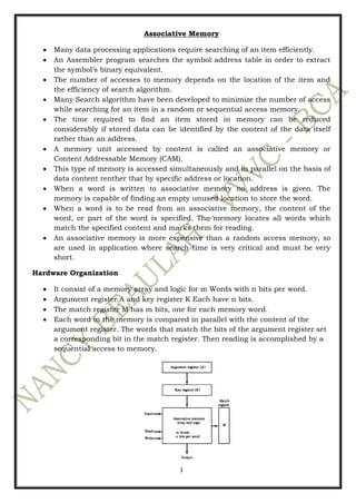
- 1. 1 Associative Memory Many data processing applications require searching of an item efficiently. An Assembler program searches the symbol address table in order to extract the symbol’s binary equivalent. The number of accesses to memory depends on the location of the item and the efficiency of search algorithm. Many Search algorithm have been developed to minimize the number of access while searching for an item in a random or sequential access memory. The time required to find an item stored in memory can be reduced considerably if stored data can be identified by the content of the data itself rather than an address. A memory unit accessed by content is called an associative memory or Content Addressable Memory (CAM). This type of memory is accessed simultaneously and in parallel on the basis of data content renther that by specific address or location. When a word is written to associative memory no address is given. The memory is capable of finding an empty unused location to store the word. When a word is to be read from an associative memory, the content of the word, or part of the word is specified. The memory locates all words which match the specified content and marks them for reading. An associative memory is more expensive than a random access memory, so are used in application where search time is very critical and must be very short. Hardware Organization It consist of a memory array and logic for m Words with n bits per word. Argument register A and key register K Each have n bits. The match register M has m bits, one for each memory word. Each word in the memory is compared in parallel with the content of the argument register. The words that match the bits of the argument register set a corresponding bit in the match register. Then reading is accomplished by a sequential access to memory.
- 2. 2 Key register It provides a mask for choosing a particular field or key in the argument word. The entire argument is compared with each memory word if the key register contains all 1’s. Otherwise, only those bits in the argument that have 1’s in their corresponding position of the key register are compared. Example Relationship between the memory array and external registers Cell Cij is the cell for bit j in word i. A bit Aj in the argument register is compared with all bits in column j of the array provided that kj =1. This is done for all comumns j=1,2,…,n. If match occurs between all the unmasked bits of the argument and the bits in word I, then set Mi to 1. Otherwise set Mi to 0.
- 3. 3 One cell of associative memory It consist of a flip-flop storage element Fij and circuit for reading, writing , and matching the cell. Match Logic Word i is equal to the argument in A if Aj=Fij for j=1,2,..,n. Two bits are equal if they are both 1 or both 0. The equality of two bits can be expressed logically by Boolean function. xj= AjFij + Aj’Fij’ where xj = 1 if the pair of bits in position j are equal; otherwise, xj=0. For a word i to be equal to the argument in A we must have all xj variables equal to 1. This is the condition for setting the corresponding match bit Mi to 1. Boolean function for this condition is Mi =x1x2… xn If kj=0, the corresponding bits of Aj and Fij need no comparison. Only when Kj=1 must they be compared. This requirement is achieved by ORing each term with Kj’, thus { The match logic for word i in an associative memory can now be expressed by the following Boolean function. Mi = (x1 + K1’) (x2 + K2’) (x3 + K3’) … (xn + Kn’) If we substitute the original definition of xj. Mi = ∏ (AjFij + Aj’Fij’+ Kj’) where ∏ is a product symbol designating the AND operation of all n terms.
- 4. 4 Each cell requires 2 AND gets and one OR gate. The inverters for Aj and Kj are needed once for each column and are used for all bits in the column. The output to all OR gates in the cells of the same word go to the input of the common AND get to Generate the match signal for Mi. Read Operation if more than one word in memory matches, then read in sequence by applying read signal to each word line with Mi =1. If only one word may match, connect output Mi directly to the read line in the same word position. Write Operation Writing in an associative memory can take different forms. If entire memory is loaded with new information, then writing can be done by addressing each location in sequence. If unwanted words have to be deleted and new words inserted one at a time using tag register. A word is deleted for memory be clearing its tag bit to 0. After the new word is stored in memory it is made active by setting its tag bit to 1.