
Recommended
More Related Content
What's hot
What's hot (20)
Viewers also liked
Viewers also liked (14)
Similar to WSU EECS REU poster
Similar to WSU EECS REU poster (20)
WSU EECS REU poster
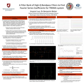
- 1. A Filter Bank of High-‐Q Bandpass Filters to Find Fourier Series Coefficients for TRDMA system Jinyanzi Luo, Dr.Benjamin Belzer School of Electrical Engineering and Computer Science Washington State University, Pullman, WA 99164 Motivation ● Previously proposed TRDMA systems utilized digital sampling, which is not practical for WiNoCs due to extremely short- duration on-chip impulse response, so analog TRDMA system is need to be designed. ● TRDMA offers a power and area efficient method by creating spatial channels between each Tx/Rx pair in WiNoC. Time Reversal Division Multiple Access (TRDMA) ● A wirelessly transmitted signal will take multiple paths to a receiving antenna, a phenomenon known as the multipath effect. TRDMA takes advantage of this multipath effect via channel reciprocity to spatially and temporally focus all of a signal’s energy on a desired receiver. Utilizing TRDMA for wireless network-on-chip (WiNoC) application can: 1. Reduce the power needed to transmit information between processors that are far apart. 2. Enable multiple omni-directional antennas to transmit information to multiple receivers simultaneously using spatial multiplexing, while avoiding temporal inter- symbol interference(ISI). ● An impulse at a receiving node using TRDMA can be achieved by sending a time-reversed impulse response from a transmitting antenna. In order to accomplish this: 1. The impulse response from Rx to Tx must first be obtained by Tx during a recording phase. 2. The impulse response must then be time-reversed and sent by the Tx during the transmitting phase. ● At WiNoC data rates (ten of Gb/s) it is currently not possible to digitally record the impulse response, so the impulse response must be learned via an analog circuit ● On-chip antennas that employ Wireless Network-on-chip (WiNoc) systems allow wireless communication between cores across long distances. Introduction I would like to specially thank : ● Dr.Benjamin Belzer, Joe Balyon, and Jorge Pires for their help on this project. ● Noel Wang and Kevin Johnson for providing a foundaWon for this research. ● WSU EECS faculty and staff for making this research possible. This work was supported by the NaWonal Science FoundaWon’s REU program under grant number CNS 1359461 Acknowledgement Results Method ● A commercial circuit simulation software package called Cadence is used to construct the filter bank. ● The input signal of the bank is the impulse response from a Finite Difference Time Domain simulation of on-chip wireless transmission. Conclusion Future Work Fourier Series ● Fourier discovered that a periodic function can be represented by an infinite sum of sine or cosine functions that are harmonically related. ● Signals can be approximated by Fourier Series via the following the expression: ● A time-reversed version of the waveform is computed by inverting the signs in front of the bn coefficients. ● Self-calibration circuit for the coefficient sampling times is needed. ● Summing all the coefficients to generate the time-reversed waveform of the incoming impulse. ● These antennas suffer from high power dissipation and timing delays due to their token-passing wireless access control protocols. ● The Fourier Series (FS) coefficients are needed to recreate or to store the impulse waveform that is sent from Rx to Tx during the recording phase. ● To demonstrate the feasibility of analog TRDMA with FS approximations, a filter bank of high-Q bandpass filters are designed in order to calculate the FS coefficients Introduction Cont. Fig 3. Filter Bank Circuitry: contains integrator, voltage followers/buffer, voltage gains, switches, capacitors, resistors and bandpass filters. Fig 2. Two GHz High-Q bandpass filter circuitry, which is derived from inductor-less Antoniou circuit Fig 1. Block diagram for computing the first 10 FS coefficients with bandpass filters Fig 3. a0 waveforms: switch opens at T = 2𝝅/⍵0, where ⍵0 is fundamental frequency we set it to 1GHz, so T=1ns Fig 5. A square wave going through the second filter for finding the second pair of FS coefficients Fig 4. Found delays through the filters, which did not happen in LTSpice simulation ● Switches in the bank are calibrated to open at correct peak and zero-crossing time for cosine and sine input waveforms. ● The coefficients became less accurate after the 7th filter, no solution has found yet to what caused this phenomenon. ● At the high frequencies simulated by Cadence, the delays through the circuits must be taken into account when sampling the an and bn coefficients. Fig 6. Four methods of computing Fourier Series Coefficients are compared with the ideal coefficients given in mathematical formulas.