SlideShare a Scribd company logo
1 of 7
Download to read offline
Jeff Webb
ELEC 3700
LTSpice Op Amp Design Project
8/1/2016
The operational amplifier is a fundamental building block of analog circuit design. The
primary goal of this project is to use LTSpice to design and simulate an operational amplifier
meeting a certain set of specifications. The input is a 5 mV amplitude source with a frequency of
20 kHz, a 2 kΩ source resistance, and a DC value with a range of -1 V to +1 V. Supply voltage is
provided by two 9 V batteries. The required output is a 5 V amplitude sinusoid across a 100 Ω
load resistance with an average value of 0 V and minimal distortion. The design exhibited in this
project utilizes 2N3904 npn and 2N3906 pnp BJT’s, as well as standard resistor values that are
present within the Jaeger appendix for 1% values. The following screenshot shows the topology
of my op amp design. This design is very close to meeting the desired specifications per the
project guidelines.
Figure 1: Multistage op amp
The first functional block that will be discussed is the differential input stage given in the
figure below.
Figure 2: Differential input stage with current mirror load
The differential input stage forms the backbone of the op amp circuit. This stage is a
bipolar differential amplifier with two npn transistors and an active current mirror load formed
from a pnp current mirror as shown. The current mirror is used to enhance the voltage gain
capability while helping to maintain the operating point balance that is necessary for good
common-mode rejection.
The current mirror circuit given below is formed by two npn transistors and a Rref
resistor.
Figure 3: Current mirror circuit
Current mirror biasing is extremely important in this design. A reference current is
established by using resistor Rref that provides operating bias to the current mirror. A large value
of resistance is required to achieve a small operating current that is independent of the supply
voltage.
Lastly, the last two stages of the op amp shown below are discussed.
Figure 4: pnp common-emitter stage and npn output stage
An op amp usually requires higher voltage gain than is available from a single differential
amplifier stage. To achieve a higher gain, a pnp common-emitter amplifier Q3 is added by
connecting it to the output of the differential amplifier. The resistor R3 is added at the collector
of the pnp to help obtain a better output signal centered at 0 V. The output stage Q4 is added to
maintain unity voltage gain and provide low output resistance. The input resistance is set by the
input differential pair, and the output resistance is determined by the resistance looking into the
emitter of Q4.
I measured the differential and common mode gain of my op amp using LTSpice. For the
differential mode gain, I wired a voltage source to the two inputs of the op amp and specified a
voltage of 1 V AC. Next, I ran an AC analysis simulation to obtain the Bode plot shown below.
Figure 5: Circuit schematic and Bode plot corresponding to differential mode response
In order to measure the common mode gain, I shorted the two input terminals of my op
amp and wired it to the positive terminal of a 1 V AC voltage source. Next, I ran an AC analysis
simulation to obtain the common mode response shown below.
Figure 6: Circuit schematic and Bode plot corresponding to common mode response
I also measured total quiescent power dissipation and DC operating points for -1, 0, and
+1 V in LTSpice. These values are easily found by running the op amp, hovering the cursor over
the output and reading the values at the bottom of the screen.
Given below is a table summarizing all of the aforementioned and required quantities for
my op amp:
DC input Differential
Mode Gain
Common
Mode Gain
CMRR Dissipated
Power
DC Output
-1 V 2511 v/v .05 v/v 94 dB 982.4 mW 911.4 mV
0 V 2511 v/v .05 v/v 94 dB 993.3 mW 966.5 mV
+1 V 2511 v/v .05 v/v 94 dB 982.4 mW 911.4 mV
The following screenshots show plots of the output of my op amp at DC values of 0, -1,
and +1 V.
Figure 7: Output at 0 V DC
Figure 8: Output at -1 V DC
Figure 9: Output at +1 V DC
Figure 10: Average value of output waveform
The results in each plot give an output waveform with an amplitude of about 5.1 V with
minimum distortion and an average value of 480.89 mV. This is as close as I could get to the
required output amplitude of 5 V with 0 V average value. I think this is a good op amp and I am
pleased with this design. It provides good overall characteristics: desired gain, CMRR and good
frequency response. Overall, this project has taught me a great deal about the behavior and
characteristics of multistage amplifiers. I am confident that the knowledge and experience I have
gained from this project will stimulate my future endeavors next semester in radio lab.

More Related Content

What's hot

OPERATIONAL AMPLIFIERS
OPERATIONAL AMPLIFIERSOPERATIONAL AMPLIFIERS
OPERATIONAL AMPLIFIERSTamilarasan N
 
operational amplifiers
operational amplifiersoperational amplifiers
operational amplifiersPatel Jay
 
OPERATIONAL AMPLIFIERS, DIFFERENTIAL, NON-INVERTING AND INSTRUMENTATIONAL AMP...
OPERATIONAL AMPLIFIERS, DIFFERENTIAL, NON-INVERTING AND INSTRUMENTATIONAL AMP...OPERATIONAL AMPLIFIERS, DIFFERENTIAL, NON-INVERTING AND INSTRUMENTATIONAL AMP...
OPERATIONAL AMPLIFIERS, DIFFERENTIAL, NON-INVERTING AND INSTRUMENTATIONAL AMP...Kramikauniyal
 
A presentation of design,math and explanation of non inverting
A presentation of design,math and explanation of non invertingA presentation of design,math and explanation of non inverting
A presentation of design,math and explanation of non invertingHimel Himo
 
OP amp parameters
OP amp parametersOP amp parameters
OP amp parametersOmkar Rane
 
Operational Amplifiers I
Operational Amplifiers IOperational Amplifiers I
Operational Amplifiers Iali_craigslist
 
E ② chapter one - feedback amplifier
E ②   chapter one - feedback amplifierE ②   chapter one - feedback amplifier
E ② chapter one - feedback amplifierhaylat andu
 
Operational Amplifiers
Operational AmplifiersOperational Amplifiers
Operational Amplifierstaruntiru
 
Op-Amp Fundamental
Op-Amp FundamentalOp-Amp Fundamental
Op-Amp FundamentalGaensan
 
ANALYSIS ON CLASS-A VOLTAGE FOLLOWER
ANALYSIS ON CLASS-A VOLTAGE FOLLOWERANALYSIS ON CLASS-A VOLTAGE FOLLOWER
ANALYSIS ON CLASS-A VOLTAGE FOLLOWERJournal For Research
 
Unit-II Applications of Operational Amplifier
Unit-II Applications of Operational AmplifierUnit-II Applications of Operational Amplifier
Unit-II Applications of Operational AmplifierDr.Raja R
 
Slew rate, Open and closed loop configurations
Slew rate, Open and closed loop configurationsSlew rate, Open and closed loop configurations
Slew rate, Open and closed loop configurationsGOWRISHANKAR RAJU
 
Op amp comparator
Op amp comparatorOp amp comparator
Op amp comparatorAhmadoof
 
CE CB (cascade) amplifier
CE CB (cascade) amplifierCE CB (cascade) amplifier
CE CB (cascade) amplifierRakesh Makhija
 

What's hot (20)

OPERATIONAL AMPLIFIERS
OPERATIONAL AMPLIFIERSOPERATIONAL AMPLIFIERS
OPERATIONAL AMPLIFIERS
 
operational amplifiers
operational amplifiersoperational amplifiers
operational amplifiers
 
OPERATIONAL AMPLIFIERS, DIFFERENTIAL, NON-INVERTING AND INSTRUMENTATIONAL AMP...
OPERATIONAL AMPLIFIERS, DIFFERENTIAL, NON-INVERTING AND INSTRUMENTATIONAL AMP...OPERATIONAL AMPLIFIERS, DIFFERENTIAL, NON-INVERTING AND INSTRUMENTATIONAL AMP...
OPERATIONAL AMPLIFIERS, DIFFERENTIAL, NON-INVERTING AND INSTRUMENTATIONAL AMP...
 
A presentation of design,math and explanation of non inverting
A presentation of design,math and explanation of non invertingA presentation of design,math and explanation of non inverting
A presentation of design,math and explanation of non inverting
 
OP amp parameters
OP amp parametersOP amp parameters
OP amp parameters
 
Summing Amplifer
Summing AmpliferSumming Amplifer
Summing Amplifer
 
Seminar final
Seminar finalSeminar final
Seminar final
 
Tarun
TarunTarun
Tarun
 
Operational Amplifiers I
Operational Amplifiers IOperational Amplifiers I
Operational Amplifiers I
 
E ② chapter one - feedback amplifier
E ②   chapter one - feedback amplifierE ②   chapter one - feedback amplifier
E ② chapter one - feedback amplifier
 
Operational Amplifiers
Operational AmplifiersOperational Amplifiers
Operational Amplifiers
 
Op-Amp Fundamental
Op-Amp FundamentalOp-Amp Fundamental
Op-Amp Fundamental
 
feedback amplifier
 feedback amplifier feedback amplifier
feedback amplifier
 
Operational amplifier
Operational amplifierOperational amplifier
Operational amplifier
 
ANALYSIS ON CLASS-A VOLTAGE FOLLOWER
ANALYSIS ON CLASS-A VOLTAGE FOLLOWERANALYSIS ON CLASS-A VOLTAGE FOLLOWER
ANALYSIS ON CLASS-A VOLTAGE FOLLOWER
 
Feedback in amplifier
Feedback in amplifierFeedback in amplifier
Feedback in amplifier
 
Unit-II Applications of Operational Amplifier
Unit-II Applications of Operational AmplifierUnit-II Applications of Operational Amplifier
Unit-II Applications of Operational Amplifier
 
Slew rate, Open and closed loop configurations
Slew rate, Open and closed loop configurationsSlew rate, Open and closed loop configurations
Slew rate, Open and closed loop configurations
 
Op amp comparator
Op amp comparatorOp amp comparator
Op amp comparator
 
CE CB (cascade) amplifier
CE CB (cascade) amplifierCE CB (cascade) amplifier
CE CB (cascade) amplifier
 

Similar to Op ampdesignfinalproject

Unit-I Characteristics of opamp
Unit-I Characteristics of opampUnit-I Characteristics of opamp
Unit-I Characteristics of opampDr.Raja R
 
Switching Voltage Regulator
Switching Voltage RegulatorSwitching Voltage Regulator
Switching Voltage Regulatoribercovich
 
Chapter 7: Operational Amplifier (Op-Amp)
Chapter 7: Operational Amplifier (Op-Amp)Chapter 7: Operational Amplifier (Op-Amp)
Chapter 7: Operational Amplifier (Op-Amp)JeremyLauKarHei
 
Electronic circuit design lab manual
Electronic circuit design lab manualElectronic circuit design lab manual
Electronic circuit design lab manualawais ahmad
 
Circuit theory 1 finals
Circuit theory 1 finalsCircuit theory 1 finals
Circuit theory 1 finalsjerbor
 
Circuit theory 1 finals
Circuit theory 1 finalsCircuit theory 1 finals
Circuit theory 1 finalsjerbor
 
Chapter 05. ppt operational amplifier
Chapter 05.    ppt operational amplifierChapter 05.    ppt operational amplifier
Chapter 05. ppt operational amplifiercbcbgdfgsdf
 
EC3451 LINEAR INTEGRATED CIRCUITS UNIT 1 .pdf
EC3451 LINEAR INTEGRATED CIRCUITS UNIT 1 .pdfEC3451 LINEAR INTEGRATED CIRCUITS UNIT 1 .pdf
EC3451 LINEAR INTEGRATED CIRCUITS UNIT 1 .pdfVanithaR25
 
Bipolar junction transistor characterstics biassing and amplification, lab 9
Bipolar junction transistor characterstics biassing and amplification, lab 9Bipolar junction transistor characterstics biassing and amplification, lab 9
Bipolar junction transistor characterstics biassing and amplification, lab 9kehali Haileselassie
 
Operational amplifier UA741
Operational amplifier UA741Operational amplifier UA741
Operational amplifier UA741unni krishnan
 
ECE 312 Current Feedback Operational Amplifier (final project)
ECE 312 Current Feedback Operational Amplifier (final project)ECE 312 Current Feedback Operational Amplifier (final project)
ECE 312 Current Feedback Operational Amplifier (final project)Jonathan Lepp
 
4_INFRARED REMOTE USED FOR 8
4_INFRARED REMOTE USED FOR 84_INFRARED REMOTE USED FOR 8
4_INFRARED REMOTE USED FOR 8SURAJ MAHAPATRA
 
Experiment no 2 setb118
Experiment no 2    setb118Experiment no 2    setb118
Experiment no 2 setb118Omkar Rane
 
SIGNAL SPECTRA EXPERIMENT 1 - FINALS (for ABDON)
SIGNAL SPECTRA EXPERIMENT 1 - FINALS (for ABDON)SIGNAL SPECTRA EXPERIMENT 1 - FINALS (for ABDON)
SIGNAL SPECTRA EXPERIMENT 1 - FINALS (for ABDON)Sarah Krystelle
 
Integrated Circuit Applications
Integrated Circuit ApplicationsIntegrated Circuit Applications
Integrated Circuit ApplicationsUMAKANTH22
 

Similar to Op ampdesignfinalproject (20)

Unit-I Characteristics of opamp
Unit-I Characteristics of opampUnit-I Characteristics of opamp
Unit-I Characteristics of opamp
 
Switching Voltage Regulator
Switching Voltage RegulatorSwitching Voltage Regulator
Switching Voltage Regulator
 
Lab1
Lab1Lab1
Lab1
 
Chapter 7: Operational Amplifier (Op-Amp)
Chapter 7: Operational Amplifier (Op-Amp)Chapter 7: Operational Amplifier (Op-Amp)
Chapter 7: Operational Amplifier (Op-Amp)
 
Electronic circuit design lab manual
Electronic circuit design lab manualElectronic circuit design lab manual
Electronic circuit design lab manual
 
Circuit theory 1 finals
Circuit theory 1 finalsCircuit theory 1 finals
Circuit theory 1 finals
 
Circuit theory 1 finals
Circuit theory 1 finalsCircuit theory 1 finals
Circuit theory 1 finals
 
Chapter 05. ppt operational amplifier
Chapter 05.    ppt operational amplifierChapter 05.    ppt operational amplifier
Chapter 05. ppt operational amplifier
 
EC3451 LINEAR INTEGRATED CIRCUITS UNIT 1 .pdf
EC3451 LINEAR INTEGRATED CIRCUITS UNIT 1 .pdfEC3451 LINEAR INTEGRATED CIRCUITS UNIT 1 .pdf
EC3451 LINEAR INTEGRATED CIRCUITS UNIT 1 .pdf
 
EE101 Lab4 Guillemaud
EE101 Lab4 GuillemaudEE101 Lab4 Guillemaud
EE101 Lab4 Guillemaud
 
Bipolar junction transistor characterstics biassing and amplification, lab 9
Bipolar junction transistor characterstics biassing and amplification, lab 9Bipolar junction transistor characterstics biassing and amplification, lab 9
Bipolar junction transistor characterstics biassing and amplification, lab 9
 
Bipolar junction transistor characterstics biassing and amplification, lab 9
Bipolar junction transistor characterstics biassing and amplification, lab 9Bipolar junction transistor characterstics biassing and amplification, lab 9
Bipolar junction transistor characterstics biassing and amplification, lab 9
 
Opertional amplifier khiri elrmali libya
Opertional amplifier khiri elrmali  libyaOpertional amplifier khiri elrmali  libya
Opertional amplifier khiri elrmali libya
 
Operational amplifier UA741
Operational amplifier UA741Operational amplifier UA741
Operational amplifier UA741
 
ECE 312 Current Feedback Operational Amplifier (final project)
ECE 312 Current Feedback Operational Amplifier (final project)ECE 312 Current Feedback Operational Amplifier (final project)
ECE 312 Current Feedback Operational Amplifier (final project)
 
4_INFRARED REMOTE USED FOR 8
4_INFRARED REMOTE USED FOR 84_INFRARED REMOTE USED FOR 8
4_INFRARED REMOTE USED FOR 8
 
Op amp
Op ampOp amp
Op amp
 
Experiment no 2 setb118
Experiment no 2    setb118Experiment no 2    setb118
Experiment no 2 setb118
 
SIGNAL SPECTRA EXPERIMENT 1 - FINALS (for ABDON)
SIGNAL SPECTRA EXPERIMENT 1 - FINALS (for ABDON)SIGNAL SPECTRA EXPERIMENT 1 - FINALS (for ABDON)
SIGNAL SPECTRA EXPERIMENT 1 - FINALS (for ABDON)
 
Integrated Circuit Applications
Integrated Circuit ApplicationsIntegrated Circuit Applications
Integrated Circuit Applications
 

Recently uploaded

Microscopic Analysis of Ceramic Materials.pptx
Microscopic Analysis of Ceramic Materials.pptxMicroscopic Analysis of Ceramic Materials.pptx
Microscopic Analysis of Ceramic Materials.pptxpurnimasatapathy1234
 
Study on Air-Water & Water-Water Heat Exchange in a Finned Tube Exchanger
Study on Air-Water & Water-Water Heat Exchange in a Finned Tube ExchangerStudy on Air-Water & Water-Water Heat Exchange in a Finned Tube Exchanger
Study on Air-Water & Water-Water Heat Exchange in a Finned Tube ExchangerAnamika Sarkar
 
ZXCTN 5804 / ZTE PTN / ZTE POTN / ZTE 5804 PTN / ZTE POTN 5804 ( 100/200 GE Z...
ZXCTN 5804 / ZTE PTN / ZTE POTN / ZTE 5804 PTN / ZTE POTN 5804 ( 100/200 GE Z...ZXCTN 5804 / ZTE PTN / ZTE POTN / ZTE 5804 PTN / ZTE POTN 5804 ( 100/200 GE Z...
ZXCTN 5804 / ZTE PTN / ZTE POTN / ZTE 5804 PTN / ZTE POTN 5804 ( 100/200 GE Z...ZTE
 
MANUFACTURING PROCESS-II UNIT-2 LATHE MACHINE
MANUFACTURING PROCESS-II UNIT-2 LATHE MACHINEMANUFACTURING PROCESS-II UNIT-2 LATHE MACHINE
MANUFACTURING PROCESS-II UNIT-2 LATHE MACHINESIVASHANKAR N
 
High Profile Call Girls Nagpur Meera Call 7001035870 Meet With Nagpur Escorts
High Profile Call Girls Nagpur Meera Call 7001035870 Meet With Nagpur EscortsHigh Profile Call Girls Nagpur Meera Call 7001035870 Meet With Nagpur Escorts
High Profile Call Girls Nagpur Meera Call 7001035870 Meet With Nagpur EscortsCall Girls in Nagpur High Profile
 
Introduction to Multiple Access Protocol.pptx
Introduction to Multiple Access Protocol.pptxIntroduction to Multiple Access Protocol.pptx
Introduction to Multiple Access Protocol.pptxupamatechverse
 
High Profile Call Girls Nagpur Isha Call 7001035870 Meet With Nagpur Escorts
High Profile Call Girls Nagpur Isha Call 7001035870 Meet With Nagpur EscortsHigh Profile Call Girls Nagpur Isha Call 7001035870 Meet With Nagpur Escorts
High Profile Call Girls Nagpur Isha Call 7001035870 Meet With Nagpur Escortsranjana rawat
 
Coefficient of Thermal Expansion and their Importance.pptx
Coefficient of Thermal Expansion and their Importance.pptxCoefficient of Thermal Expansion and their Importance.pptx
Coefficient of Thermal Expansion and their Importance.pptxAsutosh Ranjan
 
Internship report on mechanical engineering
Internship report on mechanical engineeringInternship report on mechanical engineering
Internship report on mechanical engineeringmalavadedarshan25
 
Call Girls Delhi {Jodhpur} 9711199012 high profile service
Call Girls Delhi {Jodhpur} 9711199012 high profile serviceCall Girls Delhi {Jodhpur} 9711199012 high profile service
Call Girls Delhi {Jodhpur} 9711199012 high profile servicerehmti665
 
Introduction to IEEE STANDARDS and its different types.pptx
Introduction to IEEE STANDARDS and its different types.pptxIntroduction to IEEE STANDARDS and its different types.pptx
Introduction to IEEE STANDARDS and its different types.pptxupamatechverse
 
OSVC_Meta-Data based Simulation Automation to overcome Verification Challenge...
OSVC_Meta-Data based Simulation Automation to overcome Verification Challenge...OSVC_Meta-Data based Simulation Automation to overcome Verification Challenge...
OSVC_Meta-Data based Simulation Automation to overcome Verification Challenge...Soham Mondal
 
GDSC ASEB Gen AI study jams presentation
GDSC ASEB Gen AI study jams presentationGDSC ASEB Gen AI study jams presentation
GDSC ASEB Gen AI study jams presentationGDSCAESB
 
IVE Industry Focused Event - Defence Sector 2024
IVE Industry Focused Event - Defence Sector 2024IVE Industry Focused Event - Defence Sector 2024
IVE Industry Focused Event - Defence Sector 2024Mark Billinghurst
 
247267395-1-Symmetric-and-distributed-shared-memory-architectures-ppt (1).ppt
247267395-1-Symmetric-and-distributed-shared-memory-architectures-ppt (1).ppt247267395-1-Symmetric-and-distributed-shared-memory-architectures-ppt (1).ppt
247267395-1-Symmetric-and-distributed-shared-memory-architectures-ppt (1).pptssuser5c9d4b1
 
IMPLICATIONS OF THE ABOVE HOLISTIC UNDERSTANDING OF HARMONY ON PROFESSIONAL E...
IMPLICATIONS OF THE ABOVE HOLISTIC UNDERSTANDING OF HARMONY ON PROFESSIONAL E...IMPLICATIONS OF THE ABOVE HOLISTIC UNDERSTANDING OF HARMONY ON PROFESSIONAL E...
IMPLICATIONS OF THE ABOVE HOLISTIC UNDERSTANDING OF HARMONY ON PROFESSIONAL E...RajaP95
 
High Profile Call Girls Nashik Megha 7001305949 Independent Escort Service Na...
High Profile Call Girls Nashik Megha 7001305949 Independent Escort Service Na...High Profile Call Girls Nashik Megha 7001305949 Independent Escort Service Na...
High Profile Call Girls Nashik Megha 7001305949 Independent Escort Service Na...Call Girls in Nagpur High Profile
 
Analog to Digital and Digital to Analog Converter
Analog to Digital and Digital to Analog ConverterAnalog to Digital and Digital to Analog Converter
Analog to Digital and Digital to Analog ConverterAbhinavSharma374939
 

Recently uploaded (20)

Microscopic Analysis of Ceramic Materials.pptx
Microscopic Analysis of Ceramic Materials.pptxMicroscopic Analysis of Ceramic Materials.pptx
Microscopic Analysis of Ceramic Materials.pptx
 
Call Us -/9953056974- Call Girls In Vikaspuri-/- Delhi NCR
Call Us -/9953056974- Call Girls In Vikaspuri-/- Delhi NCRCall Us -/9953056974- Call Girls In Vikaspuri-/- Delhi NCR
Call Us -/9953056974- Call Girls In Vikaspuri-/- Delhi NCR
 
Study on Air-Water & Water-Water Heat Exchange in a Finned Tube Exchanger
Study on Air-Water & Water-Water Heat Exchange in a Finned Tube ExchangerStudy on Air-Water & Water-Water Heat Exchange in a Finned Tube Exchanger
Study on Air-Water & Water-Water Heat Exchange in a Finned Tube Exchanger
 
ZXCTN 5804 / ZTE PTN / ZTE POTN / ZTE 5804 PTN / ZTE POTN 5804 ( 100/200 GE Z...
ZXCTN 5804 / ZTE PTN / ZTE POTN / ZTE 5804 PTN / ZTE POTN 5804 ( 100/200 GE Z...ZXCTN 5804 / ZTE PTN / ZTE POTN / ZTE 5804 PTN / ZTE POTN 5804 ( 100/200 GE Z...
ZXCTN 5804 / ZTE PTN / ZTE POTN / ZTE 5804 PTN / ZTE POTN 5804 ( 100/200 GE Z...
 
MANUFACTURING PROCESS-II UNIT-2 LATHE MACHINE
MANUFACTURING PROCESS-II UNIT-2 LATHE MACHINEMANUFACTURING PROCESS-II UNIT-2 LATHE MACHINE
MANUFACTURING PROCESS-II UNIT-2 LATHE MACHINE
 
High Profile Call Girls Nagpur Meera Call 7001035870 Meet With Nagpur Escorts
High Profile Call Girls Nagpur Meera Call 7001035870 Meet With Nagpur EscortsHigh Profile Call Girls Nagpur Meera Call 7001035870 Meet With Nagpur Escorts
High Profile Call Girls Nagpur Meera Call 7001035870 Meet With Nagpur Escorts
 
Introduction to Multiple Access Protocol.pptx
Introduction to Multiple Access Protocol.pptxIntroduction to Multiple Access Protocol.pptx
Introduction to Multiple Access Protocol.pptx
 
High Profile Call Girls Nagpur Isha Call 7001035870 Meet With Nagpur Escorts
High Profile Call Girls Nagpur Isha Call 7001035870 Meet With Nagpur EscortsHigh Profile Call Girls Nagpur Isha Call 7001035870 Meet With Nagpur Escorts
High Profile Call Girls Nagpur Isha Call 7001035870 Meet With Nagpur Escorts
 
Coefficient of Thermal Expansion and their Importance.pptx
Coefficient of Thermal Expansion and their Importance.pptxCoefficient of Thermal Expansion and their Importance.pptx
Coefficient of Thermal Expansion and their Importance.pptx
 
Internship report on mechanical engineering
Internship report on mechanical engineeringInternship report on mechanical engineering
Internship report on mechanical engineering
 
Call Girls Delhi {Jodhpur} 9711199012 high profile service
Call Girls Delhi {Jodhpur} 9711199012 high profile serviceCall Girls Delhi {Jodhpur} 9711199012 high profile service
Call Girls Delhi {Jodhpur} 9711199012 high profile service
 
Exploring_Network_Security_with_JA3_by_Rakesh Seal.pptx
Exploring_Network_Security_with_JA3_by_Rakesh Seal.pptxExploring_Network_Security_with_JA3_by_Rakesh Seal.pptx
Exploring_Network_Security_with_JA3_by_Rakesh Seal.pptx
 
Introduction to IEEE STANDARDS and its different types.pptx
Introduction to IEEE STANDARDS and its different types.pptxIntroduction to IEEE STANDARDS and its different types.pptx
Introduction to IEEE STANDARDS and its different types.pptx
 
OSVC_Meta-Data based Simulation Automation to overcome Verification Challenge...
OSVC_Meta-Data based Simulation Automation to overcome Verification Challenge...OSVC_Meta-Data based Simulation Automation to overcome Verification Challenge...
OSVC_Meta-Data based Simulation Automation to overcome Verification Challenge...
 
GDSC ASEB Gen AI study jams presentation
GDSC ASEB Gen AI study jams presentationGDSC ASEB Gen AI study jams presentation
GDSC ASEB Gen AI study jams presentation
 
IVE Industry Focused Event - Defence Sector 2024
IVE Industry Focused Event - Defence Sector 2024IVE Industry Focused Event - Defence Sector 2024
IVE Industry Focused Event - Defence Sector 2024
 
247267395-1-Symmetric-and-distributed-shared-memory-architectures-ppt (1).ppt
247267395-1-Symmetric-and-distributed-shared-memory-architectures-ppt (1).ppt247267395-1-Symmetric-and-distributed-shared-memory-architectures-ppt (1).ppt
247267395-1-Symmetric-and-distributed-shared-memory-architectures-ppt (1).ppt
 
IMPLICATIONS OF THE ABOVE HOLISTIC UNDERSTANDING OF HARMONY ON PROFESSIONAL E...
IMPLICATIONS OF THE ABOVE HOLISTIC UNDERSTANDING OF HARMONY ON PROFESSIONAL E...IMPLICATIONS OF THE ABOVE HOLISTIC UNDERSTANDING OF HARMONY ON PROFESSIONAL E...
IMPLICATIONS OF THE ABOVE HOLISTIC UNDERSTANDING OF HARMONY ON PROFESSIONAL E...
 
High Profile Call Girls Nashik Megha 7001305949 Independent Escort Service Na...
High Profile Call Girls Nashik Megha 7001305949 Independent Escort Service Na...High Profile Call Girls Nashik Megha 7001305949 Independent Escort Service Na...
High Profile Call Girls Nashik Megha 7001305949 Independent Escort Service Na...
 
Analog to Digital and Digital to Analog Converter
Analog to Digital and Digital to Analog ConverterAnalog to Digital and Digital to Analog Converter
Analog to Digital and Digital to Analog Converter
 

Op ampdesignfinalproject

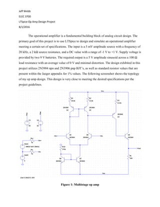
  • 1. Jeff Webb ELEC 3700 LTSpice Op Amp Design Project 8/1/2016 The operational amplifier is a fundamental building block of analog circuit design. The primary goal of this project is to use LTSpice to design and simulate an operational amplifier meeting a certain set of specifications. The input is a 5 mV amplitude source with a frequency of 20 kHz, a 2 kΩ source resistance, and a DC value with a range of -1 V to +1 V. Supply voltage is provided by two 9 V batteries. The required output is a 5 V amplitude sinusoid across a 100 Ω load resistance with an average value of 0 V and minimal distortion. The design exhibited in this project utilizes 2N3904 npn and 2N3906 pnp BJT’s, as well as standard resistor values that are present within the Jaeger appendix for 1% values. The following screenshot shows the topology of my op amp design. This design is very close to meeting the desired specifications per the project guidelines. Figure 1: Multistage op amp
  • 2. The first functional block that will be discussed is the differential input stage given in the figure below. Figure 2: Differential input stage with current mirror load The differential input stage forms the backbone of the op amp circuit. This stage is a bipolar differential amplifier with two npn transistors and an active current mirror load formed from a pnp current mirror as shown. The current mirror is used to enhance the voltage gain capability while helping to maintain the operating point balance that is necessary for good common-mode rejection. The current mirror circuit given below is formed by two npn transistors and a Rref resistor. Figure 3: Current mirror circuit
  • 3. Current mirror biasing is extremely important in this design. A reference current is established by using resistor Rref that provides operating bias to the current mirror. A large value of resistance is required to achieve a small operating current that is independent of the supply voltage. Lastly, the last two stages of the op amp shown below are discussed. Figure 4: pnp common-emitter stage and npn output stage An op amp usually requires higher voltage gain than is available from a single differential amplifier stage. To achieve a higher gain, a pnp common-emitter amplifier Q3 is added by connecting it to the output of the differential amplifier. The resistor R3 is added at the collector of the pnp to help obtain a better output signal centered at 0 V. The output stage Q4 is added to maintain unity voltage gain and provide low output resistance. The input resistance is set by the input differential pair, and the output resistance is determined by the resistance looking into the emitter of Q4.
  • 4. I measured the differential and common mode gain of my op amp using LTSpice. For the differential mode gain, I wired a voltage source to the two inputs of the op amp and specified a voltage of 1 V AC. Next, I ran an AC analysis simulation to obtain the Bode plot shown below. Figure 5: Circuit schematic and Bode plot corresponding to differential mode response In order to measure the common mode gain, I shorted the two input terminals of my op amp and wired it to the positive terminal of a 1 V AC voltage source. Next, I ran an AC analysis simulation to obtain the common mode response shown below. Figure 6: Circuit schematic and Bode plot corresponding to common mode response
  • 5. I also measured total quiescent power dissipation and DC operating points for -1, 0, and +1 V in LTSpice. These values are easily found by running the op amp, hovering the cursor over the output and reading the values at the bottom of the screen. Given below is a table summarizing all of the aforementioned and required quantities for my op amp: DC input Differential Mode Gain Common Mode Gain CMRR Dissipated Power DC Output -1 V 2511 v/v .05 v/v 94 dB 982.4 mW 911.4 mV 0 V 2511 v/v .05 v/v 94 dB 993.3 mW 966.5 mV +1 V 2511 v/v .05 v/v 94 dB 982.4 mW 911.4 mV The following screenshots show plots of the output of my op amp at DC values of 0, -1, and +1 V. Figure 7: Output at 0 V DC
  • 6. Figure 8: Output at -1 V DC Figure 9: Output at +1 V DC Figure 10: Average value of output waveform
  • 7. The results in each plot give an output waveform with an amplitude of about 5.1 V with minimum distortion and an average value of 480.89 mV. This is as close as I could get to the required output amplitude of 5 V with 0 V average value. I think this is a good op amp and I am pleased with this design. It provides good overall characteristics: desired gain, CMRR and good frequency response. Overall, this project has taught me a great deal about the behavior and characteristics of multistage amplifiers. I am confident that the knowledge and experience I have gained from this project will stimulate my future endeavors next semester in radio lab.