More Related Content
Similar to Designing and testing CMOS image sensors
Similar to Designing and testing CMOS image sensors (20)
More from Iaetsd Iaetsd (20)
Designing and testing CMOS image sensors
- 1. Designing of CMOS-IMAGE sensor test-chip
and its characterization
1
Hemalatha K V, Chidananda Murthy M V, M Z
Kurian
1
Department of Electronics and Communication
1
Sri Siddhartha Institute of Technology
Tumakuru, India
1
hemalatha2391@gmail.com
2
Amit Maji
2
Department of Sun Sensor Development
2
Laboratory for Electro Optics Sensors – Indian Space
Research Organization
Bengaluru, India
Abstract: CMOS imagers have extensive applications
ranging from scientific and space applications to
consumer electronics and machine vision system. This
necessitates the development of imagers with low price,
low power consumption, light weight and highly
integrated functions. Among all the imager
technologies, CMOS imager technology emerges and
becomes the candidate that fulfills the power and
integration requirement.
I. INTRODUCTION
Complementary Metal Oxide
Semiconductor(CMOS) sensors became a viable
alternative in the early 1990s. Because of the differences
between the two technologies CCD sensors are likely to
continue to co-exist with CMOS sensors, as the
disadvantages of one are normally the advantages of the
other. This test result of CMOS imager test chip packaged
in CQFZ-100 package. The analog input image is
detected using detector and the output is in the form of
digital.
This test result of CMOS imager test chip SC19001-
0 packaged in CQFZ-100 package. The analog input
image is detected using detectorand the output is in the
form of digital.
The real time image detection algorithm is the most
challenging job in development of image detectors. We
have developed the real time image algorithm and
simulated in Microsemi.
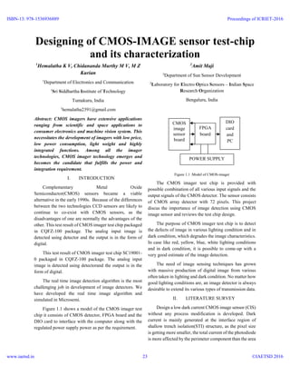
Figure 1.1 shows a model of the CMOS imager test
chip it consists of CMOS detector, FPGA board and the
DIO card to interface with the computer along with the
regulated power supply power as per the requirement.
Figure 1.1 :Model of CMOS-imager
The CMOS imager test chip is provided with
possible combination of all various input signals and the
output signals of the CMOS detector. The sensor consists
of CMOS array detector with 72 pixels. This project
discus the importance of image detection using CMOS
image sensor and reviews the test chip design.
The purpose of CMOS imager test chip is to detect
the defects of image in various lighting condition and in
dark condition, which degrades the image characteristics.
In case like red, yellow, blue, white lighting conditions
and in dark condition, it is possible to come-up with a
very good estimate of the image detection.
The need of image sensing techniques has grown
with massive production of digital image from various
often taken in lighting and dark condition. No matter how
good lighting conditions are, an image detector is always
desirable to extend its various types of transmission data.
II. LITERATURE SURVEY
Design a low dark current CMOS image sensor (CIS)
without any process modification is developed. Dark
current is mainly generated at the interface region of
shallow trench isolation(STI) structure, as the pixel size
is getting more smaller, the total current of the photodiode
is more affected by the perimeter component than the area
CMOS
image
sensor
board
POWER SUPPLY
FPGA
board
DIO
card
and
PC
ISBN-13: 978-1536936889
www.iaetsd.in
Proceedings of ICRIET-2016
©IAETSD 201623
- 2. one. Proposed pixel reduces the dark current effectively
by separating the STI region from the photodiode
junction using simple layout modification and is
characterized.
With minimum process modification, a low dark
current 3 transistors (3T) pixel has been developed. Also
without any process modification, a low dark current 3T
pixel using n+ ring reset was reported. They overlap
capacitance between the reset ring gate and the
photodiode[1].
3T-based low dark current pixel without any process
modification and without sacrifice of conversion gain.
Proposed pixel is implemented using simple layout
modification, measurement results of test image sensors
that adopt proposed pixels show a superior dark current
characteristic without any other significant performance
degradation.
The system is developed and fabricated in 0.6µm
technology to find the minimum detectable signal of the
system in dark and under illumination, an accurate noise
analysis is performed to identify the main dominant noise
sources.
This proposed sensor contains 4x4 matrix of PPS
together with an integrated operational added on the serial
output. To provide an improved adaptability with respect
to operating condition, the PPS matrix can operate in
three modes, which are the reset, the charge integration
and the trans-impedance mode. The PPS matrix operates
in two modes (trans impedance and integration), with a
reset phase after the readout of each pixel, just before the
next pixel readout. Noise analysis is carried out during
three operating modes separately[2].
Designs CMOS image sensor for the dark current
over the temperature range of 295 to 340K and exposure
time of 0 to 500ms. One source results in hot pixels with
high but contrast count for exposure times smaller than
the frame time. The system is designed to decrease the
generation of dark current, many camera systems are
cooled. A cooling system is not feasible and dark current
can become a problem even for small exposure. The
proposed system verified the applicability of the image
correction algorithm to commercially available CMOS
sensor.
This method presented the data for the dark current
of commercially available CMOS image sensor for
different gain settings and bias offsets over the
temperature range of 295to 340K and exposure time of 0
to 500ms. This analysis of hot pixels shows two different
sources of dark current. One source results in hot pixels
with high but contrast count for exposure times smaller
than the frame time. Other hot pixels exhibit a linear
increase with exposure time.
The hot pixels are used to calculate the dark current
for all pixels. Finally he showed that for low bias settings
with universally zero counts for the dark frame one still
needs to correct for dark current. The correction for
thermal noise can therefore result in dark frames with
negative pixel values.
The present imaging performance of color CMOS
sensors reported to be inferior compare to high end CCD
sensors due to excessive dark current, gain non-
uniformity, pixel cross-talk. However, for many cameras
the exact chip temperature is not precisely known. This
proposed dark current correction method requires no
knowledge of the real chip temperature. For a given
exposure time, the dark current of every pixel is
characterized for a specific temperature[3].
Image noise detection and reduction in
complementary metal oxide semiconductor (CMOS)
image sensors inspired from audio noise cancelling
techniques. Digital still and video camera equipped with
CMOS image sensors are well-known to be prone to
noise phenomena, especially in poor lighting dim
environments.
This method typically considered two various
sources of noise namely, white noise and the colored
noise. Noise sources occurred either at the pixel circuitry
level or in the analog-to-digital converter (ADC) unit.
Adaptive filtering method is used for measuring and
attenuating white noise at the pixel level. That is, filtering
method is performed at each pixel based on the
autocorrelation function (ACF) for detecting and
qualifying the amount of white noise.
The system is well suited for high quality imaging
system as it effectively attenuates the amount of white
noise in images, especially in low lighting challenging
environments, a careful inspection shows that there
wereno quality discontinuities nor edge halation
phenomenon. Hence the adaptive filter yields an effective
solution for dealing and correction of white noise on
CMOS camera system, and contributed to high quality
imaging systems[4].
ISBN-13: 978-1536936889
www.iaetsd.in
Proceedings of ICRIET-2016
©IAETSD 201624
- 3. III. SYSTEM DESIGN
The proposed system design block diagram gives the
detected image from various lighting and dark input
conditions. After resulting the output, characterization of
output data is calculated using various characterization
parameters. Figure 3.1 shows the block diagram for chip
designing of CMOS-imager and brief explanation of each
module is given below.
Figure 3.1 : Block diagram for CMOS-imager test-chip
Initially the driver clock signal is given to the
CMOS-imager as an input and the frame, line rate of the
image is defined by using VHDL coding. The coded data
is uploaded to FPGA board and is given to the imager
board for processing. The image is detected by the imager
and the output data signal for classification is seen using
digital oscilloscope.
3.1 CMOS-imager board
It is the basic PCB which consists of CMOS-imager.
The PCB circuit schematic is done using OrCAD
software tool. The circuit layout consists of regulator,
separate analog and digital decoupling capacitor circuit
bank, 100 pin CMOS-imager IC, 50-pin adaptor and the
TP’s.
The layout is for schematic is generated using
CADstar which is an interactive software tool. This
facilitates to generate multiple layer PCB. The
components are placed on the top and bottom layers
respectively.
3.2 Clock driver signal
The driver clock signal of 100KHz is generated using
a software Libero IDE v9.1tool using VHDL coding and
is simulated using Microsemi tool.
3.3 FPGA board
FPGA board for detector drive signal generation
have been wired and tested. FPGA code is written in
VHDL language in Actel Libero IDE software.
All the input-output pins of FPGA are assigned
according to the pin details as shown in Figure 3.2,
commit and check is selected to verify the pin
assignments.
Figure3.2:Pin assignment
The programming device is plugged in, recognized
and enabled. Selecting the “Program” icon in the
FlashPro screen fuses the code into the target device
IV. SYSTEM IMPLEMENTATION
The ADC is placed within the pixel, then the pixel is
classed as a Digital Pixel Sensor (DPS). In the last few
years, work has been carried out which has pioneered this
design, resulting in an increase in the frame rate of the
sensor. The advantage is that the ADCs can operate in
parallel, meaning that digital data is stored in the memory
and read directly from the array, eliminating analogue
A/D conversion and readout bottlenecks. However, these
are still very much in the development stage and APS
pixels are still the predominant pixels being used.
The MOS array can only carry one signal at a time
on each column line; consequently each pixel in a column
must be read out separately. This requires a row select
device in the pixel; when a row is read out all the other
rows are disconnected from the column line. The outputs
from all pixels in a row become available simultaneously,
however if only one output circuit is available for the
entire array, the output columns must also be multiplexed
to one output.
The PCB layout for CMOS-imager board is done in
four layers using CADstar software tool and is fabricated.
ISBN-13: 978-1536936889
www.iaetsd.in
Proceedings of ICRIET-2016
©IAETSD 201625
- 4. The CMOS-imager IC of 100 pin is placed on the imager
board. The imager board of the proposed system is
implemented and it consists of 100KHz clock drive
signal, frame rate.
The PCB layout is fabricated as analog and digital
power supply, analog and digital ground respectively in
four different layers. Components are placed at the top
and bottom layers of the Printed Circuit Board
respectively.
The proposed system consists of two boards in which
one board is to place CMOS-imager for detection and the
other board is of FPGA, it consists of ADC and other
inbuilt operations.
The Detector PCB and FPGA board for detector
drive signal generation have been wired and tested. The
drive signal and processing of detector and ADC
operation are carried out using Actel M1A3P1000
reprogrammable FPGA. The detector analog output is
converted to digital output using ADC128S and
processed by FPGA. The detector full frame digital data
is transferred to the PC using high speed ADLINK
PCI7300A data acquisition card. All pixel data is stored
in to the PC for further processing using software.
V. RESULT
The multi-layer fabricated PCB is wired and the card
is tested for working. DC supply is given to the board and
is tested with Re-programmable FPGA using VHDL code
simulation. Mechanical housing is done and is delivered
to project.
The imager mounted on the card which provides
power supply and biases. Theanalog and digital supplies
are separately decoupled using decoupling capacitors
while designing the PCB. The light is made to fall on the
CMOS-imager mounted on the Printed Circuit
Board(PCB).
The power 3.3V and 1.8V was supplied by lab
supply. Digital Oscilloscope (Tektronix, DPO7254C)
was used to capture a frame of the imager and various
waveforms. Oscilloscope captures FRAME, DATA,
CLOCK and OUTFPA at 100KHz imager clock
frequency. Further the image was extracted from using
computer software. The test setup is shown in the Figure
5.1.
Figure 5.1: Test setup of CMOS detector
Simulation and synthesis are the two main kinds of
tools which operate on the VHDL language. The VHDL
coding for frame, line, data, reset and clock signals are
generated respectively. The code is simulated with proper
test vector.
Power supply
CMOS-imager board
FPGA
board
DIO cable
CMOS-imager
ADC
24MHz oscillator
ISBN-13: 978-1536936889
www.iaetsd.in
Proceedings of ICRIET-2016
©IAETSD 201626
- 5. Figure 5.2: Frame, Clock and Line waveforms in digital oscilloscope
The ‘FRAME’ rate should be ‘high for 4CC’, ‘low
for 2600CC’ ‘LINE’ is ‘high for4CC’, ‘low for 33CC’
and ‘INPUT-DATA’ is ‘high for 5CC’, ‘low for 32CC’
and is shown in Figure 5.2.
Electrical characteristics of CMOS-IMAGER:
The pixel of CMOS-imager is characterized by the
parameters like dark current, sensitivity of the device,
power consumption of the imager board, total FPN, full
well capacity. It is shown in the table below. The test is
carried out at complete dark condition and at ambient
light.
Sl No. Parameter Specified result Unit
1. Integration time 0.1 – 10 ms
2. Full frame rate 27 fps
3. Power supply 3.3 V
4. Analog output range 1.23 V
6. Power consumption 150 mW
7. Output range 0.9 V
8. Output swing 0.9 V
9. Well capacity 0.4 Me-
10. Sensitivity 1.8 µV/ e-
4CC 2600CC
4CC
33CC5CC
32CC
FRAME
LINE
INPUT DATA
CLOCK100KHz
ISBN-13: 978-1536936889
www.iaetsd.in
Proceedings of ICRIET-2016
©IAETSD 201627
- 6. 11. Dark current 5 fA
12. Total FPN 1.4 mV
VI. CONCLUSION
The schematic circuit for CMOS imager test chip is
done using OrCAD, PCB layout is generated using
CADstar. The netlist is generated and verified,
component list is generated for the circuit.
The VHDL code is developed for drive signal of
sensor and simulated in VHDL language using
LiberoIDE.The basic functionality of the sensor is tested
with the existing hardware and facility.Control Signals
for the detector was generated by FPGA. Characterization
of CMOS-imager sensor is the future work of the project
work.
REFERENCES
[1] “A low dark current CMOS Imager sensor pixel with
a photodiode structure enclosed by p-well”, june
2005, by Sans-Wook Han, Seong-Jin Kim and Euisik
Yoon.
[2] “Noise characterization of CMOS image sensors”
WSEAS International conference on CIRCUITS, july
2006 by S. Feruglio.
[3] “Dark current measurement in a CMOS imager”,
International journal for science and emerging
technologies with latest trends, volume 2, 2012, by
AmandeepKaur.
[4] “Digital imaging system testing and design using
physical Sensor characteristics” university of
southern California, December 2009, by Brent
mccleary.
[5] “Fundamentals of Image Sensor Performance”
conference paper, February 2011, by Timothy York.
[6] “Analysis of Total Dose-Induced Dark Current in
CMOS Image Sensors” paper for Interface State
andTrapped Charge Density Measurements, 2009, by
C.Virmontois.
ISBN-13: 978-1536936889
www.iaetsd.in
Proceedings of ICRIET-2016
©IAETSD 201628
![one. Proposed pixel reduces the dark current effectively
by separating the STI region from the photodiode
junction using simple layout modification and is
characterized.
With minimum process modification, a low dark
current 3 transistors (3T) pixel has been developed. Also
without any process modification, a low dark current 3T
pixel using n+ ring reset was reported. They overlap
capacitance between the reset ring gate and the
photodiode[1].
3T-based low dark current pixel without any process
modification and without sacrifice of conversion gain.
Proposed pixel is implemented using simple layout
modification, measurement results of test image sensors
that adopt proposed pixels show a superior dark current
characteristic without any other significant performance
degradation.
The system is developed and fabricated in 0.6µm
technology to find the minimum detectable signal of the
system in dark and under illumination, an accurate noise
analysis is performed to identify the main dominant noise
sources.
This proposed sensor contains 4x4 matrix of PPS
together with an integrated operational added on the serial
output. To provide an improved adaptability with respect
to operating condition, the PPS matrix can operate in
three modes, which are the reset, the charge integration
and the trans-impedance mode. The PPS matrix operates
in two modes (trans impedance and integration), with a
reset phase after the readout of each pixel, just before the
next pixel readout. Noise analysis is carried out during
three operating modes separately[2].
Designs CMOS image sensor for the dark current
over the temperature range of 295 to 340K and exposure
time of 0 to 500ms. One source results in hot pixels with
high but contrast count for exposure times smaller than
the frame time. The system is designed to decrease the
generation of dark current, many camera systems are
cooled. A cooling system is not feasible and dark current
can become a problem even for small exposure. The
proposed system verified the applicability of the image
correction algorithm to commercially available CMOS
sensor.
This method presented the data for the dark current
of commercially available CMOS image sensor for
different gain settings and bias offsets over the
temperature range of 295to 340K and exposure time of 0
to 500ms. This analysis of hot pixels shows two different
sources of dark current. One source results in hot pixels
with high but contrast count for exposure times smaller
than the frame time. Other hot pixels exhibit a linear
increase with exposure time.
The hot pixels are used to calculate the dark current
for all pixels. Finally he showed that for low bias settings
with universally zero counts for the dark frame one still
needs to correct for dark current. The correction for
thermal noise can therefore result in dark frames with
negative pixel values.
The present imaging performance of color CMOS
sensors reported to be inferior compare to high end CCD
sensors due to excessive dark current, gain non-
uniformity, pixel cross-talk. However, for many cameras
the exact chip temperature is not precisely known. This
proposed dark current correction method requires no
knowledge of the real chip temperature. For a given
exposure time, the dark current of every pixel is
characterized for a specific temperature[3].
Image noise detection and reduction in
complementary metal oxide semiconductor (CMOS)
image sensors inspired from audio noise cancelling
techniques. Digital still and video camera equipped with
CMOS image sensors are well-known to be prone to
noise phenomena, especially in poor lighting dim
environments.
This method typically considered two various
sources of noise namely, white noise and the colored
noise. Noise sources occurred either at the pixel circuitry
level or in the analog-to-digital converter (ADC) unit.
Adaptive filtering method is used for measuring and
attenuating white noise at the pixel level. That is, filtering
method is performed at each pixel based on the
autocorrelation function (ACF) for detecting and
qualifying the amount of white noise.
The system is well suited for high quality imaging
system as it effectively attenuates the amount of white
noise in images, especially in low lighting challenging
environments, a careful inspection shows that there
wereno quality discontinuities nor edge halation
phenomenon. Hence the adaptive filter yields an effective
solution for dealing and correction of white noise on
CMOS camera system, and contributed to high quality
imaging systems[4].
ISBN-13: 978-1536936889
www.iaetsd.in
Proceedings of ICRIET-2016
©IAETSD 201624](data:image/gif;base64,R0lGODlhAQABAIAAAAAAAP///yH5BAEAAAAALAAAAAABAAEAAAIBRAA7)