
Recommended
More Related Content
What's hot
What's hot (20)
Similar to Ee8661 ped lab set-1
Similar to Ee8661 ped lab set-1 (20)
Recently uploaded
Recently uploaded (20)
Ee8661 ped lab set-1
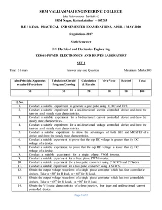
- 1. Page 1 of 2 SRM VALLIAMMAI ENGINEERING COLLEGE (An Autonomous Institution) SRM Nagar, Kattankulathur – 603203 B.E / B.Tech. PRACTICAL END SEMESTER EXAMINATIONS, APRIL / MAY 2020 Regulations-2017 Sixth Semester B.E Electrical and Electronics Engineering EE8661-POWER ELECTRONICS AND DRIVES LABORATORY SET 1 Time: 3 Hours Answer any one Question Maximum Marks:100 Aim/Principle/Apparatus required/Procedure Tabulation/Circuit/ Program/Drawing Calculation & Results Viva-Voce Record Total 30 30 20 10 10 100 Q.No. 1. Conduct a suitable experiment to generate a gate pulse using R, RC and UJT. 2. Conduct a suitable experiment for a uni-directional current controlled device and draw the turn-on and steady state characteristics. 3. Conduct a suitable experiment for a bi-directional current controlled device and draw the steady state characteristics. 4. Conduct a suitable experiment for a uni-directional voltage controlled device and draw the turn-on and steady state characteristics. 5. Conduct a suitable experiment to show the advantages of both BJT and MOSFET of a device and draw the steady state characteristics. 6. Conduct a suitable experiment to prove that the o/p DC voltage is greater than i/p DC voltage of a device. 7. Conduct a suitable experiment to prove that the o/p DC voltage is lesser than i/p DC voltage of a device. 8. Conduct a suitable experiment for a single phase PWM inverter. 9. Conduct a suitable experiment for a three phase PWM inverter. 10. Conduct a suitable experiment for a two pulse converter using 2 SCR’S and 2 Diodes. 11. Conduct a suitable experiment for a two pulse converter using 4 SCR’S. 12. Obtain the output voltage waveform of a single phase converter which has four controllable devices. Take α =300 for R load, α = 600 for R Load. 13. Obtain the output voltage waveform of a single phase converter which has two controllable devices. Take α = 650 for R Load, α =900 for R load. 14. Obtain the V-I static characteristics of a three junction, four layer and unidirectional current controlled device.
- 2. Page 2 of 2 15. Obtain the V-I static characteristics of a three terminal bidirectional current controlled device. 16. Obtain the transfer and output characteristics of a unipolar voltage controlled device. 17. Draw the output waveforms of a buck- boost converter by conducting suitable experiment. 18. Conduct a suitable experiment for an Ac Voltage controller. 19. Conduct a suitable experiment for a Switched mode power converter. 20. Simulate and obtain the output waveform for a 1Φsemiconverter & 3Φsemiconverter model. 21. Simulate and obtain the output waveform for a 1Φfullconverter & 3Φfullconverter model. 22. Simulate and obtain the output waveform for a dc-dc converters & ac voltage controller model. 23. Obtain the V-I static characteristics of a Gate Turn-off thyristor device. 24. Obtain the V-I static characteristics of an Integrated Gate-Commutated Thyristor (IGCT) device. 25. Conduct a suitable experiment for a PMBLDC motor. INTERNAL EXAMINER EXTERNAL EXAMINER