
Recommended
More Related Content
What's hot
What's hot (20)
Similar to TEM.pptx
Similar to TEM.pptx (20)
Recently uploaded
Recently uploaded (20)
TEM.pptx
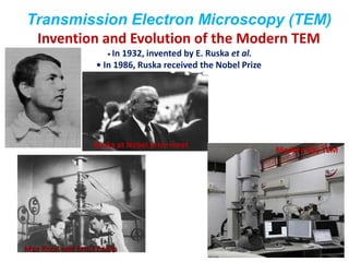
- 1. Transmission Electron Microscopy (TEM) Invention and Evolution of the Modern TEM • In 1932, invented by E. Ruska et al. • In 1986, Ruska received the Nobel Prize Ruska at Nobel prize meet Max Knoll and Ernst Ruska Modern day TEM
- 2. Milestones in the History of Electron Microscopy • 1897 Discovery of the electron by J.J. Thompson • 1924 P. De Broglie: particle/wave dualism • 1927 Hans Busch: Electron beams can be focused in an inhomogeneous magnetic field • 1931 Max Knoll and Ernst Ruska built the first TEM • 1938 Scanning transmission electron microscope (M. von Ardenne) • 1939 First commercial TEM by Siemens (Ruska, von Borries) • 1943 Electron energy-loss spectroscopy EELS (J. Hillier) • ~1940 Basic theoretical work on electron optics and electron lenses (W. Glaser, O. Scherzer) • 1951 X-ray spectroscopy (R. Castaing) • 1956 First lattice image (J. Menter) • 1957 Multi-slice method (J. Cowley, A. Moodie) • 1964 First commercial SEM by Cambridge Instruments • ~1970 HRTEM microscopes with a resolution better than 4 Å • 1986 Nobel prize for E.Ruska (together with G. Binning and H. Rohrer, who developed the Scanning Tunneling Microscope)
- 3. What we covered on electron microscopy 1. Difference between Electron Microscope and Optical Microscope 2. Basic Working principle of SEM and analysis of SEM images 3. Outcomes of SEM images analysis During this discussion we have covered 1. Why electrons 2. How we define resolution and magnification 3. EM lenses Because of these differences, the microscope construction will also be different What we to covered in TEM 1. Difference between SEM, TEM, and HRTEM 2. Basic difference between XRD and SAED (Selected Area Electron Diffraction pattern) 3. Basic Working principle of TEM (including the basic components), sample preparation and different imaging modes 4. Analysis of TEM images 5. Major outcomes of TEM analysis of a specimen
- 4. Why Electrons? In the expression for the resolution (Rayleigh’s Criterion) r = 0.61 /n sin -wavelength, =[1.5/(V+10-6V2)]1/2 nm V-accelerating voltage, n-refractive index -aperture of objective lens, very small in TEM sin and so r=0.61/ ~0.1 radians Green Light 200kV Electrons ~400nm ~0.0025nm n~1.7 oil immersion n~1 (vacuum) r~150nm (0.15m) r~0.02nm (0.2Å) Resolution Limited by Lens Aberrations
- 5. Types of Electron Microscope Transmission Electron Microscope (TEM) uses a wide beam of electrons passing through a thin sliced specimen to form an image. This microscope is analogous to a standard upright or inverted light microscope Scanning Electron Microscope (SEM) uses focused beam of electrons scanning over the surface of thick or thin specimens.. Images are produced one spot at a time in a grid-like raster pattern. (secondary electrons generated due to elastically scattered electrons) High Resolution Transmission Electron Microscope (HRTEM) uses both the transmitted and the scattered beams to create an interference image. It is a phase contrast image and can be as small as the unit cell of crystal. HRTEM has used for analysing crystal structures and lattice imperfections in various kinds of advanced materials on an atomic resolution scale. It can be used for the characterization of point defects, stacking faults, dislocations, precipitates grain boundaries, and surface structures.
- 7. What is a Transmission Electron Microscope (TEM)? Electrons pass through a (very thin) sample (i.e. are transmitted) to form an image. Simplistically, in its operation a TEM can be thought of as analogous to a slide projector:- slide Objective lens Condenser lens Light source Slide projector Projection screen Fluorescent screen Objective lens Condenser lens Specimen (thin) aperture Electron source Electron beam TEM
- 8. •In a slide projector white light from the bulb is focussed onto the slide by a condenser lens. •This produces an image which is focussed by the objective lens to a point (crossover). • The image is then projected onto a screen and magnified by varying the distance from the crossover to the screen. •In a TEM the electron beam is focussed on the sample using the condenser lens system. •This produces an image which is focussed by the objective lens to a point (crossover). •This image is then magnified by a series of projector lenses to vary the size of the image on a fluorescent screen. •Changing the current of an electromagnetic lens alters its focal length altering magnification.
- 9. •TEMs’ have basically the same design independent of manufacturer or age:- Anatomy of a TEM Apertures Viewing Screen Electron Gun Condenser lens system Apertures Sample Sample Viewing Screen a) b) c) Examples of Transmission Electron Microscopes, a)Philips EM420 (1980s), b) Cut through Schematic of Philips CM 200 (1990s) and c) JEOL 2100 (2000s) • JEOL 2100 has digital imaging and computer assisted operation.
- 10. The TEM Column • Gun emits electrons • Electric field accelerate • Magnetic (and electric) field control path of electrons • Electron wavelength @ 200KeV 2x10-12 m • Resolution normally achievable @ 200KeV 2 x 10⁻¹⁰ m 2Å
- 11. Electron Gun W hairpin LaB6 crystal FEG
- 12. Electron Guns •Two main types of gun – Thermionic and Field Emission. •Thermionic sources produce electrons when heated. •Field emission sources produce electrons when exposed to an intense electric field. •FEG’s give much more brightness than thermionic systems. •FEG’s give a more monochromatic electron source and finer probe (i.e. better resolution). Comparison of the three types of source operating at 100kV
- 14. C1 controls the spot size C2 changes the convergence of the beam Condenser-lens system
- 15. The Condenser System •The Wehnelt (or 2nd anode in a FEG) focuses the beam to a crossover which is accelerated down the column. •The first condenser de-magnifies the crossover to give a smaller point source – this is referred to as C1 or spot size. •The second condenser lens (C2) is used to either converge or spread the beam of illumination on the sample (intensity (Philips) or brightness (JEOL)). •A condenser aperture is placed in the beam path to remove electrons far from the optic axis which would reduce resolution. •The smaller the aperture the better the resolution, but there is an associated decrease in brightness – need to compromise.
- 16. The Sample Preparation •Samples are typically 3mm in diameter and <80µm thick. (it depends) •Sample preparation is tricky and time consuming. •For powders:- •Grindmix the powder in chloroform or reagent grade methanol to create a suspension. •Pipette a drop of suspension onto a support grid with a Carbon film coating. •Solvent will evaporate leaving powder dispersed on the grid. •Allow to dry and observe. Thin films are directly coated on support grids. Copper coated Carbon Coated TEM sample Grids
- 18. Image Formation •All rays from a point in the object are gathered by the lens and converge to a point in the image. •All parallel rays are focused in the focal plane. •The back focal plane of the objective lens contains groupings of rays that have left the object at the same angle. •The back focal plane contains the diffraction pattern of the sample. •Diffraction pattern and image are both formed in the imaging process •The intermediate lens is then focused on either the image plane (for the image), or the back focal plane (for the diffraction pattern). sample Objective lens
- 19. IMAGING MODES In the bright field (BF) mode of the TEM, an aperture is placed in the back focal plane of the objective lens, allowing only the transmitted or direct beam to pass. The diffracted beams are blocked. In this case, diffraction contrast contributes to image formation. Crystalline regions that are oriented so as to strongly diffract intensity away from the transmitted beam will appear dark. In addition, Z-contrast occurs when regions with heavy atoms scatter more of the incident beam and appear darker. Therefore, interpretation of contrast should be done with care. In dark field (DF) images, a selected diffracted beam is allowed to pass through the objective aperture. This is accomplished by electromagnetic lenses that effectively tilt the incident beam from the optical axis by an amount 2θ hkl such that the hkl diffracted beam exits the sample parallel to the TEM optical axis. In contrast to the direct beam, the diffracted beam has interacted strongly with the specimen, and very useful information is often present in DF images, e.g., about planar defects, stacking faults, or particles.
- 20. In many analyses, correlation between DF and BF images provides useful information about structure and morphology, including layer thickness, grain size, grain orientation, and defect orientations. In general, one or both of these imaging modes are used in conjunction with electron diffraction analysis.
- 21. Selected Area Diffraction Similar to BF and DF imaging—an image of the diffracted beams is brought into focus at the back focal plane of the objective lens. Once this real image is formed, it can be projected onto the viewing screen by the intermediate and projection lens system. In many cases, one desires to obtain crystallography information about a specific area of the sample or about a secondary phase present in the sample. For such cases, selected area diffraction (SAD) requires that an intermediate aperture is placed at the first intermediate image focal plane to specify the area from which the diffraction image is acquired. Through use of this method, crystallographic information is obtained from small features and from small volumes of materials such as precipitates.
- 22. Under diffraction conditions, a portion of the incident radiation makes the appropriate angle with a specific set of (hkl) planes such that Bragg’s Law is satisfied . Given that the typical operation wavelength can vary between 0.37 and 0.87 pm, the diameter of the Ewald sphere (ES) is very large when compared with the size of the unit cell in reciprocal space. Hence, near the origin of reciprocal space, the curvature of the ES is so small that it is essentially a plane perpendicular to the direction of the incident radiation. Hence, the ES passes through several points in reciprocal space that satisfy Bragg’s Law. The function of the magnification lenses is to project the image that is in the back focal plane, and that image is a set of points on the surface of the Ewald sphere. The image in fact is a planar section of the reciprocal lattice, perpendicular to the incident radiation.
- 23. A single-crystal sample produces spot patterns associated with a specific zone axis for that crystal. Under diffraction conditions, polycrystalline samples give rise to ring patterns, which are actually the superposition of many single-crystal patterns. In general, correlation between DF and BF images can provide extensive information about structure and morphology, including layer thickness, grain size, grain orientation, and defect orientation. Typically, however, one or both of these imaging modes are used in conjunction with electron diffraction analysis.
- 24. Contrast •Conventionally, in order to get contrast in an image an objective aperture is placed in the beam path at the back focal plane of the objective lens. •Any electrons which are scattered by interaction with the sample are prevented from recombining in the image by the aperture. •Any regions where electrons are scattered will appear dark in the image. •The smaller the aperture used the greater the contrast, but at the expense of brightness. •Another method of achieving contrast is the ‘Mass thickness Contrast’ mechanism. •Thicker (or higher Z) areas of the sample scatter more electrons than thinner (lower Z areas). •Therefore fewer electrons from the dark region fall onto the screen, so the region appears darker in a Bright Field image. Mechanism of mass thickness contrast
- 25. Projection - Magnification •A series of projector lenses are then used to magnify the image formed by the intermediate lens onto a viewing screen. •Electron Microscope lenses are Electro-magnetic in nature. •They consist of a cylindrical soft metal core (polepiece) with a hole drilled through it (bore) wound with copper wire. •When a current is passed through the coils a magnetic field is created in the bore. •Changing the current in the windings changes the magnetic field and effectively changes the focal length of the lens.
- 26. ViewingRecording Images •The image, comprising of a beam of focused electrons falls onto a fluorescent screen therefore producing a visible image. •This image can be recorded onto photographic film using the camera located underneath the viewing screen. •Modern machines can capture images digitally using CCD cameras. •The signal from the beam can be output to external analysis equipment. Digital CCD camera Fluorescent viewing screen
- 27. Indexing Diffraction Patterns (Single-Crystal Diffraction Patterns) Single-crystal diffraction patterns consist of a series of bright spots, with the transmitted beam being the brightest and the others bright spots being the diffracted beams. The first step in the analysis of electron diffraction patterns is to measure the dhkl values. The diffracted beam makes an angle of 2 relative to the direct beam and falls on the screen at a distance R from the transmitted spot. The net effect of the lens settings is encompassed in the camera length (L), which is an effective distance between the sample and the photographic plate (and/or viewing screen). When diffraction spots appear, the Ewald sphere intersects the center spot (i.e., the origin of 1/R space) and also intersects the 1/R-lattice vector d∗ hkl , so Bragg’s Law is satisfied.
- 28. When Bragg’s Law is satisfied during ED, the wavelength is small (∼ tens of picometers) and the Bragg angle is also small (0.5◦). From Figure, tan(2) = R/L Since θ is small, tan(2) ≈ 2 (in radians); this gives us the relationship 2 = R/L . Similarly for Bragg’s Law, sin() ≈ θ and hence λ = 2 dhkl or λ/dhkl = 2. R/L = 2 = λ/dhkl , R dhkl = L λ, where λL is known as the camera constant and (like L) varies with the lens settings in the microscope. The units of the camera constant are typically expressed in units of mm-nm or cm-nm or m-nm, where R is the distance measured on the screen or photographic plate (e.g., mm or cm or m) and dhkl (e.g., nm) is the interatomic spacing of the planes (hkl). The camera constant is a function of the lens settings. It is these lens settings that actually control the optical system’s magnification, and the electron energy determines the value of the wavelength. The accuracy of the calculated dhkl is limited by uncertainty in the diffraction spot positions and of the camera constant. The diffraction spots are often diffuse, and hence the determination of the center position is an approximation. The camera constant is used to determine a known standard sample for a given electron energy setting. The resulting diffraction pattern is indexed, and the calculated camera constant is loaded into the microscope’s memory.
- 29. For diffraction in electron microscope: The single crystal electron diffraction pattern is a series of spots equivalent to a magnified view of a planar section through the reciprocal lattice normal to the incident beam. specimen Ewald sphere 1/ Camera Length (L) r r rdhkl=L, L - camera constant
- 30. Indexing the SAED pattern (spot pattern): h1k1l1 h2k2l2 h3k3l3 1 2 R3 R1 R2
- 31. Measure R values for at least three reflections
- 32. Index other reflections by vector sums, differences Next find zone axis from cross product of any two (hkl)s (202) x (220) ——> [4̄44] ——> [1̄11]
- 33. Ring pattern: The reciprocal lattice becomes a series of sphere concentric with the origin of the reciprocal lattice. beam O hkl sphere D The main steps of indexing ring patterns: 1) Measuring ring diameters D1, D2, D3 ……. 2) Calculation of the dhkl (using the expression: rdhkl=L) 3) Use some structure database to index each ring.
- 34. SAED Patterns of Single Crystal, Polycrystalline and Amorphous Samples a b c a. Single crystal Fe (BCC) thin film-[001] a. Polycrystalline thin film of Pd2Si b. Amorphous thin film of Pd2Si. The diffuse halo is indicative of scattering from an amorphous material. SAED Patterns of Single Crystal, Polycrystalline and Amorphous Samples a. Single crystal Fe (BCC) thin film-[001] b. Polycrystalline thin film of Pd2Si c. Amorphous thin film of Pd2Si. The diffuse halo is indicative of scattering from an amorphous material.
- 35. Comparison of SAED and XRD a. Similarities (Arrangement and function of components are similar) 1) Illumination system: produces required radiation and directs it onto the specimen. Consists of a source, which emits the radiation, and a condenser lens, which focuses the illuminating beam (allowing variations of intensity to be made) on the specimen. 2) Specimen stage: situated between the illumination and imaging systems. 3) Imaging system: Lenses which together produce the final magnified image of the specimen. Consists of i) an objective lens which focuses the beam after it passes through the specimen and forms an intermediate image of the specimen and ii) the projector lens(es) which magnifies a portion of the intermediate image to form the final image. 4) Image recording system: Converts the radiation into a permanent image (typically on a photographic emulsion) that can be viewed.
- 36. b. Differences 1) Optical lenses are generally made of glass with fixed focal lengths whereas magnetic lenses are constructed with ferromagnetic materials and windings of copper wire producing a focal length which can be changed by varying the current through the coil. 2) Magnification in the LM is generally changed by switching between different power objective lenses mounted on a rotating turret above the specimen. It can also be changed if oculars (eyepieces) of different power are used. In the TEM the magnification (focal length) of the objective remains fixed while the focal length of the projector lens is changed to vary magnification. 3) The LM has a small depth of field, thus different focal levels can be seen in the specimen. The large (relative) depth of field in the TEM means that the entire (thin) specimen is in focus simultaneously. 4) Mechanisms of image formation vary (phase and amplitude contrast). 5) TEMs are generally constructed with the radiation source at the top of the instrument: the source is generally situated at the bottom of LMs. 6) TEM is operated at high vacuum (since the mean free path of electrons in air is very small) so most specimens (biological) must be dehydrated (i.e. dead !!). 7) TEM specimens (biological) are rapidly damaged by the electron beam. 8) TEMs can achieve higher magnification and better resolution than LMs. 9) Price tag!!! (100x more than LM)