SlideShare a Scribd company logo
1 of 50
Scale of Structure Organization
X-Ray Diffraction (XRD)
Basics of Diffraction
For electromagnetic radiation to be diffracted the spacing in the grating
should be of the same order as the wavelength
 In crystals the typical interatomic spacing ~ 2-3 Å so the suitable radiation
is X-rays
 Hence, X-rays can be used for the study of crystal structures
 Neutrons and Electrons are also used for diffraction studies from materials.
 Neutron diffraction is especially useful for studying the magnetic ordering
in materials
 The three X-ray scattering patterns above were produced by three chemically
identical forms SiO2
 Crystalline materials like quartz and Cristobalite produce X-ray diffraction patterns
– Quartz and Cristobalite have two different crystal structures
–The Si and O atoms are arranged differently, but both have long-range atomic
order
–The difference in their crystal structure is reflected in their different diffraction
patterns
 The amorphous glass does not have long-range atomic order and therefore
produces only broad scattering features
Optical Microscope
Optical microscope is a type of microscope which
uses visible light and a system of lenses to magnify
images of small samples.
There are two basic configurations of the conventional
optical microscope in use, the simple (one lens) and
the compound (many lenses).
Assumptions in Light Theory
1.Light travels in a straight line.
2.Portions of light beams can be treated as
individual rays.
3.Law of reflection.
4.Law of refraction.
Simple Lens
Kirkpatrick/Francis – “Physics; A World View
SPHERICAL SURFACE
Optics of a Microscope
Slide with the letter “F”
The letter “F” as it
appears when
viewed through the
eyepiece
F
Images viewed through the
eyepiece of compound
microscopes will appear
upside-down and
backwards.
How it Works?
Light
source or
Mirror
Optical
Condenser
Light
passes
through the
specimen
Objective
Lenses
(X100)
First Image
Eyepiece
or Ocular
(X10)
Image
(X1000)
Retina
Basic Components
 Eyepiece Lens: the lens at the
top that you look through.
 Tube: Connects the eyepiece to
the objective lenses
 Objective Lenses: Usually you
will find 3 or 4 objective lenses
on a microscope. They almost
always consist of 5X, 10X, 20X ,
50X and 100X powers.
 Rack Stop: This is an
adjustment that determines how
close the objective lens can get
to the slide.
 Condenser Lens: The purpose
of the condenser lens is to focus
the light onto the specimen.
Basic Components
 Stage: The flat platform where you
place your slides. Stage clips hold
the slides in place.
 Revolving Nosepiece or Turret:
This is the part that holds two or
more objective lenses and can be
rotated to easily change power.
 Illuminator: A steady light source
(110 volts) used in place of a mirror.
If your microscope has a mirror, it is
used to reflect light from an external
light source.
 Arm: Supports the tube and
connects it to the base
 Base: The bottom of the
microscope, used for support
Total Magnification
• The total magnification of
the specimen being viewed
is calculated using the
ocular lens multiplied by
the objective lens.
• For example, if the ocular
lens is 10x and the ocular
lens is 50x then the total
magnification would be
500x.
Focusing a Microscope
• Course-adjustment knob- is the
larger of the two knobs. It is used
in bringing the object into quick
focus.
• Fine-adjustment knob- is used for
improving the clarity of the image,
especially when viewing under
high power.
Quality of an Image
• Focal Length
• Size of sample
• Type of sample
• Quality of Microscope and lenses
• Amount of light on the sample
• Quality of sample
Numerical Aperture (NA)
The objective collects as much light as possible coming from any
point on the specimen and combines this light to form the image.
The numerical aperture (NA) is a measure of the light collection
capability of the objective and is defined as 𝑵𝑨 = 𝒏. 𝐬𝐢𝐧 𝜶
Objectives with a shorter focal length have a wider angular aperture and therefore
deliver a higher NA and resolution.
Numerical Aperture (NA)
The objective with the higher numerical aperture is
clearly able to give us more detail with separation
between the wavelets.
https://microscopeclarity.com/what-is-microscope-resolution/
Depth of Field
• The depth of field is the
distance along the optical
axis over which details of
the object can be observed
with adequate sharpness
• "Depth of field" refers to the
thickness of the plane of
focus.
• It is the vertical distance
(from above to below the
focal plane) that yields a
useful image.
The series of images show
how the depth of field can
influence the appearance
of an image.
With narrow
depth of
field, only
part of the
image is in
focus at the
same time.
With a large
depth of field,
the entire
image is in
focus at the
same time.
Depth of Field: Example
Resolution
• Resolution or resolving power is the closest spacing
of two points which can clearly be seen through the
microscope to be separate entities.
• It is not necessarily the same as the smallest point
which can be seen with the microscope, which will
often be smaller than the resolution limit.
• Resolving power, 𝑑 =
0.61𝜆
𝑛.sin 𝛼
=
0.61𝜆
𝑁𝐴
Resolution: Examples
https://microscopeclarity.com/what-is-microscope-resolution/
https://www.cherrybiotech.com/scientific-
note/microscopy/beyond-the-limits-of-light
diffraction-super-resolution-microscopy
https://www.microscope
world.com/t-
camera_resolution.aspx
• Inexpensive
• Easy to learn and operate
• Very sharp plane of focus
• Small and portable
Advantages
• Magnification is limited
• Specimen may be disfigured during preparation to be
viewed under the microscope.
• Only has a resolution of 0.2 μm - which is relatively poor
in comparison to other microscopes.
• Poor surface view
Disadvantages
Allotriomorphic ferrite in a Fe-0.4C
steel which is slowly cooled; the
remaining dark-etching microstructure
is fine pearlite
Optical micrograph showing colonies of
pearlite (courtesy S. S. Babu)
https://www.phase-trans.msm.cam.ac.uk/2008/Steel_Microstructure/SM.html
Microstructure: Examples
Left, as-cast cadmium etched with 2% nital, 30 x ; right, as-cast alloy of Cd and 10% Bi etched
with 2% nital, 60 x .
Microstructure: Examples
Superpure aluminum anodized using the method of Hone and Pearson (Ref. 56),
polarized light, 32 x . Left, held 6 min at 375°C, partly recrystallized. Right, held 2 h at
375°C, fully recrystallized. (Courtesy of E. C. Pearson, Alcan International Ltd.)
Color etching of various grain or mixed-crystal areas and sulphate layers
of different thicknesses
Ferrite-perlite microstructure, the ferrite
is tinted while Fe3C is kept white
Klemm (K) etch
This contrasting visualizes the quality
of a soft annealing (K)
https://www.leica-microsystems.com/science-lab/metallography-with-color-and-contrast/
Microstructure: Examples
Brightfield image of a cast austenite
structure caused by a laser melting
process
Improved contrast using interference
Microstructure: Examples
The same sample in interference contrast
showing clear contrasting of the
dendrites (B)
Klemm (K) etchant: 50 mL saturated aqueous sodium thiosulfate, 1 g potassium metabisulfites
Beraha (B) etchant: (a) Stock solution: 1:2, 1:1, or 1:0.5 HCI-water
(b) 100 mL stock solution plus 0.6-1.0 g potassium metabisulfite
https://www.leica-microsystems.com/science-lab/metallography-with-color-and-contrast/
Scanning Electron Microscopy – (SEM)
Construction of SEM
SEM
Magnification range
15x to 200,000x
Resolution of 50 Å
Excellent depth of
focus
Relatively easy
sample preparation
A brief description of each system follows:
1. Vacuum system. A vacuum is required when using an electron beam because
electrons will quickly disperse or scatter due to collisions with other molecules.
2. Electron beam generation system. This system is found at the top of the
microscope column. This system generates the "illuminating" beam of electrons known
as the primary electron beam.
3. Electron beam manipulation system. This system consists of electromagnetic
lenses and coils located in the microscope column and control the size, shape, and
position of the electron beam on the specimen surface.
4. Beam specimen interaction system. This system involves the interaction of the
electron beam with the specimen and the types of signals that can be detected.
5. Detection system. This system can consist of several different detectors, each
sensitive to different energy / particle emissions that occur on the sample.
6. Signal processing system. This system is an electronic system that processes the
signal generated by the detection system and allows additional electronic manipulation
of the image.
7. Display and recording system. This system allows visualization of an electronic
signal using a cathode ray tube and permits recording of the results using photographic
or magnetic media.
Components of SEM
Principle of SEM image formation
When an electron beam is incident
on the sample then many different
types of signals are generated which
are eventually used to observe or
analyze morphology/ topology of the
sample. SEM is also used for
elemental and state analysis. These
signals includes – Secondary
electrons, Backscattered electrons,
Auger electrons,
Cathodoluminescence and X-rays.
Interaction of Electrons with Specimen: Electrons entering specimen gets
scattered within it and lose their energy gradually upon getting absorbed
within the sample. Scattering range within specimen depends upon-
Energy of electrons – More Energy More Scattering.
Element’s atomic number (Z) making the sample - More Z Less
Scattering.
Density of constituent atoms – More Density less scattering.
SEM Sample-
Conducting samples provide a path to ground for the beam electrons, and therefore
require no special preparation. Insulating materials, however, require a thin coating
of a conductor (often carbon or gold) in order to prevent charging.
Sample Preparation-
It is done in order to eliminate the sample charging few steps are followed:
1. Charging: A thin metal coating of about 10nm is done on the sample because
metal film is highly stable and its secondary electron yield is higher. Too thin coating
is not preferred because continuity is lost.
2. Low accelerating voltage: Low KV value of about 1KV can be used to scan
insulating samples because the number of incident electrons becomes equal to the
number of emitted secondary electrons, implying that the sample is not charged.
3. Tilt Observation: In this case secondary electrons yield is higher as electron
beam is entering at an angle.
4. Low Vacuum SEM observation: Ondecreasing the vacuum, the gas molecules
within the sample chamberincreases, which get ionized due to electrons and thus,
on reaching the specimen as positive ions neutralize the charging.
SEM sample Preparation
Transmission Electron Microscopy – (TEM)
Construction of TEM Instrument components
 Electron gun (described
previously)
 Condenser system (lenses &
apertures for controlling
illumination on specimen)
 Specimen chamber
assembly
 Objective lens system
(image-forming lens - limits
resolution; aperture -
controls imaging conditions)
 Projector lens system
(magnifies image or
diffraction pattern onto final
screen)
dislocations
in superalloy
SiO2 precipitate
particle in Si
Examples
Sample Preparation for TEM
Material Characterization Techniques.pptx

More Related Content

Similar to Material Characterization Techniques.pptx

Chumbley sem
Chumbley semChumbley sem
Chumbley semAn Iron
 
Microscopy fin
Microscopy finMicroscopy fin
Microscopy finMUBOSScz
 
Tunneling electron Microscopy, Scanning electron microscopy
Tunneling electron Microscopy, Scanning electron microscopyTunneling electron Microscopy, Scanning electron microscopy
Tunneling electron Microscopy, Scanning electron microscopyelminehtsegahun2
 
Microscope and types of microscope
Microscope and types of microscopeMicroscope and types of microscope
Microscope and types of microscopeRimsha Pahore
 
Phase Contrast Microscopy - Microbiology 1st
Phase Contrast Microscopy - Microbiology 1st Phase Contrast Microscopy - Microbiology 1st
Phase Contrast Microscopy - Microbiology 1st RAHUL PAL
 
Introduction to microscope
Introduction to microscopeIntroduction to microscope
Introduction to microscopeTasmiaZeb1
 
Electron microscope
Electron microscopeElectron microscope
Electron microscopeReena Rai
 
Microscopy and Microscopic techniques
Microscopy and Microscopic techniquesMicroscopy and Microscopic techniques
Microscopy and Microscopic techniquesAnees Ahmad
 
Electron microscope
Electron microscopeElectron microscope
Electron microscopejakkaas
 

Similar to Material Characterization Techniques.pptx (20)

microscopy
 microscopy microscopy
microscopy
 
Chumbley sem
Chumbley semChumbley sem
Chumbley sem
 
Microscopy
MicroscopyMicroscopy
Microscopy
 
SEM- scanning electron microscope
SEM- scanning electron microscope SEM- scanning electron microscope
SEM- scanning electron microscope
 
Microscope.pptx
Microscope.pptxMicroscope.pptx
Microscope.pptx
 
TEM.pptx
TEM.pptxTEM.pptx
TEM.pptx
 
Microscopy fin
Microscopy finMicroscopy fin
Microscopy fin
 
NDT.pptx
NDT.pptxNDT.pptx
NDT.pptx
 
Tunneling electron Microscopy, Scanning electron microscopy
Tunneling electron Microscopy, Scanning electron microscopyTunneling electron Microscopy, Scanning electron microscopy
Tunneling electron Microscopy, Scanning electron microscopy
 
Electron Microscope
Electron MicroscopeElectron Microscope
Electron Microscope
 
The Microscope
The MicroscopeThe Microscope
The Microscope
 
Microscope and types of microscope
Microscope and types of microscopeMicroscope and types of microscope
Microscope and types of microscope
 
Phase Contrast Microscopy - Microbiology 1st
Phase Contrast Microscopy - Microbiology 1st Phase Contrast Microscopy - Microbiology 1st
Phase Contrast Microscopy - Microbiology 1st
 
Microscopy ii
Microscopy iiMicroscopy ii
Microscopy ii
 
Introduction to microscope
Introduction to microscopeIntroduction to microscope
Introduction to microscope
 
Electron microscope
Electron microscopeElectron microscope
Electron microscope
 
Microscope 120109025117-phpapp02
Microscope 120109025117-phpapp02Microscope 120109025117-phpapp02
Microscope 120109025117-phpapp02
 
Microscopy and Microscopic techniques
Microscopy and Microscopic techniquesMicroscopy and Microscopic techniques
Microscopy and Microscopic techniques
 
Electron microscope
Electron microscopeElectron microscope
Electron microscope
 
Poster
PosterPoster
Poster
 

More from ssuser0cd0f1

09C Processing and Applications of Ceramics (4.5 MB).ppt
09C Processing and Applications of Ceramics (4.5 MB).ppt09C Processing and Applications of Ceramics (4.5 MB).ppt
09C Processing and Applications of Ceramics (4.5 MB).pptssuser0cd0f1
 
Manufacturing Technology of Materials in Engineering
Manufacturing Technology of Materials in EngineeringManufacturing Technology of Materials in Engineering
Manufacturing Technology of Materials in Engineeringssuser0cd0f1
 
3142509_Mechanics_of_Metal_Cutting_1777.pptx
3142509_Mechanics_of_Metal_Cutting_1777.pptx3142509_Mechanics_of_Metal_Cutting_1777.pptx
3142509_Mechanics_of_Metal_Cutting_1777.pptxssuser0cd0f1
 
7 shpaper planer machining of flat surfaces.pdf
7 shpaper planer machining of flat surfaces.pdf7 shpaper planer machining of flat surfaces.pdf
7 shpaper planer machining of flat surfaces.pdfssuser0cd0f1
 
__lec_12_-_13_shaping_planing_and_slotting_operations.pdf
__lec_12_-_13_shaping_planing_and_slotting_operations.pdf__lec_12_-_13_shaping_planing_and_slotting_operations.pdf
__lec_12_-_13_shaping_planing_and_slotting_operations.pdfssuser0cd0f1
 
05) Gating System in CAsting of Materials
05) Gating System in CAsting of Materials05) Gating System in CAsting of Materials
05) Gating System in CAsting of Materialsssuser0cd0f1
 
Material Characterization Techniques.pptx
Material Characterization Techniques.pptxMaterial Characterization Techniques.pptx
Material Characterization Techniques.pptxssuser0cd0f1
 

More from ssuser0cd0f1 (7)

09C Processing and Applications of Ceramics (4.5 MB).ppt
09C Processing and Applications of Ceramics (4.5 MB).ppt09C Processing and Applications of Ceramics (4.5 MB).ppt
09C Processing and Applications of Ceramics (4.5 MB).ppt
 
Manufacturing Technology of Materials in Engineering
Manufacturing Technology of Materials in EngineeringManufacturing Technology of Materials in Engineering
Manufacturing Technology of Materials in Engineering
 
3142509_Mechanics_of_Metal_Cutting_1777.pptx
3142509_Mechanics_of_Metal_Cutting_1777.pptx3142509_Mechanics_of_Metal_Cutting_1777.pptx
3142509_Mechanics_of_Metal_Cutting_1777.pptx
 
7 shpaper planer machining of flat surfaces.pdf
7 shpaper planer machining of flat surfaces.pdf7 shpaper planer machining of flat surfaces.pdf
7 shpaper planer machining of flat surfaces.pdf
 
__lec_12_-_13_shaping_planing_and_slotting_operations.pdf
__lec_12_-_13_shaping_planing_and_slotting_operations.pdf__lec_12_-_13_shaping_planing_and_slotting_operations.pdf
__lec_12_-_13_shaping_planing_and_slotting_operations.pdf
 
05) Gating System in CAsting of Materials
05) Gating System in CAsting of Materials05) Gating System in CAsting of Materials
05) Gating System in CAsting of Materials
 
Material Characterization Techniques.pptx
Material Characterization Techniques.pptxMaterial Characterization Techniques.pptx
Material Characterization Techniques.pptx
 

Recently uploaded

The Most Attractive Pune Call Girls Budhwar Peth 8250192130 Will You Miss Thi...
The Most Attractive Pune Call Girls Budhwar Peth 8250192130 Will You Miss Thi...The Most Attractive Pune Call Girls Budhwar Peth 8250192130 Will You Miss Thi...
The Most Attractive Pune Call Girls Budhwar Peth 8250192130 Will You Miss Thi...ranjana rawat
 
OSVC_Meta-Data based Simulation Automation to overcome Verification Challenge...
OSVC_Meta-Data based Simulation Automation to overcome Verification Challenge...OSVC_Meta-Data based Simulation Automation to overcome Verification Challenge...
OSVC_Meta-Data based Simulation Automation to overcome Verification Challenge...Soham Mondal
 
MANUFACTURING PROCESS-II UNIT-2 LATHE MACHINE
MANUFACTURING PROCESS-II UNIT-2 LATHE MACHINEMANUFACTURING PROCESS-II UNIT-2 LATHE MACHINE
MANUFACTURING PROCESS-II UNIT-2 LATHE MACHINESIVASHANKAR N
 
HARDNESS, FRACTURE TOUGHNESS AND STRENGTH OF CERAMICS
HARDNESS, FRACTURE TOUGHNESS AND STRENGTH OF CERAMICSHARDNESS, FRACTURE TOUGHNESS AND STRENGTH OF CERAMICS
HARDNESS, FRACTURE TOUGHNESS AND STRENGTH OF CERAMICSRajkumarAkumalla
 
(ANJALI) Dange Chowk Call Girls Just Call 7001035870 [ Cash on Delivery ] Pun...
(ANJALI) Dange Chowk Call Girls Just Call 7001035870 [ Cash on Delivery ] Pun...(ANJALI) Dange Chowk Call Girls Just Call 7001035870 [ Cash on Delivery ] Pun...
(ANJALI) Dange Chowk Call Girls Just Call 7001035870 [ Cash on Delivery ] Pun...ranjana rawat
 
High Profile Call Girls Nagpur Isha Call 7001035870 Meet With Nagpur Escorts
High Profile Call Girls Nagpur Isha Call 7001035870 Meet With Nagpur EscortsHigh Profile Call Girls Nagpur Isha Call 7001035870 Meet With Nagpur Escorts
High Profile Call Girls Nagpur Isha Call 7001035870 Meet With Nagpur Escortsranjana rawat
 
Introduction and different types of Ethernet.pptx
Introduction and different types of Ethernet.pptxIntroduction and different types of Ethernet.pptx
Introduction and different types of Ethernet.pptxupamatechverse
 
Sheet Pile Wall Design and Construction: A Practical Guide for Civil Engineer...
Sheet Pile Wall Design and Construction: A Practical Guide for Civil Engineer...Sheet Pile Wall Design and Construction: A Practical Guide for Civil Engineer...
Sheet Pile Wall Design and Construction: A Practical Guide for Civil Engineer...Dr.Costas Sachpazis
 
Call Girls Service Nashik Vaishnavi 7001305949 Independent Escort Service Nashik
Call Girls Service Nashik Vaishnavi 7001305949 Independent Escort Service NashikCall Girls Service Nashik Vaishnavi 7001305949 Independent Escort Service Nashik
Call Girls Service Nashik Vaishnavi 7001305949 Independent Escort Service NashikCall Girls in Nagpur High Profile
 
SPICE PARK APR2024 ( 6,793 SPICE Models )
SPICE PARK APR2024 ( 6,793 SPICE Models )SPICE PARK APR2024 ( 6,793 SPICE Models )
SPICE PARK APR2024 ( 6,793 SPICE Models )Tsuyoshi Horigome
 
(SHREYA) Chakan Call Girls Just Call 7001035870 [ Cash on Delivery ] Pune Esc...
(SHREYA) Chakan Call Girls Just Call 7001035870 [ Cash on Delivery ] Pune Esc...(SHREYA) Chakan Call Girls Just Call 7001035870 [ Cash on Delivery ] Pune Esc...
(SHREYA) Chakan Call Girls Just Call 7001035870 [ Cash on Delivery ] Pune Esc...ranjana rawat
 
KubeKraft presentation @CloudNativeHooghly
KubeKraft presentation @CloudNativeHooghlyKubeKraft presentation @CloudNativeHooghly
KubeKraft presentation @CloudNativeHooghlysanyuktamishra911
 
CCS335 _ Neural Networks and Deep Learning Laboratory_Lab Complete Record
CCS335 _ Neural Networks and Deep Learning Laboratory_Lab Complete RecordCCS335 _ Neural Networks and Deep Learning Laboratory_Lab Complete Record
CCS335 _ Neural Networks and Deep Learning Laboratory_Lab Complete RecordAsst.prof M.Gokilavani
 
VIP Call Girls Service Hitech City Hyderabad Call +91-8250192130
VIP Call Girls Service Hitech City Hyderabad Call +91-8250192130VIP Call Girls Service Hitech City Hyderabad Call +91-8250192130
VIP Call Girls Service Hitech City Hyderabad Call +91-8250192130Suhani Kapoor
 
UNIT-V FMM.HYDRAULIC TURBINE - Construction and working
UNIT-V FMM.HYDRAULIC TURBINE - Construction and workingUNIT-V FMM.HYDRAULIC TURBINE - Construction and working
UNIT-V FMM.HYDRAULIC TURBINE - Construction and workingrknatarajan
 
High Profile Call Girls Nagpur Meera Call 7001035870 Meet With Nagpur Escorts
High Profile Call Girls Nagpur Meera Call 7001035870 Meet With Nagpur EscortsHigh Profile Call Girls Nagpur Meera Call 7001035870 Meet With Nagpur Escorts
High Profile Call Girls Nagpur Meera Call 7001035870 Meet With Nagpur EscortsCall Girls in Nagpur High Profile
 
Call for Papers - African Journal of Biological Sciences, E-ISSN: 2663-2187, ...
Call for Papers - African Journal of Biological Sciences, E-ISSN: 2663-2187, ...Call for Papers - African Journal of Biological Sciences, E-ISSN: 2663-2187, ...
Call for Papers - African Journal of Biological Sciences, E-ISSN: 2663-2187, ...Christo Ananth
 
Call Girls in Nagpur Suman Call 7001035870 Meet With Nagpur Escorts
Call Girls in Nagpur Suman Call 7001035870 Meet With Nagpur EscortsCall Girls in Nagpur Suman Call 7001035870 Meet With Nagpur Escorts
Call Girls in Nagpur Suman Call 7001035870 Meet With Nagpur EscortsCall Girls in Nagpur High Profile
 
Introduction to Multiple Access Protocol.pptx
Introduction to Multiple Access Protocol.pptxIntroduction to Multiple Access Protocol.pptx
Introduction to Multiple Access Protocol.pptxupamatechverse
 
UNIT-III FMM. DIMENSIONAL ANALYSIS
UNIT-III FMM.        DIMENSIONAL ANALYSISUNIT-III FMM.        DIMENSIONAL ANALYSIS
UNIT-III FMM. DIMENSIONAL ANALYSISrknatarajan
 

Recently uploaded (20)

The Most Attractive Pune Call Girls Budhwar Peth 8250192130 Will You Miss Thi...
The Most Attractive Pune Call Girls Budhwar Peth 8250192130 Will You Miss Thi...The Most Attractive Pune Call Girls Budhwar Peth 8250192130 Will You Miss Thi...
The Most Attractive Pune Call Girls Budhwar Peth 8250192130 Will You Miss Thi...
 
OSVC_Meta-Data based Simulation Automation to overcome Verification Challenge...
OSVC_Meta-Data based Simulation Automation to overcome Verification Challenge...OSVC_Meta-Data based Simulation Automation to overcome Verification Challenge...
OSVC_Meta-Data based Simulation Automation to overcome Verification Challenge...
 
MANUFACTURING PROCESS-II UNIT-2 LATHE MACHINE
MANUFACTURING PROCESS-II UNIT-2 LATHE MACHINEMANUFACTURING PROCESS-II UNIT-2 LATHE MACHINE
MANUFACTURING PROCESS-II UNIT-2 LATHE MACHINE
 
HARDNESS, FRACTURE TOUGHNESS AND STRENGTH OF CERAMICS
HARDNESS, FRACTURE TOUGHNESS AND STRENGTH OF CERAMICSHARDNESS, FRACTURE TOUGHNESS AND STRENGTH OF CERAMICS
HARDNESS, FRACTURE TOUGHNESS AND STRENGTH OF CERAMICS
 
(ANJALI) Dange Chowk Call Girls Just Call 7001035870 [ Cash on Delivery ] Pun...
(ANJALI) Dange Chowk Call Girls Just Call 7001035870 [ Cash on Delivery ] Pun...(ANJALI) Dange Chowk Call Girls Just Call 7001035870 [ Cash on Delivery ] Pun...
(ANJALI) Dange Chowk Call Girls Just Call 7001035870 [ Cash on Delivery ] Pun...
 
High Profile Call Girls Nagpur Isha Call 7001035870 Meet With Nagpur Escorts
High Profile Call Girls Nagpur Isha Call 7001035870 Meet With Nagpur EscortsHigh Profile Call Girls Nagpur Isha Call 7001035870 Meet With Nagpur Escorts
High Profile Call Girls Nagpur Isha Call 7001035870 Meet With Nagpur Escorts
 
Introduction and different types of Ethernet.pptx
Introduction and different types of Ethernet.pptxIntroduction and different types of Ethernet.pptx
Introduction and different types of Ethernet.pptx
 
Sheet Pile Wall Design and Construction: A Practical Guide for Civil Engineer...
Sheet Pile Wall Design and Construction: A Practical Guide for Civil Engineer...Sheet Pile Wall Design and Construction: A Practical Guide for Civil Engineer...
Sheet Pile Wall Design and Construction: A Practical Guide for Civil Engineer...
 
Call Girls Service Nashik Vaishnavi 7001305949 Independent Escort Service Nashik
Call Girls Service Nashik Vaishnavi 7001305949 Independent Escort Service NashikCall Girls Service Nashik Vaishnavi 7001305949 Independent Escort Service Nashik
Call Girls Service Nashik Vaishnavi 7001305949 Independent Escort Service Nashik
 
SPICE PARK APR2024 ( 6,793 SPICE Models )
SPICE PARK APR2024 ( 6,793 SPICE Models )SPICE PARK APR2024 ( 6,793 SPICE Models )
SPICE PARK APR2024 ( 6,793 SPICE Models )
 
(SHREYA) Chakan Call Girls Just Call 7001035870 [ Cash on Delivery ] Pune Esc...
(SHREYA) Chakan Call Girls Just Call 7001035870 [ Cash on Delivery ] Pune Esc...(SHREYA) Chakan Call Girls Just Call 7001035870 [ Cash on Delivery ] Pune Esc...
(SHREYA) Chakan Call Girls Just Call 7001035870 [ Cash on Delivery ] Pune Esc...
 
KubeKraft presentation @CloudNativeHooghly
KubeKraft presentation @CloudNativeHooghlyKubeKraft presentation @CloudNativeHooghly
KubeKraft presentation @CloudNativeHooghly
 
CCS335 _ Neural Networks and Deep Learning Laboratory_Lab Complete Record
CCS335 _ Neural Networks and Deep Learning Laboratory_Lab Complete RecordCCS335 _ Neural Networks and Deep Learning Laboratory_Lab Complete Record
CCS335 _ Neural Networks and Deep Learning Laboratory_Lab Complete Record
 
VIP Call Girls Service Hitech City Hyderabad Call +91-8250192130
VIP Call Girls Service Hitech City Hyderabad Call +91-8250192130VIP Call Girls Service Hitech City Hyderabad Call +91-8250192130
VIP Call Girls Service Hitech City Hyderabad Call +91-8250192130
 
UNIT-V FMM.HYDRAULIC TURBINE - Construction and working
UNIT-V FMM.HYDRAULIC TURBINE - Construction and workingUNIT-V FMM.HYDRAULIC TURBINE - Construction and working
UNIT-V FMM.HYDRAULIC TURBINE - Construction and working
 
High Profile Call Girls Nagpur Meera Call 7001035870 Meet With Nagpur Escorts
High Profile Call Girls Nagpur Meera Call 7001035870 Meet With Nagpur EscortsHigh Profile Call Girls Nagpur Meera Call 7001035870 Meet With Nagpur Escorts
High Profile Call Girls Nagpur Meera Call 7001035870 Meet With Nagpur Escorts
 
Call for Papers - African Journal of Biological Sciences, E-ISSN: 2663-2187, ...
Call for Papers - African Journal of Biological Sciences, E-ISSN: 2663-2187, ...Call for Papers - African Journal of Biological Sciences, E-ISSN: 2663-2187, ...
Call for Papers - African Journal of Biological Sciences, E-ISSN: 2663-2187, ...
 
Call Girls in Nagpur Suman Call 7001035870 Meet With Nagpur Escorts
Call Girls in Nagpur Suman Call 7001035870 Meet With Nagpur EscortsCall Girls in Nagpur Suman Call 7001035870 Meet With Nagpur Escorts
Call Girls in Nagpur Suman Call 7001035870 Meet With Nagpur Escorts
 
Introduction to Multiple Access Protocol.pptx
Introduction to Multiple Access Protocol.pptxIntroduction to Multiple Access Protocol.pptx
Introduction to Multiple Access Protocol.pptx
 
UNIT-III FMM. DIMENSIONAL ANALYSIS
UNIT-III FMM.        DIMENSIONAL ANALYSISUNIT-III FMM.        DIMENSIONAL ANALYSIS
UNIT-III FMM. DIMENSIONAL ANALYSIS
 

Material Characterization Techniques.pptx

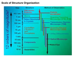
  • 1. Scale of Structure Organization
  • 3. Basics of Diffraction For electromagnetic radiation to be diffracted the spacing in the grating should be of the same order as the wavelength  In crystals the typical interatomic spacing ~ 2-3 Å so the suitable radiation is X-rays  Hence, X-rays can be used for the study of crystal structures  Neutrons and Electrons are also used for diffraction studies from materials.  Neutron diffraction is especially useful for studying the magnetic ordering in materials
  • 4.
  • 5.
  • 6.  The three X-ray scattering patterns above were produced by three chemically identical forms SiO2  Crystalline materials like quartz and Cristobalite produce X-ray diffraction patterns – Quartz and Cristobalite have two different crystal structures –The Si and O atoms are arranged differently, but both have long-range atomic order –The difference in their crystal structure is reflected in their different diffraction patterns  The amorphous glass does not have long-range atomic order and therefore produces only broad scattering features
  • 7.
  • 8.
  • 9. Optical Microscope Optical microscope is a type of microscope which uses visible light and a system of lenses to magnify images of small samples. There are two basic configurations of the conventional optical microscope in use, the simple (one lens) and the compound (many lenses).
  • 10. Assumptions in Light Theory 1.Light travels in a straight line. 2.Portions of light beams can be treated as individual rays. 3.Law of reflection. 4.Law of refraction.
  • 11. Simple Lens Kirkpatrick/Francis – “Physics; A World View SPHERICAL SURFACE
  • 12. Optics of a Microscope Slide with the letter “F” The letter “F” as it appears when viewed through the eyepiece F Images viewed through the eyepiece of compound microscopes will appear upside-down and backwards.
  • 13. How it Works? Light source or Mirror Optical Condenser Light passes through the specimen Objective Lenses (X100) First Image Eyepiece or Ocular (X10) Image (X1000) Retina
  • 14. Basic Components  Eyepiece Lens: the lens at the top that you look through.  Tube: Connects the eyepiece to the objective lenses  Objective Lenses: Usually you will find 3 or 4 objective lenses on a microscope. They almost always consist of 5X, 10X, 20X , 50X and 100X powers.  Rack Stop: This is an adjustment that determines how close the objective lens can get to the slide.  Condenser Lens: The purpose of the condenser lens is to focus the light onto the specimen.
  • 15. Basic Components  Stage: The flat platform where you place your slides. Stage clips hold the slides in place.  Revolving Nosepiece or Turret: This is the part that holds two or more objective lenses and can be rotated to easily change power.  Illuminator: A steady light source (110 volts) used in place of a mirror. If your microscope has a mirror, it is used to reflect light from an external light source.  Arm: Supports the tube and connects it to the base  Base: The bottom of the microscope, used for support
  • 16. Total Magnification • The total magnification of the specimen being viewed is calculated using the ocular lens multiplied by the objective lens. • For example, if the ocular lens is 10x and the ocular lens is 50x then the total magnification would be 500x.
  • 18. Focusing a Microscope • Course-adjustment knob- is the larger of the two knobs. It is used in bringing the object into quick focus. • Fine-adjustment knob- is used for improving the clarity of the image, especially when viewing under high power.
  • 19. Quality of an Image • Focal Length • Size of sample • Type of sample • Quality of Microscope and lenses • Amount of light on the sample • Quality of sample
  • 20. Numerical Aperture (NA) The objective collects as much light as possible coming from any point on the specimen and combines this light to form the image. The numerical aperture (NA) is a measure of the light collection capability of the objective and is defined as 𝑵𝑨 = 𝒏. 𝐬𝐢𝐧 𝜶 Objectives with a shorter focal length have a wider angular aperture and therefore deliver a higher NA and resolution.
  • 21. Numerical Aperture (NA) The objective with the higher numerical aperture is clearly able to give us more detail with separation between the wavelets. https://microscopeclarity.com/what-is-microscope-resolution/
  • 22. Depth of Field • The depth of field is the distance along the optical axis over which details of the object can be observed with adequate sharpness • "Depth of field" refers to the thickness of the plane of focus. • It is the vertical distance (from above to below the focal plane) that yields a useful image.
  • 23. The series of images show how the depth of field can influence the appearance of an image. With narrow depth of field, only part of the image is in focus at the same time. With a large depth of field, the entire image is in focus at the same time. Depth of Field: Example
  • 24. Resolution • Resolution or resolving power is the closest spacing of two points which can clearly be seen through the microscope to be separate entities. • It is not necessarily the same as the smallest point which can be seen with the microscope, which will often be smaller than the resolution limit. • Resolving power, 𝑑 = 0.61𝜆 𝑛.sin 𝛼 = 0.61𝜆 𝑁𝐴
  • 26. • Inexpensive • Easy to learn and operate • Very sharp plane of focus • Small and portable Advantages • Magnification is limited • Specimen may be disfigured during preparation to be viewed under the microscope. • Only has a resolution of 0.2 μm - which is relatively poor in comparison to other microscopes. • Poor surface view Disadvantages
  • 27. Allotriomorphic ferrite in a Fe-0.4C steel which is slowly cooled; the remaining dark-etching microstructure is fine pearlite Optical micrograph showing colonies of pearlite (courtesy S. S. Babu) https://www.phase-trans.msm.cam.ac.uk/2008/Steel_Microstructure/SM.html Microstructure: Examples
  • 28. Left, as-cast cadmium etched with 2% nital, 30 x ; right, as-cast alloy of Cd and 10% Bi etched with 2% nital, 60 x . Microstructure: Examples
  • 29. Microstructure: Examples Superpure aluminum anodized using the method of Hone and Pearson (Ref. 56), polarized light, 32 x . Left, held 6 min at 375°C, partly recrystallized. Right, held 2 h at 375°C, fully recrystallized. (Courtesy of E. C. Pearson, Alcan International Ltd.)
  • 30. Color etching of various grain or mixed-crystal areas and sulphate layers of different thicknesses Ferrite-perlite microstructure, the ferrite is tinted while Fe3C is kept white Klemm (K) etch This contrasting visualizes the quality of a soft annealing (K) https://www.leica-microsystems.com/science-lab/metallography-with-color-and-contrast/ Microstructure: Examples
  • 31. Brightfield image of a cast austenite structure caused by a laser melting process Improved contrast using interference Microstructure: Examples The same sample in interference contrast showing clear contrasting of the dendrites (B) Klemm (K) etchant: 50 mL saturated aqueous sodium thiosulfate, 1 g potassium metabisulfites Beraha (B) etchant: (a) Stock solution: 1:2, 1:1, or 1:0.5 HCI-water (b) 100 mL stock solution plus 0.6-1.0 g potassium metabisulfite https://www.leica-microsystems.com/science-lab/metallography-with-color-and-contrast/
  • 33. Construction of SEM SEM Magnification range 15x to 200,000x Resolution of 50 Å Excellent depth of focus Relatively easy sample preparation
  • 34. A brief description of each system follows: 1. Vacuum system. A vacuum is required when using an electron beam because electrons will quickly disperse or scatter due to collisions with other molecules. 2. Electron beam generation system. This system is found at the top of the microscope column. This system generates the "illuminating" beam of electrons known as the primary electron beam. 3. Electron beam manipulation system. This system consists of electromagnetic lenses and coils located in the microscope column and control the size, shape, and position of the electron beam on the specimen surface. 4. Beam specimen interaction system. This system involves the interaction of the electron beam with the specimen and the types of signals that can be detected. 5. Detection system. This system can consist of several different detectors, each sensitive to different energy / particle emissions that occur on the sample. 6. Signal processing system. This system is an electronic system that processes the signal generated by the detection system and allows additional electronic manipulation of the image. 7. Display and recording system. This system allows visualization of an electronic signal using a cathode ray tube and permits recording of the results using photographic or magnetic media. Components of SEM
  • 35. Principle of SEM image formation When an electron beam is incident on the sample then many different types of signals are generated which are eventually used to observe or analyze morphology/ topology of the sample. SEM is also used for elemental and state analysis. These signals includes – Secondary electrons, Backscattered electrons, Auger electrons, Cathodoluminescence and X-rays. Interaction of Electrons with Specimen: Electrons entering specimen gets scattered within it and lose their energy gradually upon getting absorbed within the sample. Scattering range within specimen depends upon- Energy of electrons – More Energy More Scattering. Element’s atomic number (Z) making the sample - More Z Less Scattering. Density of constituent atoms – More Density less scattering.
  • 36. SEM Sample- Conducting samples provide a path to ground for the beam electrons, and therefore require no special preparation. Insulating materials, however, require a thin coating of a conductor (often carbon or gold) in order to prevent charging. Sample Preparation- It is done in order to eliminate the sample charging few steps are followed: 1. Charging: A thin metal coating of about 10nm is done on the sample because metal film is highly stable and its secondary electron yield is higher. Too thin coating is not preferred because continuity is lost. 2. Low accelerating voltage: Low KV value of about 1KV can be used to scan insulating samples because the number of incident electrons becomes equal to the number of emitted secondary electrons, implying that the sample is not charged. 3. Tilt Observation: In this case secondary electrons yield is higher as electron beam is entering at an angle. 4. Low Vacuum SEM observation: Ondecreasing the vacuum, the gas molecules within the sample chamberincreases, which get ionized due to electrons and thus, on reaching the specimen as positive ions neutralize the charging. SEM sample Preparation
  • 37.
  • 39. Construction of TEM Instrument components  Electron gun (described previously)  Condenser system (lenses & apertures for controlling illumination on specimen)  Specimen chamber assembly  Objective lens system (image-forming lens - limits resolution; aperture - controls imaging conditions)  Projector lens system (magnifies image or diffraction pattern onto final screen)