
Recommended
Recommended
More Related Content
What's hot
What's hot (20)
Similar to Original N-Channel Mosfet 2SK3047 K3047 3047 2A 800V TO-220F New Panasonic
Similar to Original N-Channel Mosfet 2SK3047 K3047 3047 2A 800V TO-220F New Panasonic (20)
More from AUTHELECTRONIC
More from AUTHELECTRONIC (20)
Recently uploaded
Recently uploaded (20)
Original N-Channel Mosfet 2SK3047 K3047 3047 2A 800V TO-220F New Panasonic
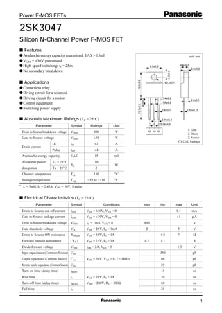
- 1. 1 Power F-MOS FETs unit: mm 2SK3047 Silicon N-Channel Power F-MOS FET s Features q Avalanche energy capacity guaranteed: EAS > 15mJ q VGSS = ±30V guaranteed q High-speed switching: tf = 25ns q No secondary breakdown s Applications q Contactless relay q Diving circuit for a solenoid q Driving circuit for a motor q Control equipment q Switching power supply s Electrical Characteristics (TC = 25°C) Parameter Drain to Source cut-off current Gate to Source leakage current Drain to Source breakdown voltage Gate threshold voltage Drain to Source ON-resistance Forward transfer admittance Diode forward voltage Input capacitance (Common Source) Output capacitance (Common Source) Reverse transfer capacitance (Common Source) Turn-on time (delay time) Rise time Turn-off time (delay time) Fall time Symbol IDSS IGSS VDSS Vth RDS(on) | Yfs | VDSF Ciss Coss Crss td(on) tr td(off) tf Conditions VDS = 640V, VGS = 0 VGS = ±30V, VDS = 0 ID = 1mA, VGS = 0 VDS = 25V, ID = 1mA VGS = 10V, ID = 1A VDS = 25V, ID = 1A IDR = 2A, VGS = 0 VDS = 20V, VGS = 0, f = 1MHz VGS = 10V, ID = 1A VDD = 200V, RL = 200Ω min 800 2 0.7 typ 4.8 1.1 350 60 25 15 20 60 25 max 0.1 ±1 5 7 −1.3 Unit mA µA V V Ω S V pF pF pF ns ns ns ns s Absolute Maximum Ratings (TC = 25°C) Parameter Drain to Source breakdown voltage Gate to Source voltage Drain current Avalanche energy capacity Allowable power dissipation Channel temperature Storage temperature DC Pulse TC = 25°C Ta = 25°C Symbol VDSS VGSS ID IDP EAS* PD Tch Tstg Ratings 800 ±30 ±2 ±4 15 30 2 150 −55 to +150 Unit V V A A mJ W °C °C * L = 5mH, IL = 2.45A, VDD = 50V, 1 pulse 1 9.9±0.3 15.0±0.513.7±0.2 4.2±0.2 4.6±0.2 2.9±0.2 0.8±0.1 1.4±0.2 2 3 φ3.2±0.1 2.6±0.1 0.55±0.15 2.54±0.3 5.08±0.5 3.0±0.5 1.6±0.2 1: Gate 2: Drain 3: Source TO-220D Package
- 2. 2 Power F-MOS FETs 2SK3047 Area of safe operation (ASO) PD Ta EAS Tj ID VDS ID VGS Vth TC RDS(on) ID | Yfs | ID Ciss, Coss, Crss VDS 1 10 100 10003 30 300 0.01 0.03 0.1 0.3 1 3 10 30 100 Non repetitive pulse TC=25˚C t =10µs 100µs DC 1ms 10ms 100ms Drain to source voltage VDS (V) DraincurrentID (A) 0 16040 12080 14020 10060 0 60 50 40 30 20 10 (1) TC=Ta (2) Without heat sink (1) (2) Ambient temperature Ta (˚C) AllowablepowerdissipationPD (W) 25 50 75 100 125 150 175 0 5 10 15 20 25 30 VDD=50V ID=2A Junction temperature Tj (˚C) AvalancheenergycapacityEAS(mJ) 0 10 20 30 40 50 60 0 1 2 3 4 VGS=15V 10V 6V 7V 5.5V 6.5V 5V TC=25˚C Drain to source voltage VDS (V) DraincurrentID (A) 0 121082 64 0 1 2 3 4 5 TC=0˚C 25˚C 100˚C 125˚C VDS=25V Gate to source voltage VGS (V) DraincurrentID (A) 0 25 50 75 100 125 150 0 1 2 3 4 5 6 VDS=25V ID=1mA Case temperature TC (˚C) GatethresholdvoltageVth (V) 0 1 2 3 4 5 0 12 10 8 6 4 2 VGS=10V 15V Drain current ID (A) DraintosourceON-resistanceRDS(on) (Ω) 30 1 2 4 0 0.5 1.0 1.5 2.0 VDS=25V TC=25˚C Drain current ID (A) Forwardtransferadmittance|Yfs|(S) 0 50 100 150 200 1 10 100 1000 10000 Ciss Coss Crss f=1MHz TC=25˚C Drain to source voltage VDS (V) Inputcapacitance(Commonsource),Outputcapacitance(Commonsource), Reversetransfercapacitance(Commonsource)Ciss,Coss,Crss (pF)
- 3. 3 Power F-MOS FETs 2SK3047 VDS, VGS Qg td(on), tr, tf, td(off) ID Rth(t) t 10–4 1010–3 10–110–2 1 103102 104 10–2 10–1 1 10 102 (1) Without heat sink (2) With a 100 × 100 × 2mm Al heat sink (1) (2) Time t (s) ThermalresistanceRth(t)(˚C/W) 0 4 8 12 16 20 24 0 100 200 300 400 500 600 700 800 0 4 8 12 16 2 6 10 14 VGSVDS ID=2A TC=25˚C GatetosourcevoltageVGS (V) Gate charge amount Qg (nC) DraintosourcevoltageVDS (V) 0 0.5 1.0 1.5 2.0 2.5 0 20 40 60 80 100 120 td(off) tf tr td(on) VDD=200V VGS=10V TC=25˚C Drain current ID (A) Switchingtimetd(on),tr,tf,td(off) (ns)