
Recommended
More Related Content
What's hot
What's hot (10)
Similar to Original N-Channel Mosfet IC 20N15GH 20N15 TO-252 New Advanced Power Electronics Corp.
Similar to Original N-Channel Mosfet IC 20N15GH 20N15 TO-252 New Advanced Power Electronics Corp. (20)
More from AUTHELECTRONIC
More from AUTHELECTRONIC (20)
Recently uploaded
Recently uploaded (20)
Original N-Channel Mosfet IC 20N15GH 20N15 TO-252 New Advanced Power Electronics Corp.
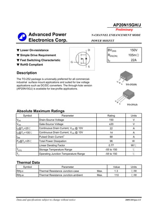
- 1. Advanced Power N-CHANNEL ENHANCEMENT MODE Electronics Corp. POWER MOSFET ▼▼▼▼ Lower On-resistance BVDSS 150V ▼▼▼▼ Simple Drive Requirement RDS(ON) 105mΩ ▼▼▼▼ Fast Switching Characteristic ID 22A ▼▼▼▼ RoHS Compliant Description Absolute Maximum Ratings Symbol Units VDS V VGS V ID@TC=25℃ A ID@TC=100℃ A IDM A PD@TC=25℃ W W/℃ TSTG ℃ TJ ℃ Symbol Value Units Rthj-c Thermal Resistance Junction-case Max. 1.3 ℃/W Rthj-a Thermal Resistance Junction-ambient Max. 110 ℃/W Data and specifications subject to change without notice Thermal Data Parameter 200913051pre-1/2 Pulsed Drain Current1 88 Operating Junction Temperature Range -55 to 150 Linear Derating Factor 0.77 Storage Temperature Range Total Power Dissipation 96 -55 to 150 Continuous Drain Current, VGS @ 10V 22 Continuous Drain Current, VGS @ 10V 14 Drain-Source Voltage 150 Gate-Source Voltage ±20 AP20N15GH/J Parameter Rating Preliminary G D S G D S TO-252(H) G D S TO-251(J) The TO-252 package is universally preferred for all commercial- industrial surface mount applications and suited for low voltage applications such as DC/DC converters. The through-hole version (AP20N15GJ) is available for low-profile applications.
- 2. Electrical Characteristics@Tj=25o C(unless otherwise specified) Symbol Parameter Test Conditions Min. Typ. Max. Units BVDSS Drain-Source Breakdown Voltage VGS=0V, ID=1mA 150 - - V ΔBVDSS/ΔTj Breakdown Voltage Temperature Coefficient Reference to 25℃, ID=1mA - 0.1 - V/℃ RDS(ON) Static Drain-Source On-Resistance2 VGS=10V, ID=14A - - 105 mΩ VGS(th) Gate Threshold Voltage VDS=VGS, ID=250uA 2 - 4 V gfs Forward Transconductance VDS=10V, ID=14A - 15 - S IDSS Drain-Source Leakage Current (Tj=25o C) VDS=150V, VGS=0V - - 25 uA Drain-Source Leakage Current (Tj=150o C) VDS=120V ,VGS=0V - - 100 uA IGSS Gate-Source Leakage VGS= ±20V - - ±100 nA Qg Total Gate Charge2 ID=14A - 18 28 nC Qgs Gate-Source Charge VDS=120V - 6 - nC Qgd Gate-Drain ("Miller") Charge VGS=10V - 5.7 - nC td(on) Turn-on Delay Time2 VDS=75V - 12 - ns tr Rise Time ID=14A - 30 - ns td(off) Turn-off Delay Time RG=10Ω,VGS=10V - 17 - ns tf Fall Time RD=5.4Ω - 2 - ns Ciss Input Capacitance VGS=0V - 1070 1720 pF Coss Output Capacitance VDS=25V - 240 - pF Crss Reverse Transfer Capacitance f=1.0MHz - 8 - pF Rg Gate Resistance f=1.0MHz - 1.5 2.3 Ω Source-Drain Diode Symbol Parameter Test Conditions Min. Typ. Max. Units VSD Forward On Voltage2 IS=14A, VGS=0V - - 1.3 V trr Reverse Recovery Time IS=14A, VGS=0V, - 130 - ns Qrr Reverse Recovery Charge dI/dt=100A/µs - 700 - nC Notes: 1.Pulse width limited by safe operating area. 2.Pulse width <300us , duty cycle <2%. 2/2 AP20N15GH/J