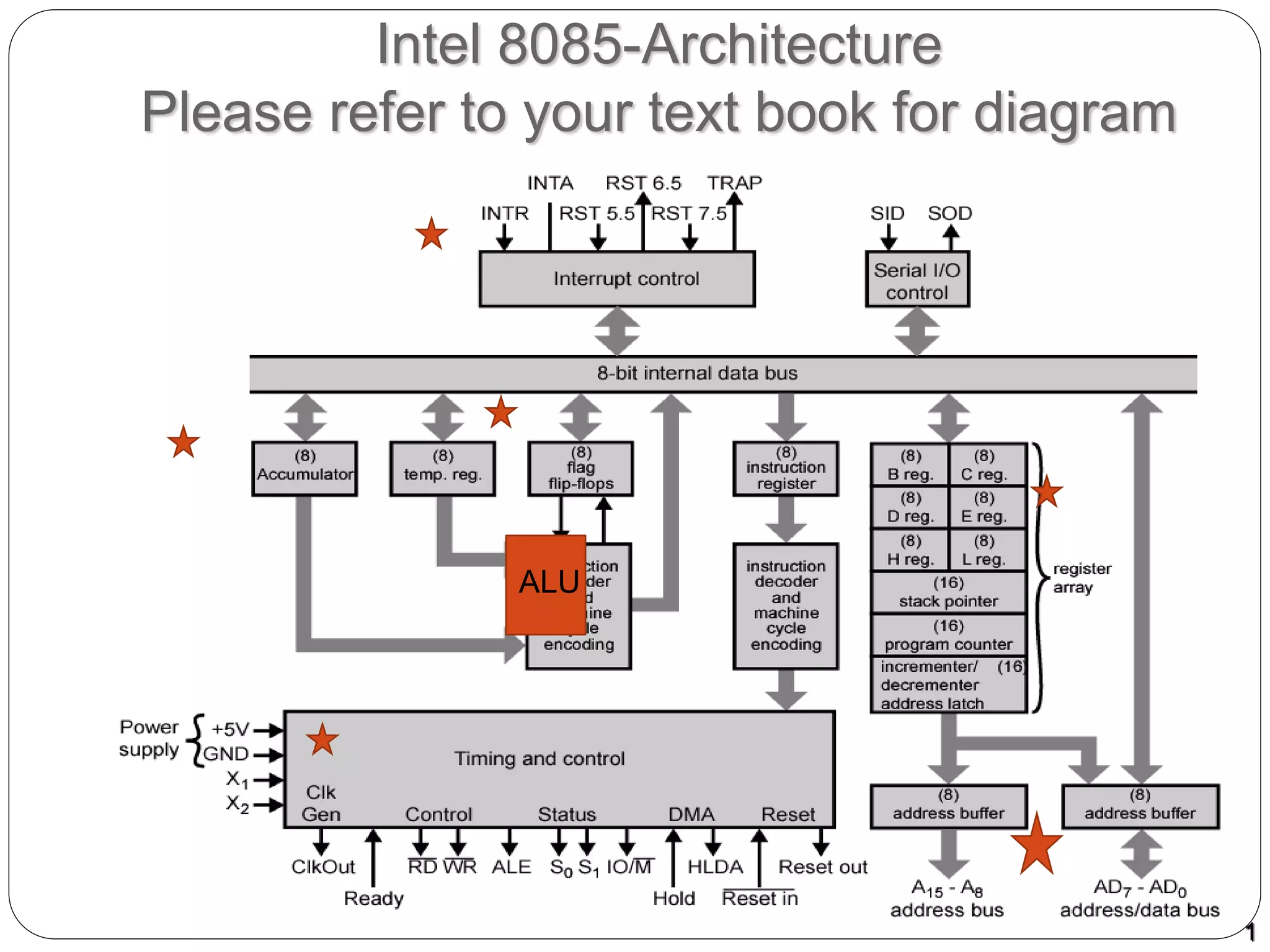
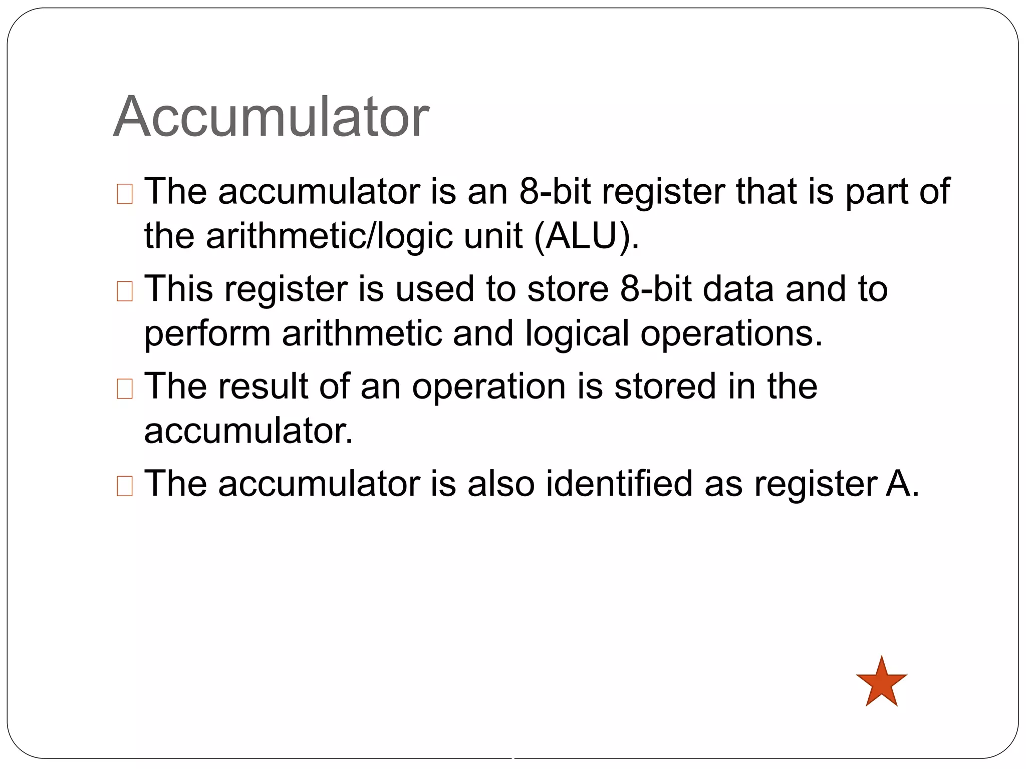
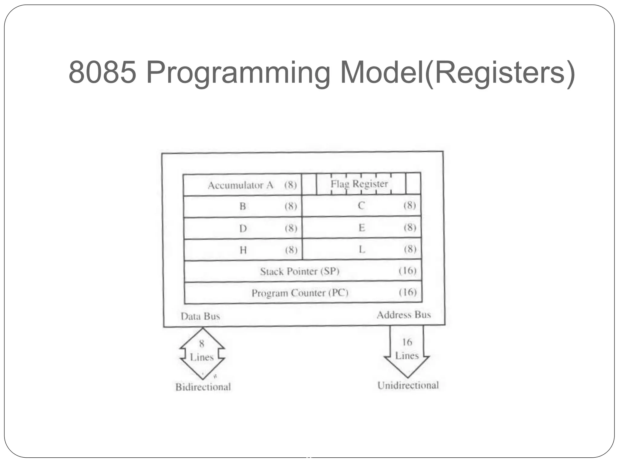
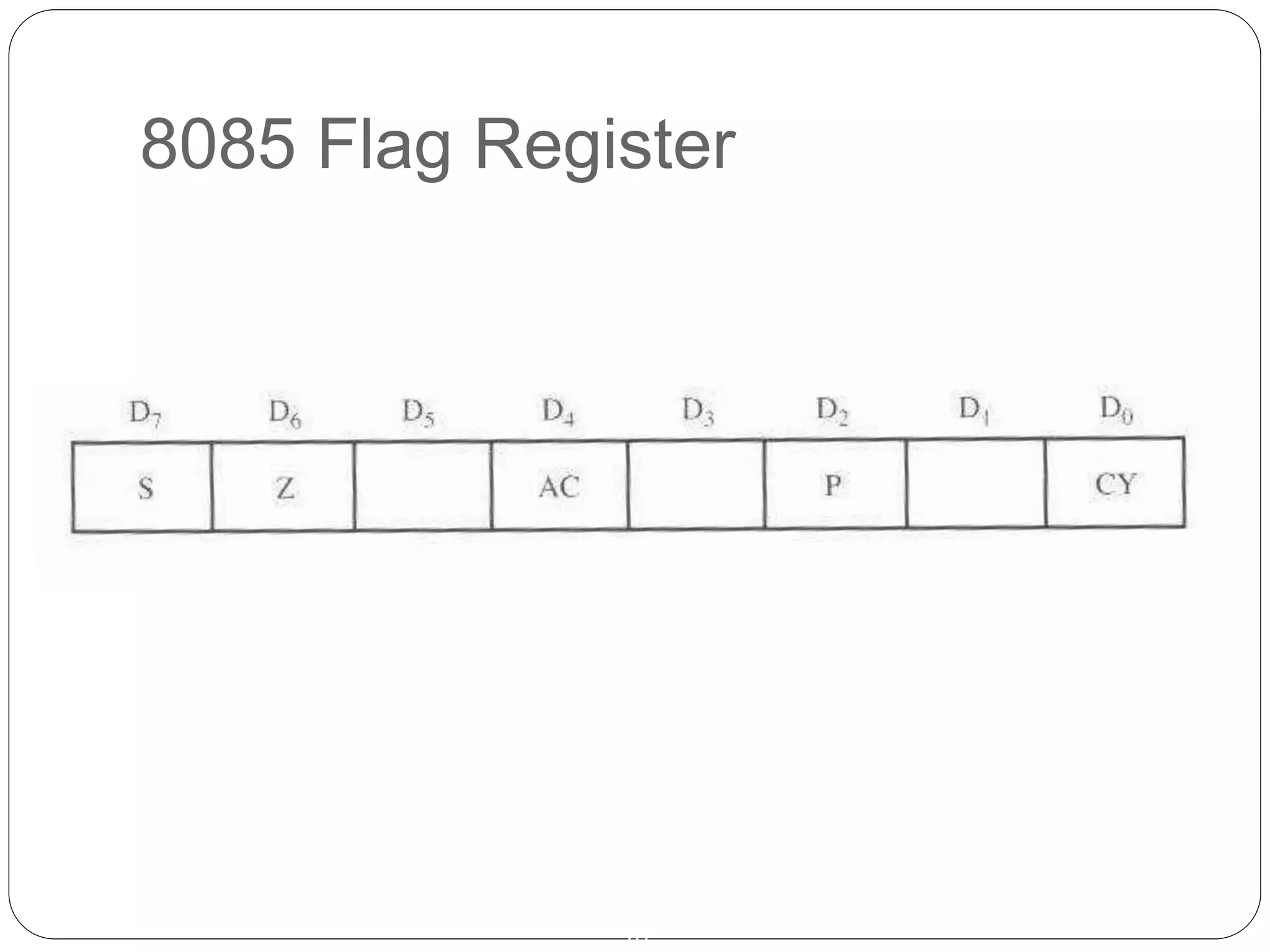
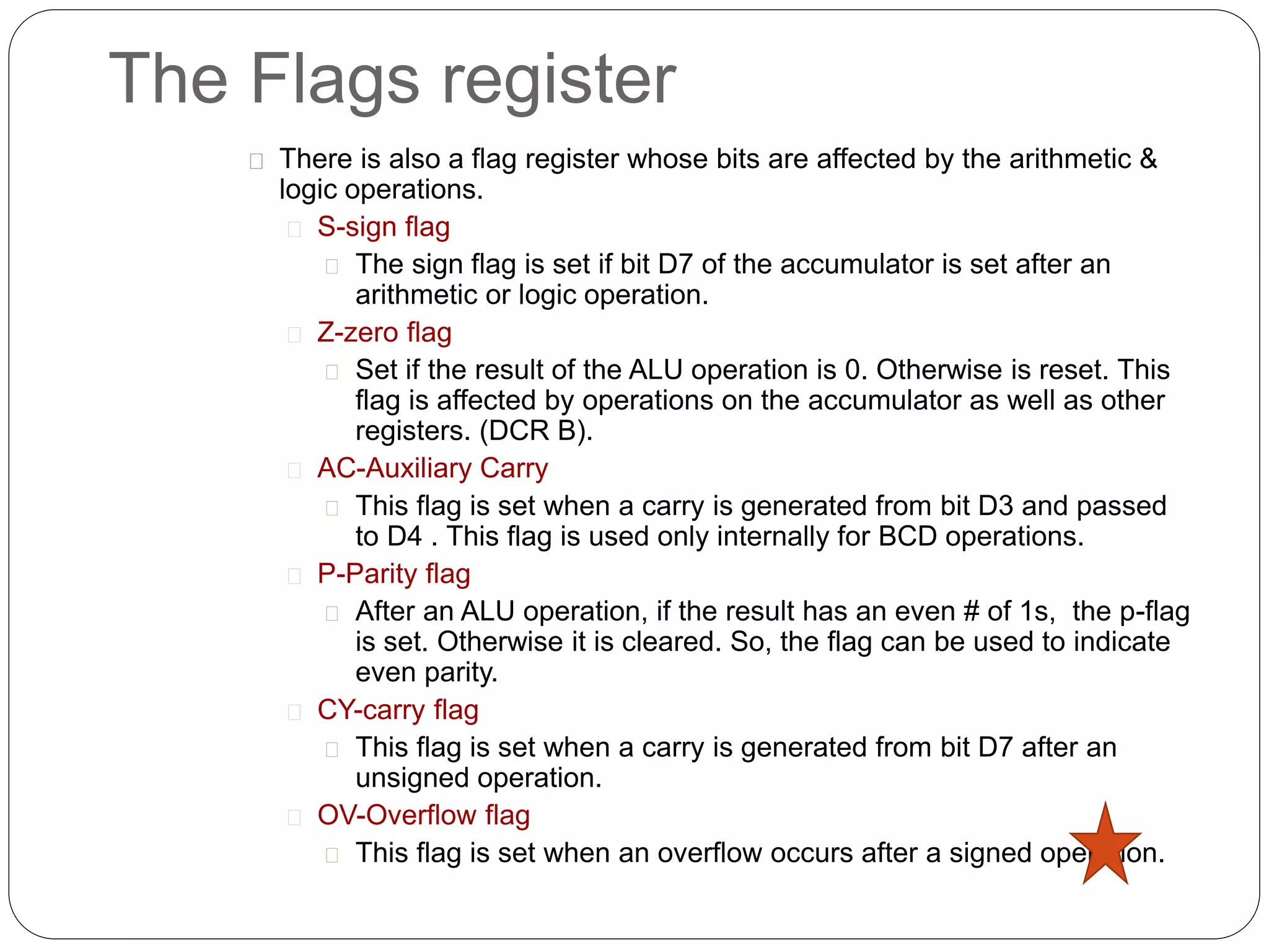
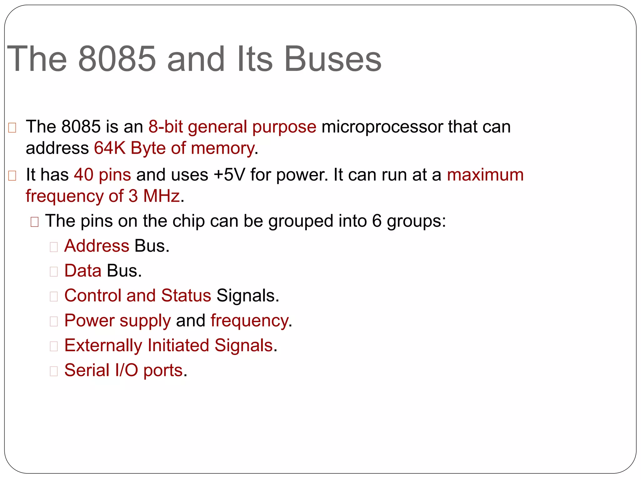
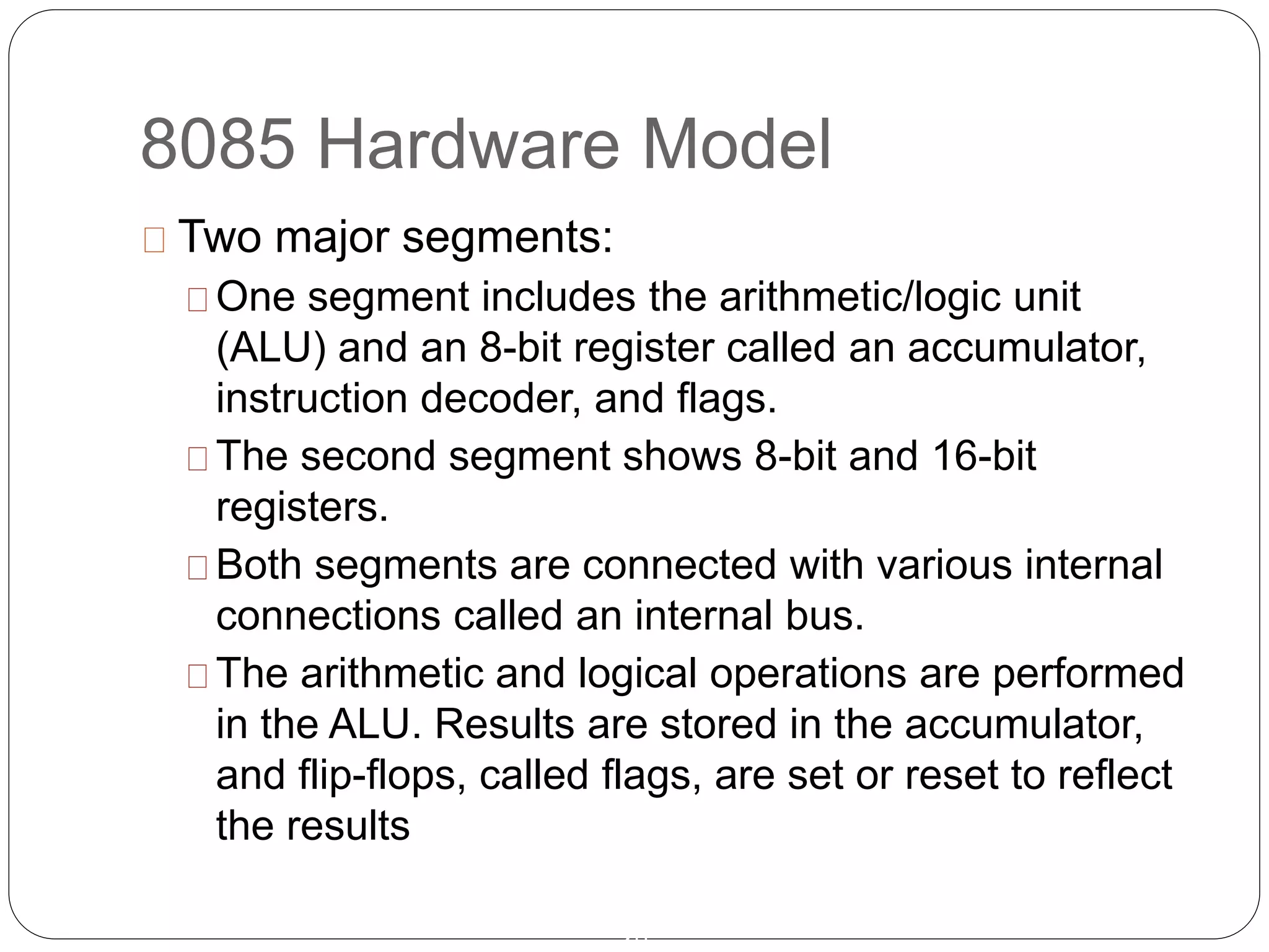
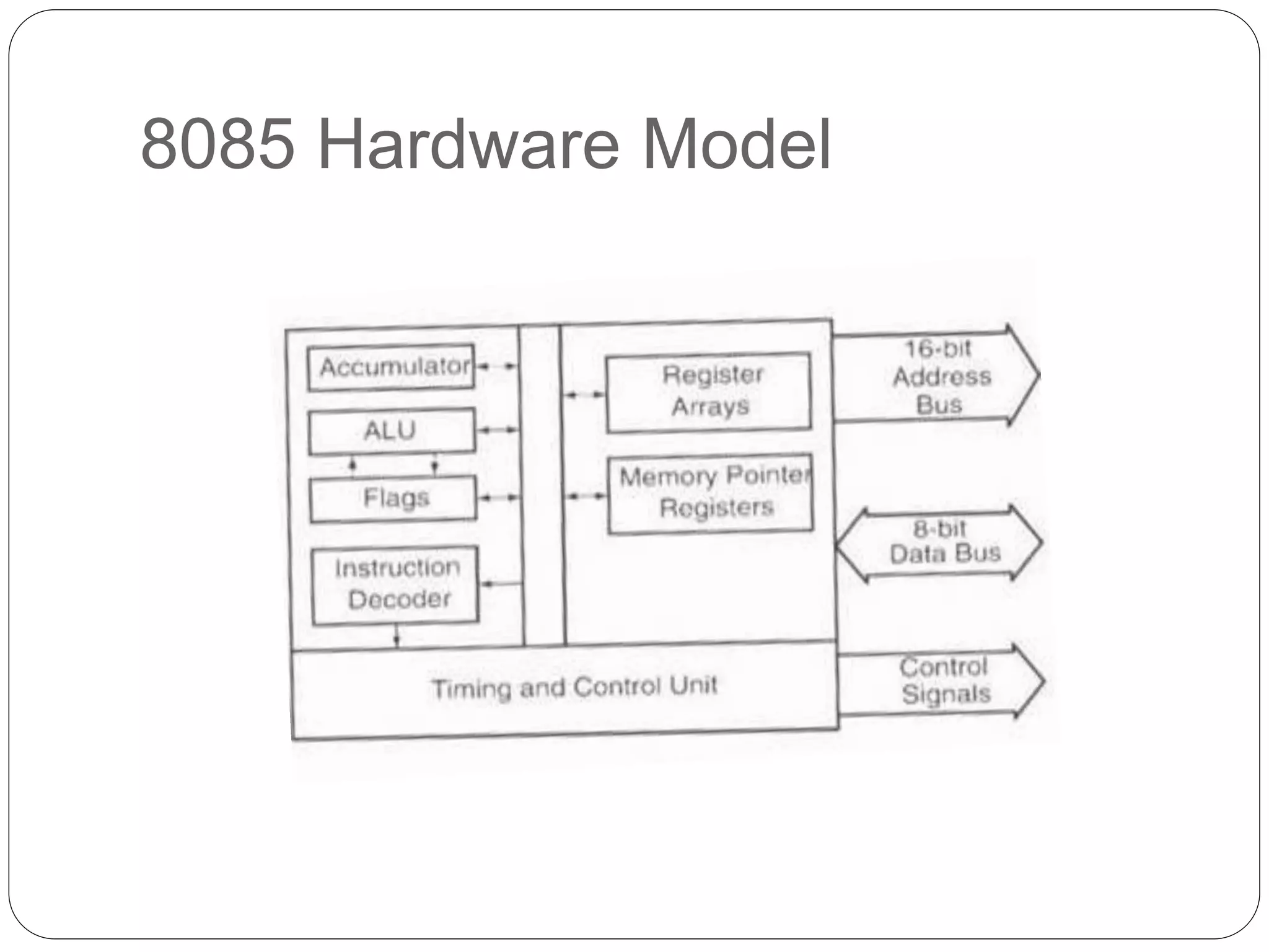
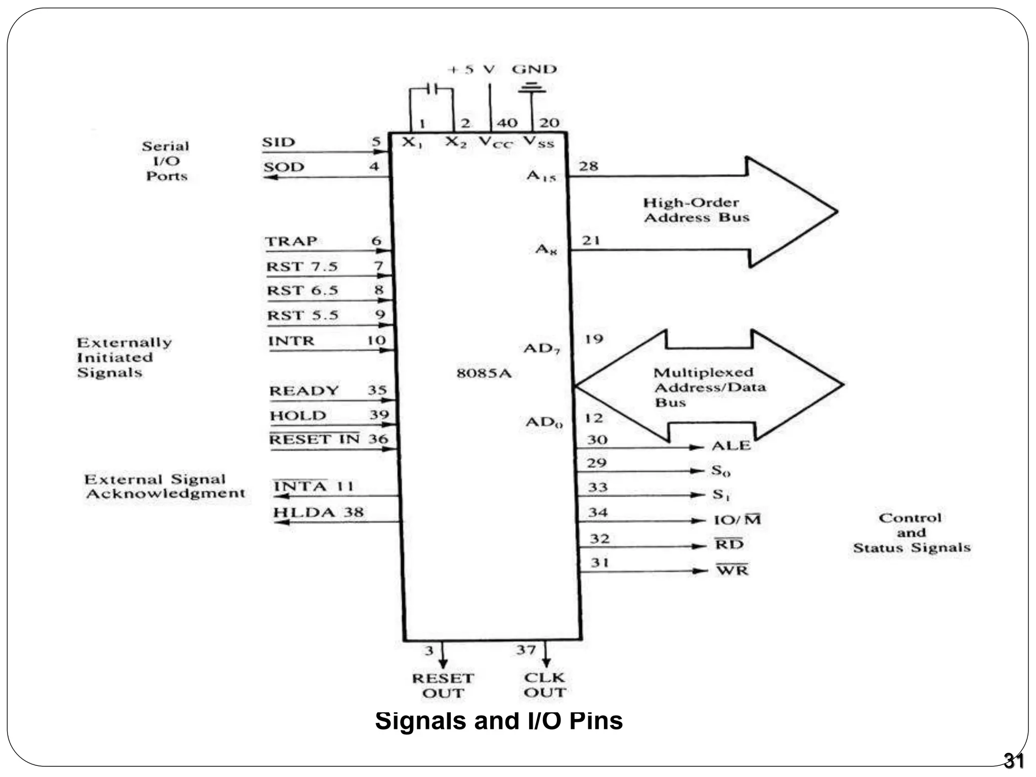
1
Intel 8085-Architecture
Please refer to your text book for diagram
ALU
Accumulator
2
The accumulator is an 8-bit register that is part of
the arithmetic/logic unit (ALU).
This register is used to store 8-bit data and to
perform arithmetic and logical operations.
The result of an operation is stored in the
accumulator.
The accumulator is also identified as register A.
8085 Programming Model(Registers)
3
The model includes six 8-bit registers (B, C, D, E,
H & L), one accumulator, and one flag register.
It also has two 16-bit registers:
the stack pointer (SP);
the program counter (PC).
8085 Programming Model(Registers)
4
General-purpose Registers
5
The 8085 has six general-purpose registers to
store 8-hit data;
B, C, D, E, H, and L.
They can be combined as register pairs - BC, DE,
and HL - to perform some 16-bit operations.
The programmer can use these registers to store
or copy data into the registers by using data copy
instructions.
Program COUNTER (PC) AND
STACK POINTER (SP)
6
These are two 16-bit registers used to hold
memory addresses.
PC:
The function of the PC is to point to the memory
address from which the next byte is to be fetched.
When a byte (machine code) is being fetched, the
program counter is incremented by one to point to
the next memory location.
Program COUNTER (PC) AND
STACK POINTER (SP)
7
SP:
It points to a memory location in R/W memory,
called the stack.
The beginning of the stack is defined by loading a
16-bit address in the stack pointer.
The PC will automatically update when calling to
/returning from Subroutines.
Stack
8
The stack is one of the most important things you
must know when programming.
Think of the stack as a deck of cards. When you put
a card on the deck, it will be the top card. Then you
put another card, then another.
When you remove the cards, you remove them
backwards, the last card first and so on.
The stack works the same way, you put (push)
words (addresses or register pairs) on the stack and
then remove (pop) them backwards.
That's called LIFO, Last In First Out.
Stack
9
There are instructions that allow you to modify SP
contents but you should NOT change the
contents of that register if you don't know what
you're doing!
PUSH
POP
8085 Flag Register
10
Flags
11
The ALU includes five flip-flops, which are set or
reset after an operation according to data
conditions of the result in the accumulator and
other registers.
They are called Zero (Z), Carry (CY), Sign (S),
Parity (P), and Auxiliary Carry (AC) flags;
The Flags register
There is also a flag register whose bits are affected by the arithmetic &
logic operations.
S-sign flag
The sign flag is set if bit D7 of the accumulator is set after an
arithmetic or logic operation.
Z-zero flag
Set if the result of the ALU operation is 0. Otherwise is reset. This
flag is affected by operations on the accumulator as well as other
registers. (DCR B).
AC-Auxiliary Carry
This flag is set when a carry is generated from bit D3 and passed
to D4 . This flag is used only internally for BCD operations.
P-Parity flag
After an ALU operation, if the result has an even # of 1s, the p-flag
is set. Otherwise it is cleared. So, the flag can be used to indicate
even parity.
CY-carry flag
This flag is set when a carry is generated from bit D7 after an
unsigned operation.
OV-Overflow flag
This flag is set when an overflow occurs after a signed operation.
8085 Hardware Model
13
There are three buses:
a 16-bit unidirectional address bus to send out
memory addresses;
an 8-bit bidirectional data bus, and a control bus to
transfer data, and.
the control bus for timing signals.
The 8085 and Its Buses
The 8085 is an 8-bit general purpose microprocessor that can
address 64K Byte of memory.
It has 40 pins and uses +5V for power. It can run at a maximum
frequency of 3 MHz.
The pins on the chip can be grouped into 6 groups:
Address Bus.
Data Bus.
Control and Status Signals.
Power supply and frequency.
Externally Initiated Signals.
Serial I/O ports.
ALE used to demultiplex address/data bus
The Address and Data Bus Systems
The address bus has 8 signal lines A8 – A15 which are
unidirectional.
The other 8 address bits are multiplexed (time shared) with the 8
data bits.
So, the bits AD0 – AD7 are bi-directional and serve as A0 – A7 and
D0 – D7 at the same time.
During the execution of the instruction, these lines carry the
address bits during the early part, then during the late parts of
the execution, they carry the 8 data bits.
In order to separate the address from the data, we can use a latch
to save the value before the function of the bits changes.
Address bus
The address bus is 'unidirectional', over which
the microprocessor sends an address code to
the memory or input/output.
The size (width) of the address bus is specified
by the number of bits it can handle.
The more bits there are in the address bus, the
more memory locations a microprocessor can
access.
A 16 bit address bus is capable of addressing
65,536 (64K) addresses.
Data bus
The data bus is 'bi-directional'
data or instruction codes from memory or
input/output.are transferred into the
microprocessor
the result of an operation or computation is sent
out from the microprocessor to the memory or
input/output.
Depending on the particular microprocessor,
the data bus can handle 8 bit or 16 bit data.
Control bus
The control bus is used by the microprocessor
to send out or receive timing and control signals
in order to coordinate and regulate its operation
and to communicate with other devices, i.e.
memory or input/output.
8085 Hardware Model
20
Two major segments:
One segment includes the arithmetic/logic unit
(ALU) and an 8-bit register called an accumulator,
instruction decoder, and flags.
The second segment shows 8-bit and 16-bit
registers.
Both segments are connected with various internal
connections called an internal bus.
The arithmetic and logical operations are performed
in the ALU. Results are stored in the accumulator,
and flip-flops, called flags, are set or reset to reflect
the results
8085 Hardware Model
21
BUS System
A15-A8
LatchAD7-AD0
D7- D0
A7- A0
8085
ALE
IO/MRDWR
1K Byte
Memory
Chip
WRRD
CS
A9- A0
A15- A10
Chip Selection
Circuit
8085 Pinout8085 μp consists of 16 signal pins use as address bus.
Divide into 2 part: A15 – A8 (upper) and
AD7 – AD0 (lower).
A15 – A8 : Unidirectional, known as ‘high order
address’.
AD7 – AD0 : bidirectional and dual purpose (address
and data placed once at a time).
AD7 – AD0 also known as ‘low order address’.
To execute an instruction, at early stage AD7 – AD0
uses as address bus and alternately as data bus for the
next cycle.
The method to change from address bus to data bus
known as ‘bus multiplexing’.
Control and Status Signals.
The Control and Status Signals
There are 4 main control and status signals. These are:
ALE: Address Latch Enable. This signal is a pulse that become
1 when the AD0 – AD7 lines have an address on them. It
becomes 0 after that. This signal can be used to enable a latch
to save the address bits from the AD lines.
RD: Read. Active low.
WR: Write. Active low.
IO/M: This signal specifies whether the operation is a memory
operation (IO/M=0) or an I/O operation (IO/M=1).
S1 and S0 : Status signals to specify the kind of operation
being performed. Usually not used in small systems.
Frequency Control Signals
There are 3 important pins in the frequency control group.
X0 and X1 are the inputs from the crystal or clock generating
circuit.
The frequency is internally divided by 2.
So, to run the microprocessor at 3 MHz, a clock running at 6
MHz should be connected to the X0 and X1 pins.
CLK (OUT): An output clock pin to drive the clock of the rest of the
system.
Clock Pins
8085 MPU has 3 pins
that control or present
the clock signal.
X1 and X2 pins
determine the clock
frequency.
CLK OUT is a TTL
square-wave output
clock.
The CLOCK OUT is
one-half the crystal
frequency.
8085A
X1 CLK OUT
X2
6 MHz
TRAP
RST7.5
RST6.5
RST 5.5
INTR
INTA
8085
8085 Interrupts
There are 5 interrupt inputs:
TRAP (nonmaskable)
RST7.5
RST6.5
RST5.5
INTR
8085 Interrupt Structure
Intel 8085 Pin
Configuration
31
Signals and I/O Pins

8085 architecture

  • 1.
    1 Intel 8085-Architecture Please referto your text book for diagram ALU
  • 2.
    Accumulator 2 The accumulator isan 8-bit register that is part of the arithmetic/logic unit (ALU). This register is used to store 8-bit data and to perform arithmetic and logical operations. The result of an operation is stored in the accumulator. The accumulator is also identified as register A.
  • 3.
    8085 Programming Model(Registers) 3 Themodel includes six 8-bit registers (B, C, D, E, H & L), one accumulator, and one flag register. It also has two 16-bit registers: the stack pointer (SP); the program counter (PC).
  • 4.
  • 5.
    General-purpose Registers 5 The 8085has six general-purpose registers to store 8-hit data; B, C, D, E, H, and L. They can be combined as register pairs - BC, DE, and HL - to perform some 16-bit operations. The programmer can use these registers to store or copy data into the registers by using data copy instructions.
  • 6.
    Program COUNTER (PC)AND STACK POINTER (SP) 6 These are two 16-bit registers used to hold memory addresses. PC: The function of the PC is to point to the memory address from which the next byte is to be fetched. When a byte (machine code) is being fetched, the program counter is incremented by one to point to the next memory location.
  • 7.
    Program COUNTER (PC)AND STACK POINTER (SP) 7 SP: It points to a memory location in R/W memory, called the stack. The beginning of the stack is defined by loading a 16-bit address in the stack pointer. The PC will automatically update when calling to /returning from Subroutines.
  • 8.
    Stack 8 The stack isone of the most important things you must know when programming. Think of the stack as a deck of cards. When you put a card on the deck, it will be the top card. Then you put another card, then another. When you remove the cards, you remove them backwards, the last card first and so on. The stack works the same way, you put (push) words (addresses or register pairs) on the stack and then remove (pop) them backwards. That's called LIFO, Last In First Out.
  • 9.
    Stack 9 There are instructionsthat allow you to modify SP contents but you should NOT change the contents of that register if you don't know what you're doing! PUSH POP
  • 10.
  • 11.
    Flags 11 The ALU includesfive flip-flops, which are set or reset after an operation according to data conditions of the result in the accumulator and other registers. They are called Zero (Z), Carry (CY), Sign (S), Parity (P), and Auxiliary Carry (AC) flags;
  • 12.
    The Flags register Thereis also a flag register whose bits are affected by the arithmetic & logic operations. S-sign flag The sign flag is set if bit D7 of the accumulator is set after an arithmetic or logic operation. Z-zero flag Set if the result of the ALU operation is 0. Otherwise is reset. This flag is affected by operations on the accumulator as well as other registers. (DCR B). AC-Auxiliary Carry This flag is set when a carry is generated from bit D3 and passed to D4 . This flag is used only internally for BCD operations. P-Parity flag After an ALU operation, if the result has an even # of 1s, the p-flag is set. Otherwise it is cleared. So, the flag can be used to indicate even parity. CY-carry flag This flag is set when a carry is generated from bit D7 after an unsigned operation. OV-Overflow flag This flag is set when an overflow occurs after a signed operation.
  • 13.
    8085 Hardware Model 13 Thereare three buses: a 16-bit unidirectional address bus to send out memory addresses; an 8-bit bidirectional data bus, and a control bus to transfer data, and. the control bus for timing signals.
  • 14.
    The 8085 andIts Buses The 8085 is an 8-bit general purpose microprocessor that can address 64K Byte of memory. It has 40 pins and uses +5V for power. It can run at a maximum frequency of 3 MHz. The pins on the chip can be grouped into 6 groups: Address Bus. Data Bus. Control and Status Signals. Power supply and frequency. Externally Initiated Signals. Serial I/O ports.
  • 15.
    ALE used todemultiplex address/data bus
  • 16.
    The Address andData Bus Systems The address bus has 8 signal lines A8 – A15 which are unidirectional. The other 8 address bits are multiplexed (time shared) with the 8 data bits. So, the bits AD0 – AD7 are bi-directional and serve as A0 – A7 and D0 – D7 at the same time. During the execution of the instruction, these lines carry the address bits during the early part, then during the late parts of the execution, they carry the 8 data bits. In order to separate the address from the data, we can use a latch to save the value before the function of the bits changes.
  • 17.
    Address bus The addressbus is 'unidirectional', over which the microprocessor sends an address code to the memory or input/output. The size (width) of the address bus is specified by the number of bits it can handle. The more bits there are in the address bus, the more memory locations a microprocessor can access. A 16 bit address bus is capable of addressing 65,536 (64K) addresses.
  • 18.
    Data bus The databus is 'bi-directional' data or instruction codes from memory or input/output.are transferred into the microprocessor the result of an operation or computation is sent out from the microprocessor to the memory or input/output. Depending on the particular microprocessor, the data bus can handle 8 bit or 16 bit data.
  • 19.
    Control bus The controlbus is used by the microprocessor to send out or receive timing and control signals in order to coordinate and regulate its operation and to communicate with other devices, i.e. memory or input/output.
  • 20.
    8085 Hardware Model 20 Twomajor segments: One segment includes the arithmetic/logic unit (ALU) and an 8-bit register called an accumulator, instruction decoder, and flags. The second segment shows 8-bit and 16-bit registers. Both segments are connected with various internal connections called an internal bus. The arithmetic and logical operations are performed in the ALU. Results are stored in the accumulator, and flip-flops, called flags, are set or reset to reflect the results
  • 21.
  • 22.
    BUS System A15-A8 LatchAD7-AD0 D7- D0 A7-A0 8085 ALE IO/MRDWR 1K Byte Memory Chip WRRD CS A9- A0 A15- A10 Chip Selection Circuit
  • 23.
    8085 Pinout8085 μpconsists of 16 signal pins use as address bus. Divide into 2 part: A15 – A8 (upper) and AD7 – AD0 (lower). A15 – A8 : Unidirectional, known as ‘high order address’. AD7 – AD0 : bidirectional and dual purpose (address and data placed once at a time). AD7 – AD0 also known as ‘low order address’. To execute an instruction, at early stage AD7 – AD0 uses as address bus and alternately as data bus for the next cycle. The method to change from address bus to data bus known as ‘bus multiplexing’.
  • 24.
  • 25.
    The Control andStatus Signals There are 4 main control and status signals. These are: ALE: Address Latch Enable. This signal is a pulse that become 1 when the AD0 – AD7 lines have an address on them. It becomes 0 after that. This signal can be used to enable a latch to save the address bits from the AD lines. RD: Read. Active low. WR: Write. Active low. IO/M: This signal specifies whether the operation is a memory operation (IO/M=0) or an I/O operation (IO/M=1). S1 and S0 : Status signals to specify the kind of operation being performed. Usually not used in small systems.
  • 26.
    Frequency Control Signals Thereare 3 important pins in the frequency control group. X0 and X1 are the inputs from the crystal or clock generating circuit. The frequency is internally divided by 2. So, to run the microprocessor at 3 MHz, a clock running at 6 MHz should be connected to the X0 and X1 pins. CLK (OUT): An output clock pin to drive the clock of the rest of the system.
  • 27.
    Clock Pins 8085 MPUhas 3 pins that control or present the clock signal. X1 and X2 pins determine the clock frequency. CLK OUT is a TTL square-wave output clock. The CLOCK OUT is one-half the crystal frequency. 8085A X1 CLK OUT X2 6 MHz
  • 28.
  • 29.
    There are 5interrupt inputs: TRAP (nonmaskable) RST7.5 RST6.5 RST5.5 INTR 8085 Interrupt Structure
  • 30.
  • 31.