SlideShare a Scribd company logo
1 of 35
1. Introduction 
Projet title is “Automatic Room Light Controller”. The objective of this project is 
to make a model to count number of person visiting particular room and accordingly 
light up the room. Here we can use sensonrs and can know present number of persons. 
In today’s world, there is a continuous need for automatic appliances with the 
increase in standard of living, there is a sense of urgency for developing circuits that 
would ease the complexity of life. 
Also if at all one wants to know the number of people present in room so as not 
to have congestion. This circuit proves to be helpful. The project is a reliable circuit 
that takes over the task of controlling the room lights as well as counting number of 
persons/visitors in the room very accurately. When somebody enters in the room then 
the counter is decremented by one. The light will be onlye switched OFF until all the 
persons in the room go out. The total number of persons inside the room is also 
displayed on the seven segment displays. 
The 555 timer does the above job.It receives the signals from the sensors, and this 
signal is operated under the control of software which is stored in 555 timer 
continuously monitor the Infrared Receivers. When any object pass through the IR’s 
Receivers then the IR rays falling on the receivers are obstructed, this obstraction is 
sensed by the 555 timer. 
2. Working Principle 
2.1 Circuit Diagram
There are two main part of the circuits. 
1. Transmission Circuit(Infrared Led’s) 
2. Receiver Circuit 
1. Transmission Circuit 
This circuit diagram show how a 555 timer IC, configured to function as a basic 
astable multivibrator. The astable multivibrator generates a square wave, the period of 
which is determined by the circuit external to IC 555. The astable multivibrator does 
not require any external trigger to change the state of the output. Hence the name free 
running oscillator. The time during which the output is either high or low is
determined by the two resistors and a capacitor which are externally connected to the 
555 timer. 
IR Transmission circuit is used to generate the modulated 36 kHz IR signal. The 
IC555 in the transmitter side is to generate 36 kHz square wave. Adjust the preset in 
the transmitter to get a 38 kHz signal at the output. Then you point it over the sensors 
and its output will go low when it senses the IR signal of 38 kHz. 
2. Receiver Circuit 
The IR transmitter will emit modulated 38 kHz IR signal and at the receiver we use 
TSPO1738(Infrared Sensor). The output goes high when there is an interruption and it 
return back to low after the time period determined by the capacitor and resistor in the 
circuit i.e. around 1 Second. CL100 is to trigger the IC555 which is configured as 
monostable multivibrator. Input is given to the port 1. Port 0 is user for the 7-Segment
display purpose. Port 2 is used for the relay Turn on and Turn off purpose. LTS 
542(Common Anode) is used for 7-Segment display and that time relay will get 
voltage and triggered, so light will get voltage and it will turn on and when counter 
will be 00 and at that time relay turned off. 
2.2 PCB Layout 
2.3 Components Lists 
2.4 Working 
This system is designed by using two sets of IR transmitters and receivers. These IR 
sensors are placed in such a way that they detect a person entering and leaving the 
room to turn the home appliances. In this optimum energy management system, a 
microcontroller is the central processing unit of this project which is of 89S51
controller from the 8051 family. This system facilitates a bidirectional visitor counter 
for displaying the number of persons inside the room. 
When a person enters into the room, an IR beam is obstructed between the IR 
transmitter and the receiver. This IR obstruction from the sensor-1 gives the 
corresponding signal to the microcontroller. The microcontroller in such a way that by 
the reception of the signal from the sensor-1 it turns on the fans and lights inside the 
room. Thus, the microcontroller gives command signals to a relay driver which turns 
the rellays such that all these appliances turn on. 
When the person leaves from this room, another set of IR sensors enable and give 
control signals to the microcontroller. Furthermore, similar to the above process, this 
system turns off the appliances like fans and lights. Apart from this, the system also 
takes account of the number of persons inside the room so that this control operation 
is varied depending on the persons’ availability in the room. 
For every person entering and leaving the room, the microcontroller reads the digital 
input from two receivers, and calculates the number of persons inside the room, and 
then displays it on the LCD. When the persons’ count is greater than one, the 
microcontroller turns on the room light and when the persons’ count is zero, it turns 
off all the lights and fans. 
3. DESIGN PROCEDURE 
3.1 Multivator 
A multivibrator circuit oscillates between a “HIGH” state and a “LOW” state 
producing a continuous output. Astable multivibrators generally have an even 50% 
duty cycle, that is that 50% of the cycle time the output is “HIGH” and the remaining 
50% of the cycle time the output is “OFF”. In other words, the duty cycle for an 
astable timing pulse is 1:1. 
Sequential Logic Circuits that use the clock signal for synchronization are dependant 
upon the frequency and and clock pulse width to activate there switching action. 
Sequential circuits may also change their state on either the rising or falling edge, or 
both of the actual clock signal as we have seen previously with the basic flip-flop 
circuits. The following list are terms associated with a timing pulse or waveform. 
Active HIGH - if the state change occurs from a “LOW” to a “HIGH” at the clock’s 
pulse rising edge or during the clock width.
Clock Signal Waveform 
Active LOW - if the state change occurs from a “HIGH” to a “LOW” at the clock’s 
pulses falling edge. 
Duty Cycle - this is the ratio of the clock width to the clock period. 
Clock Width - this is the time during which the value of the clock signal is equal to a 
logic “1”, or HIGH. 
Clock Period - this is the time between successive transitions in the same direction, 
ie, between two rising or two falling edges. 
Clock Frequency - the clock frequency is the reciprocal of the clock period, 
frequency = 1/clock period 
Clock pulse generation circuits can be a combination of analogue and digital circuits 
that produce a continuous series of pulses (these are called astable multivibrators) or a 
pulse of a specific duration (these are called monostable multivibrators). Combining 
two or more of multivibrators provides generation of a desired pattern of pulses 
(including pulse width, time between pulses and frequency of pulses). 
There are basically three types of clock pulse generation circuits: 
· Astable – A free-running multivibrator that has NO stable states but 
switches continuously between two states this action produces a train of square 
wave pulses at a fixed frequency. 
· Monostable – A one-shot multivibrator that has only ONE stable state and 
is triggered externally with it returning back to its first stable state. 
· Bistable – A flip-flop that has TWO stable states that produces a single 
pulse either positive or negative in value. 
One way of producing a very simple clock signal is by the interconnection of logic 
gates. As NANDgates contains amplification, they can also be used to provide a clock 
signal or timing pulse with the aid of a single Capacitor and a single Resistor to 
provide the feedback and timing function. 
These timing circuits are often used because of there simplicity and are also useful if a 
logic circuit is designed that has unused gates which can be utilised to create the 
monostable or astable oscillator. This simple type of RC Oscillator network is 
sometimes called a “Relaxation Oscillator”.
3.1 Operation: 
Figure 1: Basic BJT astable multivibrator 
The circuit has two astable (unstable) states that change alternatively with maximum 
transition rate because of the "accelerating" positive feedback. It is implemented by 
the coupling capacitors that instantly transfer voltage changes because the voltage 
across a capacitor cannot suddenly change. In each state, one transistor is switched on 
and the other is switched off. Accordingly, one fully charged capacitor discharges 
(reverse charges) slowly thus converting the time into an exponentially changing 
voltage. At the same time, the other empty capacitor quickly charges thus restoring its 
charge (the first capacitor acts as a time-setting capacitor and the second prepares to 
play this role in the next state). The circuit operation is based on the fact that the 
forward-biased base-emitter junction of the switched-on bipolar transistor can provide 
a path for the capacitor restoration. 
3.2 State 1 (Q1 is switched on, Q2 is switched off): 
In the beginning, the capacitor C1 is fully charged (in the previous State 2) to the 
power supply voltage V with the polarity shown in Figure 1. Q1 is on and connects 
the left-hand positive plate of C1 to ground. As its right-hand negative plate is 
connected to Q2 base, a maximum negative voltage (-V) is applied to Q2 base that 
keeps Q2 firmly off. C1 begins discharging (reverse charging) via the high-value base 
resistor R2, so that the voltage of its right-hand plate (and at the base of Q2) is rising 
from below ground (-V) toward +V. As Q2 base-emitter junction is backward-biased, 
it does not conduct, so all the current from R2 goes into C1. Simultaneously, C2 that 
is fully discharged and even slightly charged to 0.6 V (in the previous State 2) quickly 
charges via the low-value collector resistor R4 and Q1 forward-biased base-emitter 
junction (because R4 is less than R2, C2 charges faster than C1). Thus C2 restores its 
charge and prepares for the next State C2 when it will act as a time-setting capacitor. 
Q1 is firmly saturated in the beginning by the "forcing" C2 charging current added to 
R3 current; in the end, only R3 provides the needed input base current. The resistance 
R3 is chosen small enough to keep Q1 (not deeply) saturated after C2 is fully charged.
When the voltage of C1 right-hand plate (Q2 base voltage) becomes positive and 
reaches 0.6 V, Q2 base-emitter junction begins diverting a part of R2 charging current. 
Q2 begins conducting and this starts the avalanche-like positive feedback process as 
follows. Q2 collector voltage begins falling; this change transfers through the fully 
charged C2 to Q1 base and Q1 begins cutting off. Its collector voltage begins rising; 
this change transfers back through the almost empty C1 to Q2 base and makes Q2 
conduct more thus sustaining the initial input impact on Q2 base. Thus the initial 
input change circulates along the feedback loop and grows in an avalanche-like 
manner until finally Q1 switches off and Q2 switches on. The forward-biased Q2 
base-emitter junction fixes the voltage of C1 right-hand plate at 0.6 V and does not 
allow it to continue rising toward +V. 
3.3 State 2 (Q1 is switched off, Q2 is switched on): 
Now, the capacitor C2 is fully charged (in the previous State 1) to the power supply 
voltage V with the polarity shown in Figure 1. Q2 is on and connects the right-hand 
positive plate of C2 to ground. As its left-hand negative plate is connected to Q1 base, 
a maximum negative voltage (-V) is applied to Q1 base that keeps Q1 firmly off. C2 
begins discharging (reverse charging) via the high-value base resistor R3, so that the 
voltage of its left-hand plate (and at the base of Q1) is rising from below ground (-V) 
toward +V. Simultaneously, C1 that is fully discharged and even slightly charged to 
0.6 V (in the previous State 1) quickly charges via the low-value collector resistor R1 
and Q2 forward-biased base-emitter junction (because R1 is less than R3, C1 charges 
faster than C2). Thus C1 restores its charge and prepares for the next State 1 when it 
will act again as a time-setting capacitor...and so on... 
3.4 Multivibrator frequency 
Derivation 
The duration of state 1 (low output) will be related to the time constant R2C1 as it 
depends on the charging of C1, and the duration of state 2 (high output) will be 
related to the time constant R3C2 as it depends on the charging of C2. Because they do 
not need to be the same, an asymmetric duty cycle is easily achieved. 
The voltage on a capacitor with non-zero initial charge is: 
Looking at C2, just before Q2 turns on, the left terminal of C2 is at the base-emitter 
voltage of Q1 (VBE_Q1) and the right terminal is at VCC ("VCC" is used here
instead of "+V" to ease notation). The voltage across C2 is VCC minus VBE_Q1 . The 
moment after Q2 turns on, the right terminal of C2 is now at 0 V which drives the 
left terminal of C2 to 0 V minus (VCC - VBE_Q1) or VBE_Q1 - VCC. From this instant in 
time, the left terminal of C2 must be charged back up to VBE_Q1. How long this 
takes is half our multivibrator switching time (the other half comes from C1). In 
the charging capacitor equation above, substituting: 
VBE_Q1 for 
(VBE_Q1 - VCC) for 
VCC for 
results in: 
Solving for t results in: 
For this circuit to work, VCC>>VBE_Q1 (for example: VCC=5 V, 
VBE_Q1=0.6 V), therefore the equation can be simplified to: 
or 
or 
The period of each half of the multivibrator is therefore given by t = ln(2)RC. 
The total period of oscillation is given by: 
T = t1 + t2 = ln(2)R2 C1 + ln(2)R3 C2 
where...
· f is frequency in hertz. 
· R2 and R3 are resistor values in ohms. 
· C1 and C2 are capacitor values in farads. 
· T is the period (In this case, the sum of two period durations). 
For the special case where 
· t1 = t2 (50% duty cycle) 
· R2 = R3 
· C1 = C2 
3.5 Output pulse shape 
The output voltage has a shape that approximates a square waveform. It is considered 
below for the transistor Q1. 
During State 1, Q2 base-emitter junction is reverse-biased and the capacitor C1 is 
"unhooked" from ground. The output voltage of the switched-on transistor Q1 
changes rapidly from high to low since this low-resistive output is loaded by a high 
impedance load (the series connected capacitor C1 and the high-resistive base resistor 
R2). 
During State 2, Q2 base-emitter junction is forward-biased and the capacitor C1 is 
"hooked" to ground. The output voltage of the switched-off transistor Q1 changes 
exponentially from low to high since this relatively high resistive output is loaded by 
a low impedance load (the capacitance C1). This is the output voltage of 
R1C1 integrating circuit. 
To approach the needed square waveform, the collector resistors have to be low 
resistance. The base resistors have to be low enough to make the transistors saturate in 
the end of the restoration (RB < β.RC). 
3.6 Initial power-up: 
When the circuit is first powered up, neither transistor will be switched on. However, 
this means that at this stage they will both have high base voltages and therefore a 
tendency to switch on, and inevitable slight asymmetries will mean that one of the 
transistors is first to switch on. This will quickly put the circuit into one of the above 
states, and oscillation will ensue. In practice, oscillation always occurs for practical 
values of R and C.
However, if the circuit is temporarily held with both bases high, for longer than it 
takes for both capacitors to charge fully, then the circuit will remain in this stable 
state, with both bases at 0.6 V, both collectors at 0 V, and both capacitors charged 
backwards to −0.6 V. This can occur at startup without external intervention, 
if R and C are both very small. 
3.7 Frequency divider: 
An astable multivibrator can be synchronized to an external chain of pulses. A single 
pair of active devices can be used to divide a reference by a large ratio, however, the 
stability of the technique is poor owing to the variability of the power supply and the 
circuit elements; a division ratio of 10, for example, is easy to obtain but not 
dependable. Chains of bistable flip-flops provide more predictable division, at the cost 
of more active elements. 
3.8 Protective components: 
While not fundamental to circuit operation, diodes connected in series with the base 
or emitter of the transistors are required to prevent the base-emitter junction being 
driven into reverse breakdown when the supply voltage is in excess of 
the Veb breakdown voltage, typically around 5-10 volts for general purpose silicon 
transistors. In the monostable configuration, only one of the transistors requires 
protection. 
3.9 Astablemultivibrator: 
Astable Multivibrators are the most commonly used type of multivibrator 
circuit. An astable multivibrator is a free running oscillator that have no permanent 
“meta” or “steady” state but are continually changing there output from one state 
(LOW) to the other state (HIGH) and then back again. This continual switching action 
from “HIGH” to “LOW” and “LOW” to “HIGH” produces a continuous and stable 
square wave output that switches abruptly between the two logic levels making it 
ideal for timing and clock pulse applications. 
As with the previous monostable multivibrator circuit above, the timing cycle is 
determined by the RC time constant of the resistor-capacitor, RC Network. Then the 
output frequency can be varied by changing the value(s) of the resistors and capacitor 
in the circuit.
NAND Gate Astable Multivibrator 
The astable multivibrator circuit uses two CMOS NOT gates such as the CD4069 or 
the 74HC04 hex inverter ICs, or as in our simple circuit below a pair of 
CMOS NAND such as the CD4011 or the 74LS132 and an RC timing network. The 
two NAND gates are connected as inverting NOT gates. 
Suppose that initially the output from the NAND gate U2 is HIGH at logic level “1”, 
then the input must therefore be LOW at logic level “0” (NAND gate principles) as 
will be the output from the first NAND gate U1. Capacitor, C is connected between 
the output of the second NAND gate U2 and its input via the timing resistor, R2. The 
capacitor now charges up at a rate determined by the time constant of R2 and C. 
As the capacitor, C charges up, the junction between the resistor R2 and the 
capacitor, C, which is also connected to the input of the NAND gate U1 via the 
stabilizing resistor, R2 decreases until the lower threshold value of U1 is reached at 
which point U1 changes state and the output of U1 now becomes HIGH. This 
causes NAND gate U2 to also change state as its input has now changed from logic 
“0” to logic “1” resulting in the output of NAND gate U2 becoming LOW, logic level 
“0”. 
Capacitor C is now reverse biased and discharges itself through the input 
of NAND gate U1. Capacitor, C charges up again in the opposite direction determined 
by the time constant of both R2and C as before until it reaches the upper threshold 
value of gate U1. This causes U1 to change state and the cycle repeats itself over 
again. 
Then, the time constant for a NAND gate Astable Multivibrator is given 
as T = 2.2RC in seconds with the output frequency given as f = 1/T. 
For example: if the resistor R2 = 10kΩ and the capacitor C = 45nF, the oscillation 
frequency of the circuit would be given as:
Then the output frequency is calculated as being 1kHz, which equates to a time 
constant of 1mS so the output waveform would look like: 
3.10 Monostablemultivibrator Circuit 
Monostable Multivibrators or “one-shot” pulse generators are generally used to 
convert short sharp pulses into wider ones for timing applications. Monostable 
multivibrators generate a single output pulse, either “HIGH” or “LOW”, when a 
suitable external trigger signal or pulse T is applied. 
This trigger pulse signal initiates a timing cycle which causes the output of the 
monostable to change state at the start of the timing cycle, ( t1 ) and remain in this 
second state until the end of the timing period, ( t2 ) which is determined by the time 
constant of the timing capacitor, CT and the resistor, RT. 
The monostable multivibrator now stays in this second timing state until the end of 
the RC time constant and automatically resets or returns itself back to its original 
(stable) state. Then, a monostable circuit has only one stable state. A more common 
name for this type of circuit is simply a “Flip-Flop” as it can be made from two cross-coupled 
NAND gates (or NOR gates) as we have seen previously. Consider the circuit 
below.
Simple NAND Gate Monostable Circuit 
Suppose that initially the trigger input T is held HIGH at logic level “1” by the 
resistor R1 so that the output from the first NAND gate U1 is LOW at logic level “0”, 
(NAND gate principals). The timing resistor, RT is connected to a voltage level equal 
to logic level “0”, which will cause the capacitor, CT to be discharged. The output 
of U1 is LOW, timing capacitor CT is completely discharged therefore junction V1 is 
also equal to “0” resulting in the output from the second NAND gate U2, which is 
connected as an inverting NOT gate will therefore be HIGH. 
3.11 Bistable Circuit: 
The Bistable Multivibrators circuit is basically a SR flip-flop that we look at in the 
previous tutorials with the addition of an inverter or NOT gate to provide the 
necessary switching function. As with flip-flops, both states of a bistable multivibrator 
are stable, and the circuit will remain in either state indefinitely. This type of 
multivibrator circuit passes from one state to the other “only” when a suitable external 
trigger pulse T is applied and to go through a full “SET-RESET” cycle twotriggering 
pulses are required. This type of circuit is also known as a “Bistable Latch“, “Toggle 
Latch” or simply “T-latch“. 
NAND Gate Bistable Multivibrator
The simplest way to make a Bistable Latch is to connect together a pair of 
Schmitt NAND gates to form a SR latch as shown above. The 
two NAND gates, U2 and U3 form the bistable which is triggered by the 
input NAND gate, U1. This U1 NAND gate can be omitted and replaced by a single 
toggle switch to make a switch debounce circuit as seen previously in the SR Flip-flop 
tutorial. 
When the input pulse goes “LOW” the bistable latches into its “SET” state, with its 
output at logic level “1”, until the input goes “HIGH” causing the bistable to latch into 
its “RESET” state, with its output at logic level “0”. The output of a bistable 
multivibrator will stay in this “RESET” state until another input pulse is applied and 
the whole sequence will start again. 
Then a Bistable Latch or “Toggle Latch” is a two-state device in which both states 
either positive or negative, (logic “1” or logic “0”) are stable. 
Bistable Multivibrators have many applications such as frequency dividers, counters 
or as a storage device in computer memories but they are best used in circuits such 
as Latches and Counters. 
4. 555 Timer 
4.1 Introduction 
Simple Monostable or Astable multivibrators can now be easily made using 
standard commonly available waveform generator IC’s specially design to create 
timing and oscillator circuits. Relaxation oscillators can be constructed simply by 
connecting a few passive components to their input pins with the most commonly 
used waveform generator type IC being the classic 555 timer. 
The 555 Timer is a very versatile low cost timing IC that can produce a very accurate 
timing periods with good stability of around 1% and which has a variable timing 
period from between a few micro-seconds to many hours with the timing period being 
controlled by a single RC network connected to a single positive supply of between 
4.5 and 16 volts. 
The NE555 timer and its successors, ICM7555, CMOS LM1455, DUAL NE556 etc, 
are covered in the555 Oscillator tutorial and other good electronics based websites, so 
are only included here for reference purposes as a clock pulse generator. The 555 
connected as an Astable oscillator is given below.
NE555 Astable Multivibrator. 
Here the 555 timer is connected as a basic Astable Multivibrator producing a 
continuous output waveform. Pins 2 and 6 are connected together so that it will re-trigger 
itself on each timing cycle, thereby functioning as an Astable oscillator. 
Capacitor, C1 charges up through resistor, R1 and resistor, R2 but discharges only 
through resistor, R2 as the other side of R2 is connected to the discharge terminal, pin 
7. Then the timing period of t1 and t2 is given as: 
· t1 = 0.693 (R1 + R2) C1 
· t2 = 0.693 (R2) C1 
· T = t1 + t2 
The voltage across the capacitor, C1 ranges from between 1/3 Vcc to approximately 
2/3 Vcc depending upon the RC timing period. This type of circuit is very stable as it 
operates from a single supply rail resulting in an oscillation frequency which is 
independent of the supply voltage Vcc. 
In the next tutorial about Sequential Logic Circuits, we will look another type of clock 
controlled flop-flop called a Data Latch. Data latches are very useful sequential 
circuits which can be made from any standard gated SR flip-flop and used for 
frequency division to produce various ripple counters, frequency dividers and latches. 
4.2 Inputs of 555/556: 
Trigger input: when < 1/3 Vs ('active low') this
makes the output high (+Vs). It monitors the discharging of the timing capacitor in an 
astable circuit. It has a high input impedance > 2M . 
Threshold input: when > 2/3 Vs ('active high') this makes the output low (0V)*. It 
monitors the charging of the timing capacitor in astable and monostable circuits. It has 
a high input impedance > 10M . 
* providing the trigger input is > 1/3 Vs, otherwise the trigger input will override the 
threshold input and hold the output high (+Vs). 
Reset input: when less than about 0.7V ('active low') this makes the output low (0V), 
overriding other inputs. When not required it should be connected to +Vs. It has an 
input impedance of about 10k . 
Control input: this can be used to adjust the threshold voltage which is set internally 
to be 2/3 Vs. Usually this function is not required and the control input is connected to 
0V with a 0.01μF capacitor to eliminate electrical noise. It can be left unconnected if 
noise is not a problem. 
The discharge pin is not an input, but it is listed here for convenience. It is connected 
to 0V when the timer output is low and is used to discharge the timing capacitor in 
astable and monostable circuits. 
4.3 Output of 555/556: 
The output of a standard 555 or 556 can sink and source up to 200mA. This is more 
than most ICs and it is sufficient to supply many output transducers directly, including 
LEDs (with a resistor in series), low current lamps, piezo transducers, loudspeakers 
(with a capacitor in series), relay coils (with diode protection) and some motors (with 
diode protection). The output voltage does not quite reach 0V and +Vs, especially if a 
large current is flowing.
To switch larger currents you can connect a transistor. 
The ability to both sink and source current means that two devices can be connected 
to the output so that one is on when the output is low and the other is on when the 
output is high. The top diagram shows two LEDs connected in this way. This 
arrangement is used in the Level Crossing project to make the red LEDs flash 
alternately. 
4.4 Loudspeakers 
A loudspeaker (minimum resistance 64 ) may be connected to the output of a 555 or 
556 astable circuit but a capacitor (about 100μF) must be connected in series. The 
output is equivalent to a steady DC of about ½Vs combined with a square wave AC 
(audio) signal. The capacitor blocks the DC, but allows the AC to pass as explained in 
capacitor coupling. 
Piezo transducers may be connected directly to the output and do not require a 
capacitor in series. 
4.5 Duty Cycle of 555 Timer IC 
The duty cycle in a 555 integrated circuit (IC) is the percentage of time that the 
output is high for each cycle of the square wave. For example, if the total cycle time is 
1 s and the output is high for the first 0.4 s of each cycle, the duty cycle is 40%. 
With an astable circuit, the duty cycle must always be greater than 50%. In other 
words, the duration for which the output is high must always be more than the 
duration during which the output is low.
The explanation for this is pretty simple: For the duty cycle to be 50%, the capacitor 
would have to charge and discharge through the same resistance. The only way to 
accomplish that would be to omit R1 altogether, so that the capacitor charged and 
discharged through R2 only. 
But the problem with that is that you would end up connecting pin 7 directly to Vcc. 
With no resistance between pin 7 and the voltage source, the current flowing through 
pin 7 would exceed the maximum that can be handled by the circuitry inside the 555, 
and the chip would be damaged. 
There's a clever way around this limitation: Place a diode across R2. This diode 
bypasses R2 when the capacitor is charged. That way, the capacitor charges through 
R1 and discharges through R2. 
When a diode is used in this way, you have complete control over the duration of both 
the charge and discharge time. If R1 and R2 have the same value, the capacitor takes 
the same amount of time to charge as it does to discharge, so the duty cycle will be 
50%. If R2 is smaller than R1, the duty cycle is less than 50% because the capacitor 
discharges faster than it charges. 
If you use this approach, you must adjust the formulas for calculating the time 
intervals as follows: 
T = 0.7 (R1 + R2) C1 
Thigh = 0.7 R1 C1 
Tlow = 0.7 R2 C1
4.6 Monostable: 
Schematic of a 555 in monostable mode
The relationships of the trigger signal, the voltage on C and the pulse width in monostable mode 
In the monostable mode, the 555 timer acts as a "one-shot" pulse generator. The pulse 
begins when the 555 timer receives a signal at the trigger input that falls below a third 
of the voltage supply. The width of the output pulse is determined by the time 
constant of an RC network, which consists of a capacitor (C) and a resistor (R). The 
output pulse ends when the voltage on the capacitor equals 2/3 of the supply voltage. 
The output pulse width can be lengthened or shortened to the need of the specific 
application by adjusting the values of R and C.[5] 
The output pulse width of time t, which is the time it takes to charge C to 2/3 of the 
supply voltage, is given by 
where t is in seconds, R is in ohms (resistance) and C is in farads (capacitance). 
While using the timer IC in monostable mode, the main disadvantage is that the 
time span between any two triggering pulses must be greater than the RC time 
constant. 
4.7 Bistable: 
Schematic of a 555 in bistable mode
In bistable (also called Schmitt trigger) mode, the 555 timer acts as a basic flip-flop. 
The trigger and reset inputs (pins 2 and 4 respectively on a 555) are held 
high via pull-up resistors while the threshold input (pin 6) is simply floating. Thus 
configured, pulling the trigger momentarily to ground acts as a 'set' and transitions 
the output pin (pin 3) to Vcc (high state). Pulling the reset input to ground acts as 
a 'reset' and transitions the output pin to ground (low state). No timing capacitors 
are required in a bistable configuration. Pin 5 (control voltage) is connected to 
ground via a small-value capacitor (usually 0.01 to 0.1 uF); pin 7 (discharge) is 
left floating. 
4.8 Astable: 
Standard 555 astable circuit 
In astable mode, the 555 timer puts out a continuous stream of rectangular pulses 
having a specified frequency. Resistor R1 is connected between VCC and the discharge 
pin (pin 7) and another resistor (R2) is connected between the discharge pin (pin 7), 
and the trigger (pin 2) and threshold (pin 6) pins that share a common node. Hence the 
capacitor is charged through R1 and R2, and discharged only through R2, since pin 7 
has low impedance to ground during output low intervals of the cycle, therefore 
discharging the capacitor. 
In the astable mode, the frequency of the pulse stream depends on the values of R1, 
R2 and C: 
[8] 
The high time from each pulse is given by:
and the low time from each pulse is given by: 
where R1 and R2 are the values of the resistors in ohms and C is the value 
of the capacitor in farads. 
The power capability of R1 must be greater than . 
Particularly with bipolar 555s, low values of must be avoided so that 
the output stays saturated near zero volts during discharge, as assumed by 
the above equation. Otherwise the output low time will be greater than 
calculated above. The first cycle will take appreciably longer than the 
calculated time, as the capacitor must charge from 0V to 2/3 of VCC from 
power-up, but only from 1/3 of VCC to 2/3 of VCC on subsequent cycles. 
To achieve a duty cycle of less than 50% a small diode (that is fast enough 
for the application) can be placed in parallel with R2, with the cathode on 
the capacitor side. This bypasses R2 during the high part of the cycle so 
that the high interval depends approximately only on R1 and C. The 
presence of the diode is a voltage drop that slows charging on the 
capacitor so that the high time is longer than the expected and often-cited 
ln(2)*R1C = 0.693 R1C. The low time will be the same as without the 
diode as shown above. With a diode, the high time is 
where Vdiode is when the diode has a current of 1/2 of Vcc/R1 which can 
be determined from its datasheet or by testing. As an extreme 
example, when Vcc= 5 and Vdiode= 0.7, high time = 1.00 R1C which is 
45% longer than the "expected" 0.693 R1C. At the other extreme, 
when Vcc= 15 and Vdiode= 0.3, the high time = 0.725 R1C which is 
closer to the expected 0.693 R1C. The equation reduces to the 
expected 0.693 R1C if Vdiode= 0. 
The operation of RESET in this mode is not well defined, some 
manufacturers' parts will hold the output state to what it was when 
RESET is taken low, others will send the output either high or low. 
4.9 Power on reset or Trigger:
In VLSI devices, the power-on reset (PoR) is an electronic device incorporated into 
the integrated circuit that detects the power applied to the chip and generates a reset 
impulse that goes to the entire circuit placing it into a known state. 
A simple PoR uses the charging of a capacitor, in series with a resistor, to measure a 
time period during which the rest of the circuit is held in a reset state. A Schmitt 
trigger may be used to deassert the reset signal cleanly, once the rising voltage of 
the RC network passes the threshold voltage of the Schmitt trigger. The resistor and 
capacitor values should be determined so that the charging of the RC network takes 
long enough that the supply voltage will have stabilised by the time the threshold is 
reached. 
One of the issues with using RC network to generate PoR pulse is the sensitivity of 
the R and C values to the power-supply ramp characteristics. When the power supply 
ramp is rapid, the R and C values can be calculated so that the time to reach the 
switching threshold of the schmitt trigger is enough to apply a long enough reset 
pulse. When the power supply ramp itself is slow, the RC network tends to get 
charged up along with the power-supply ramp up. So when the input schmitt stage is 
all powered up and ready, the input voltage from the RC network would already have 
crossed the schmitt trigger point. This means that there might not be a reset pulse 
supplied to the core of the VLSI. 
4.10 Edge-triggering: 
edge-triggering circuit 
If the trigger input is still less than 1/3 Vs at the end of the time period the output will 
remain high until the trigger is greater than 1/3 Vs. This situation can occur if the input 
signal is from an on-off switch or sensor. 
The monostable can be made edge triggered, responding only to changes of an input 
signal, by connecting the trigger signal through a capacitor to the trigger input. The 
capacitor passes sudden changes (AC) but blocks a constant (DC) signal. For further 
information please see the page on capacitance. The circuit is 'negative edge triggered' 
because it responds to a sudden fall in the input signal.
The resistor between the trigger (555 pin 2) and +Vs ensures that the trigger is 
normally high (+Vs). 
4.11 555/556 Inverting Buffer (Schmitt trigger) or NOT gate: 
555 inverting buffer circuit 
(a NOT gate) 
NOT gate symbol 
The buffer circuit's input has a very high impedance (about 1M ) so it requires only a 
few μA, but the output can sink or source up to 200mA. This enables a high 
impedance signal source (such as an LDR) to switch a low impedance output 
transducer (such as a lamp). 
It is an inverting buffer or NOT gate because the output logic state (low/high) is the 
inverse of the input state: 
· Input low (< 1/3 Vs) makes output high, +Vs 
· Input high (> 2/3 Vs) makes output low, 0V 
When the input voltage is between 1/3 and 2/3 Vs the output remains in its present state. 
This intermediate input region is a deadspace where there is no response, a property 
called hysteresis, it is like backlash in a mechanical linkage. This type of circuit is 
called a Schmitt trigger. 
If high sensitivity is required the hysteresis is a problem, but in many circuits it is a 
helpful property. It gives the input a high immunity to noise because once the circuit 
output has switched high or low the input must change back by at least 1/3 Vs to make
the output switch back. 
4.12 Features 
· Direct replacement for SE555/NE555 
· Timing from microseconds through hours 
· Operates in both astable and monostable modes 
· Adjustable duty cycle 
· Output can source or sink 200mA 
· Output and supply TTL compatible 
· Temperature and stability better than 0.005% 
· Normally on and off output 
4.13 Applications 
· Precision timing 
· Pulse generation 
· Sequential timing 
· Time delay generation 
· Pulse width modulation 
· Linear ramp generator 
5. Diodes: 
A diode is an electrical device allowing current to move through it in one direction 
with far greater ease than in the other. The most common kind of diode in modern 
circuit design is the semiconductor diode, although other diode technologies exist. 
Semiconductor diodes are symbolized in schematic diagrams such as Figure. The term 
“diode” is customarily reserved for small signal devices, I ≤ 1 A. The termrectifier is 
used for power devices, I > 1 A. 
Semiconductor diode schematic symbol: Arrows indicate the direction of electron 
current flow.
When placed in a simple battery-lamp circuit, the diode will either allow or prevent 
current through the lamp, depending on the polarity of the applied voltage. 
Diode operation: (a) Current flow is permitted; the diode is forward biased. (b) 
Current flow is prohibited; the diode is reversed biased. 
When the polarity of the battery is such that electrons are allowed to flow through the 
diode, the diode is said to be forward-biased. Conversely, when the battery is 
“backward” and the diode blocks current, the diode is said to be reverse-biased. A 
diode may be thought of as like a switch: “closed” when forward-biased and “open” 
when reverse-biased. 
Oddly enough, the direction of the diode symbol's “arrowhead” points against the 
direction of electron flow. This is because the diode symbol was invented by 
engineers, who predominantly use conventional flow notation in their schematics, 
showing current as a flow of charge from the positive (+) side of the voltage source to 
the negative (-). This convention holds true for all semiconductor symbols possessing 
“arrowheads:” the arrow points in the permitted direction of conventional flow, and 
against the permitted direction of electron flow. 
Diode behavior is analogous to the behavior of a hydraulic device called a check 
valve. 
5.1 Thermionic and gaseous state diodes: 
Thermionic diodes are thermionic-valve devices (also called as vacuum tubes, tubes, 
or valves), which are arrangements of electrodes surrounded by the vacuum within a 
glass envelope. Early examples were fairly alike in appearance to incandescent light 
bulbs. 
In the thermionic valve diodes, a current through heater filament indirectly heats 
cathode, another internal electrode treated with the mixture of barium and strontium 
oxides, which are the oxides of alkaline earth metals; these substances are taken 
because they have a small work function. (Some valves make use of direct heating, in 
which a tungsten filament acts as heater and cathode both.) The heat causes 
thermionic emission of the electrons into vacuum. In forward operation, a 
surrounding metal electrode known as anode is positively charged so that it
electrostatically attracts emitted electrons. But the electrons are not easily released 
from unheated anode surface when the voltage polarity is reversed. Thus, any reverse 
flow is negligible. 
For much of 20th century, thermionic valve diodes were taken in use in analog signal 
applications, and as rectifiers in many power supplies. Nowadays, valve diodes are 
only used in niche applications like rectifiers in electric guitar and high-end audio 
amplifiers also a specialized high- voltage equipment. 
A thermionic diode is a thermionic-valve device (also known as a vacuum tube, tube, 
or valve), consisting of a sealed evacuated glass envelope containing two electrodes: 
a cathode heated by a filament, and a plate (anode). Early examples were fairly 
similar in appearance to incandescent light bulbs. 
In operation, a separate current through the filament (heater), a high resistance wire 
made of nichrome, heats the cathode red hot (800–1000 °C), causing it to 
release electrons into the vacuum, a process called thermionic emission. The cathode 
is coated with oxides of alkaline earth metals such as barium and strontium oxides, 
which have a low work function, to increase the number of electrons emitted. (Some 
valves use direct heating, in which a tungsten filament acts as both heater and 
cathode.) The alternating voltage to be rectified is applied between the cathode and 
the concentric plate electrode. When the plate has a positive voltage with respect to 
the cathode, itelectrostatically attracts the electrons from the cathode, so a current of 
electrons flows through the tube from cathode to plate. However when the polarity is 
reversed and the plate has a negative voltage, no current flows, because the cathode 
electrons are not attracted to it. The unheated plate does not emit any electrons itself. 
So electrons can only flow through the tube in one direction, from cathode to plate. 
In a mercury-arc valve, an arc forms between a refractory conductive anode and a 
pool of liquid mercury acting as cathode. Such units were made with ratings up to 
hundreds of kilowatts, and were important in the development of HVDC power 
transmission. Some types of smaller thermionic rectifiers sometimes had mercury 
vapor fill to reduce their forward voltage drop and to increase current rating over 
thermionic hard-vacuum devices. 
Throughout the vacuum tube era, valve diodes were used in analog signal applications 
and as rectifiers in DC power supplies in consumer electronics such as radios, 
televisions, and sound systems. They were replaced in power supplies beginning in 
the 1940s by selenium rectifiers and then by semiconductor diodes by the 1960s. 
Today they are still used in a few high power applications where their ability to 
withstand transients and their robustness gives them an advantage over semiconductor 
devices. The recent (2012) resurgence of interest among audiophiles and recording 
studios in old valve audio gear such as guitar amplifiers and home audio systems has 
provided a market for the legacy consumer diode valves.
5.2 I-V Characteristic Curves of Semiconductors: 
Semiconductor devices such as diodes, transistors and thyristors are all constructed 
using semiconductor PN junctions connected together and as such their I-V 
characteristics curves will reflect the operation of these PN junctions. Then these 
devices will have non-linear I-V characteristics, as opposed to resistors which have a 
linear relationship between the current and voltage. 
So for example, the primary function of a semiconductor diode is rectification of AC 
to DC. When a diode is forward biased (the higher potential is connected to its 
Anode), it will pass current. When the diode is reverse biased (the higher potential is 
connected to its Cathode), the current is blocked. Then a PN junction needs a bias 
voltage of a certain polarity and amplitude for current to flow. This bias voltage also 
controls the resistance of the junction and therefore the flow of current through it. 
Consider the diode circuit below. When the diode is forward biased, anode positive 
with respect to the cathode, a forward or positive current passes through the diode and 
operates in the top right quadrant of its I-V characteristics curves as shown. Starting at 
the zero intersection, the curve increases gradually into the forward quadrant but the 
forward current and voltage are extremely small. 
When the forward voltage exceeds the diodes P-N junctions internal barrier voltage, 
which for silicon is about 0.7 volts, avalanche occurs and the forward current 
increases rapidly for a very small increase in voltage producing a non-linear curve. 
The “knee” point on the forward curve.
Fig 
Likewise, when the diode is reversed biased, cathode positive with respect to the 
anode, the diode blocks current except for an extremely small leakage current, and 
operates in the lower left quadrant of its I-V characteristic curves. The diode 
continues to block current flow through it until the reverse voltage across the diode 
becomes greater than its breakdown voltage point resulting in a sudden increase in 
reverse current producing a fairly straight line downward curve as the voltage losses 
control. This reverse breakdown voltage point is used to good effect with zener 
diodes. 
Then we can see that the I-V Characteristic Curves for a silicon diode are non-linear 
and very different to that of the previous resistors linear I-V curves as their electrical 
characteristics are different. Current-Voltage characteristics curves can be used to plot 
the operation of any electrical or electronic component from resistors, to amplifiers, to 
semiconductors and solar cells. 
The current-voltage characteristics of an electronic component tells us much about its 
operation and can be a very useful tool in determining the operating characteristics of 
a particular device or component by showing its possible combinations of current and 
voltage, and as a graphical aid can help visually understand better what is happening 
within a circuit. 
6. Relay 
A relay is an electrically operated switch. Many relays use an electromagnet to 
mechanically operate a switch, but other operating principles are also used, such 
as solid-state relays. Relays are used where it is necessary to control a circuit by a 
low-power signal (with complete electrical isolation between control and controlled 
circuits), or where several circuits must be controlled by one signal. The first relays 
were used in long distance telegraph circuits as amplifiers: they repeated the signal 
coming in from one circuit and re-transmitted it on another circuit. Relays were used 
extensively in telephone exchanges and early computers to perform logical 
operations. 
A type of relay that can handle the high power required to directly control an electric 
motor or other loads is called a contactor. Solid-state relays control power circuits 
with no moving parts, instead using a semiconductor device to perform switching. 
Relays with calibrated operating characteristics and sometimes multiple operating 
coils are used to protect electrical circuits from overload or faults; in modern electric
power systems these functions are performed by digital instruments still called 
"protective relays". 
Relay-lamp 
A simple electromagnetic relay consists of a coil of wire wrapped around a soft iron 
core, an iron yoke which provides a low reluctance path for magnetic flux, a movable 
iron armature, and one or more sets of contacts (there are two in the relay pictured). 
The armature is hinged to the yoke and mechanically linked to one or more sets of 
moving contacts. It is held in place by a spring so that when the relay is de-energized 
there is an air gap in the magnetic circuit. In this condition, one of the two sets of 
contacts in the relay pictured is closed, and the other set is open. Other relays may 
have more or fewer sets of contacts depending on their function. The relay in the 
picture also has a wire connecting the armature to the yoke. This ensures continuity of 
the circuit between the moving contacts on the armature, and the circuit track on 
the printed circuit board (PCB) via the yoke, which is soldered to the PCB. 
When an electric current is passed through the coil it generates a magnetic field that 
activates the armature, and the consequent movement of the movable contact(s) either 
makes or breaks (depending upon construction) a connection with a fixed contact. If
the set of contacts was closed when the relay was de-energized, then the movement 
opens the contacts and breaks the connection, and vice versa if the contacts were 
open. When the current to the coil is switched off, the armature is returned by a force, 
approximately half as strong as the magnetic force, to its relaxed position. Usually 
this force is provided by a spring, but gravity is also used commonly in industrial 
motor starters. Most relays are manufactured to operate quickly. In a low-voltage 
application this reduces noise; in a high voltage or current application it 
reduces arcing. 
When the coil is energized with direct current, a diode is often placed across the coil 
to dissipate the energy from the collapsing magnetic field at deactivation, which 
would otherwise generate a voltage spike dangerous to semiconductor circuit 
components. Some automotive relays include a diode inside the relay case. 
Alternatively, a contact protection network consisting of a capacitor and resistor in 
series (snubber circuit) may absorb the surge. If the coil is designed to be energized 
with alternating current (AC), a small copper "shading ring" can be crimped to the 
end of the solenoid, creating a small out-of-phase current which increases the 
minimum pull on the armature during the AC cycle 
6.1 Types Of Relays 
1. Latching Relay 
Latching relays are also called impulse relays. They work in the bistable mode, and 
thus have two relaxing states. They are also called keep relays or stay relays because 
as soon as the current towards this relay is switched off, the relay continues the 
process that it was doing in the last state. This can be achieved only with a solenoid 
which is operating in a ratchet and cam mechanism. It can also be done by an over-centre 
spring mechanism or a permanent magnet mechanism in which, when the coil 
is kept in the relaxed point, the over-centre spring holds the armature and the contacts 
in the right spot. This can also be done with the help of a remanent core. 
In the ratchet and cam method, power consumption occurs only for a particular time. 
Hence it is more advantageous than the others. 
2. Reed Relay 
These types of relays have been given more importance in the contacts. In order to 
protect them from atmospheric protection they are safely kept inside a vacuum or 
inert gas. Though these types of relays have a very low switching current and voltage 
ratings, they are famous for their switching speeds.
3. Polarized Relay 
This type of relay has been given more importance on its sensitivity. These relays 
have been used since the invention of telephones. They played very important roles in 
early telephone exchanges and also in detecting telegraphic distortion. The sensitivity 
of these relays are very easy to adjust as the armature of the relay is placed between 
the poles of a permanent magnet. 
4. Buchholz Relay 
This relay is actually used as a safety device. They are used for knowing the amount 
of gas present in large oil-filled transformers. They are designed in such a way that 
they produce a warning if it senses either the slow production of gas or fast 
production of gas in the transformer oil. 
5. Overload protection Relay 
As the name implies, these relays are used to prevent the electric motors from damage 
by over current and short circuits. For this the heating element is kept in series with 
the motor. Thus when over heat occurs the bi-metallic strip connected to the motor 
heats up and in turn releases a spring to operate the contacts of the relay. 
6. Mercury Wetted Relay 
This relay is almost similar to the reed relay explained earlier. The only difference is 
that instead of inert gases, the contacts are wetted with mercury. This makes them 
more position sensitive and also expensive. They have to be vertically mounted for 
any operation. They have very low contact resistance and so can be used for timing 
applications. Due to these factors, this relay is not used frequently. 
7. Machine Tool Relay 
This is one of the most famous industrial relay. They are mainly used for the 
controlling of all kinds of machines. They have a number of contacts with easily 
replaceable coils. This enabkes them to be easily converted from NO contact to NC 
contact. Many types of these relays can easily be setup in a control panel. Though 
they are very useful in industrial applications, the invention of PLC has made them 
farther away from industries. 
8. Contacor Relay 
This is one of the most heavy load relay ever used. They are mainly used in switching 
electric motors. They have a wide range of current ratings from a few amps to 
hundreds. The contacts of these relays are usually made with alloys containing a small 
percentage of silver. This is done so as to avoid the hazardous effects of arcing. These 
type of relays are mainly categorized in the rough use areas. So, they produce loud 
noises while operated and hence cannot be used in places where noise is a problem.
9. Solid State relay 
SSR relays, as its name implies are designed with the help of solid state components. 
As they do not have any moving objects in their design they are known for their high 
reliability. 
10. Solid State Contactor Relay 
These relays combine both the features of solid state relays and contactor relays. As a 
result they have a number of advantages. They have a very good heat sink and can be 
designed for the correct on-off cycles. They are mainly controlled with the help of 
PLC, micro-processors or microcontrollers. 
7. Relay Applications 
In general, the point of a relay is to use a small amount of power in the 
electromagnet -- coming, say, from a small dashboard switch or a low-power 
electronic circuit -- to move an armature that is able to switch a much larger amount 
of power. For example, you might want the electromagnet to energize using 5 volts 
and 50 milliamps (250 milliwatts), while the armature can support 120V AC at 2 
amps (240 watts). 
Relays are quite common in home appliances where there is an electronic control 
turning on something like a motor or a light. They are also common in cars, where the 
12V supply voltage means that just about everything needs a large amount of current. 
In later model cars, manufacturers have started combining relay panels into the fuse 
box to make maintenance easier. For example, the six gray boxes in this photo of a 
Ford Windstar fuse box are all relays: 
In places where a large amount of power needs to be switched, relays are 
often cascaded. In this case, a small relay switches the power needed to drive a much 
larger relay, and that second relay switches the power to drive the load. 
Relays can also be used to implement Boolean logic. See How Boolean Logic 
Works for more information. 
Advantages 
The major advantage of a automatic light control system over stand-alone lighting 
controls or conventional manual switching is the ability to control individual lights or 
groups of lights from a single user interface device. This ability to control multiple 
light sources from a user device allows complex lighting scenes to be created. A room
may have multiple scenes pre-set, each one created for different activities in the room. 
A major benefit of lighting control systems is reduced energy consumption. Longer 
lamp life is also gained when dimming and switching off lights when not in use. 
Wireless lighting control systems provide additional benefits including reduced 
installation costs and increased flexibility over where switches and sensors may be 
placed.

More Related Content

What's hot

Obstacle detection Robot using Ultrasonic Sensor and Arduino UNO
Obstacle detection Robot using Ultrasonic Sensor and Arduino UNOObstacle detection Robot using Ultrasonic Sensor and Arduino UNO
Obstacle detection Robot using Ultrasonic Sensor and Arduino UNOSanjay Kumar
 
Automatic Room Light Controller Using Arduinom & PIR Sensor
Automatic Room Light Controller Using Arduinom & PIR SensorAutomatic Room Light Controller Using Arduinom & PIR Sensor
Automatic Room Light Controller Using Arduinom & PIR SensorAnkit Chaudhary
 
Digital storage ocilloscope
Digital storage ocilloscopeDigital storage ocilloscope
Digital storage ocilloscopekajal8899
 
Arduino Based Home Automation System with Android and
Arduino Based Home Automation System with Android andArduino Based Home Automation System with Android and
Arduino Based Home Automation System with Android andAnish Basu
 
Automatic room light controller with bidirectional visitor counter
Automatic room light controller with bidirectional visitor counterAutomatic room light controller with bidirectional visitor counter
Automatic room light controller with bidirectional visitor counterBIRLA VISHVAKARMA MAHAVIDYALAY
 
Pic microcontroller architecture
Pic microcontroller architecturePic microcontroller architecture
Pic microcontroller architectureDominicHendry
 
Report on live wire detector
Report on live wire detectorReport on live wire detector
Report on live wire detectory751993
 
Automatic room light controller with bi directional visitor counter using Ard...
Automatic room light controller with bi directional visitor counter using Ard...Automatic room light controller with bi directional visitor counter using Ard...
Automatic room light controller with bi directional visitor counter using Ard...PRASENJITMORE2
 
Basic electronics component
Basic electronics componentBasic electronics component
Basic electronics componentABHISHEK MAURYA
 
Electronics project presentation
Electronics project presentationElectronics project presentation
Electronics project presentationZahidul Islam Razu
 
1. Introduction to Embedded Systems & IoT
1. Introduction to Embedded Systems & IoT1. Introduction to Embedded Systems & IoT
1. Introduction to Embedded Systems & IoTIEEE MIU SB
 
Types of bio amplifiers
Types of bio amplifiers Types of bio amplifiers
Types of bio amplifiers BharathasreejaG
 

What's hot (20)

Obstacle detection Robot using Ultrasonic Sensor and Arduino UNO
Obstacle detection Robot using Ultrasonic Sensor and Arduino UNOObstacle detection Robot using Ultrasonic Sensor and Arduino UNO
Obstacle detection Robot using Ultrasonic Sensor and Arduino UNO
 
Automatic Room Light Controller Using Arduinom & PIR Sensor
Automatic Room Light Controller Using Arduinom & PIR SensorAutomatic Room Light Controller Using Arduinom & PIR Sensor
Automatic Room Light Controller Using Arduinom & PIR Sensor
 
8051 interfacing
8051 interfacing8051 interfacing
8051 interfacing
 
Digital storage ocilloscope
Digital storage ocilloscopeDigital storage ocilloscope
Digital storage ocilloscope
 
Arduino Based Home Automation System with Android and
Arduino Based Home Automation System with Android andArduino Based Home Automation System with Android and
Arduino Based Home Automation System with Android and
 
Digital voltmeter project
Digital voltmeter projectDigital voltmeter project
Digital voltmeter project
 
Automatic room light controller with bidirectional visitor counter
Automatic room light controller with bidirectional visitor counterAutomatic room light controller with bidirectional visitor counter
Automatic room light controller with bidirectional visitor counter
 
Ardui no
Ardui no Ardui no
Ardui no
 
Arduino
ArduinoArduino
Arduino
 
Pic microcontroller architecture
Pic microcontroller architecturePic microcontroller architecture
Pic microcontroller architecture
 
PPT ON Arduino
PPT ON Arduino PPT ON Arduino
PPT ON Arduino
 
Wi-Fi Esp8266 nodemcu
Wi-Fi Esp8266 nodemcu Wi-Fi Esp8266 nodemcu
Wi-Fi Esp8266 nodemcu
 
Project report on arduino based parking lot system
Project report on arduino based parking lot systemProject report on arduino based parking lot system
Project report on arduino based parking lot system
 
Report on live wire detector
Report on live wire detectorReport on live wire detector
Report on live wire detector
 
automatic room light controller
automatic room light controllerautomatic room light controller
automatic room light controller
 
Automatic room light controller with bi directional visitor counter using Ard...
Automatic room light controller with bi directional visitor counter using Ard...Automatic room light controller with bi directional visitor counter using Ard...
Automatic room light controller with bi directional visitor counter using Ard...
 
Basic electronics component
Basic electronics componentBasic electronics component
Basic electronics component
 
Electronics project presentation
Electronics project presentationElectronics project presentation
Electronics project presentation
 
1. Introduction to Embedded Systems & IoT
1. Introduction to Embedded Systems & IoT1. Introduction to Embedded Systems & IoT
1. Introduction to Embedded Systems & IoT
 
Types of bio amplifiers
Types of bio amplifiers Types of bio amplifiers
Types of bio amplifiers
 

Viewers also liked

Automatic room-light-controller-visitor-counter
Automatic room-light-controller-visitor-counterAutomatic room-light-controller-visitor-counter
Automatic room-light-controller-visitor-counterMohit Awasthi
 
Automatic Room Lock And Lights Off Circuit
Automatic Room Lock And Lights Off CircuitAutomatic Room Lock And Lights Off Circuit
Automatic Room Lock And Lights Off CircuitAmrish Tejas
 
Automatic room light controller using microcontroller and visitor counter
Automatic room light controller using microcontroller and visitor counterAutomatic room light controller using microcontroller and visitor counter
Automatic room light controller using microcontroller and visitor countereSAT Journals
 
Android seminar-report-body.doc
Android seminar-report-body.docAndroid seminar-report-body.doc
Android seminar-report-body.docDeepak Yadav
 
Faculty of Engineering & Technology , Gurukula Kangri University , Haridwar
Faculty of Engineering & Technology , Gurukula Kangri University , HaridwarFaculty of Engineering & Technology , Gurukula Kangri University , Haridwar
Faculty of Engineering & Technology , Gurukula Kangri University , Haridwarashwini kumar
 
Prepaid Energy Meter
Prepaid Energy MeterPrepaid Energy Meter
Prepaid Energy MeterRonak047
 
Bidirectional visitor counter & home automation by Jitendra Dhaka
Bidirectional visitor counter & home automation by Jitendra DhakaBidirectional visitor counter & home automation by Jitendra Dhaka
Bidirectional visitor counter & home automation by Jitendra DhakaNIT srinagar
 
Non conventional energy sources
Non conventional energy sourcesNon conventional energy sources
Non conventional energy sourcesNirmal Kumar
 
Automatic room light controller with visible counter
Automatic room light controller with visible counterAutomatic room light controller with visible counter
Automatic room light controller with visible counterMafaz Ahmed
 
ppt of automatic room light controller and BI directional counter
ppt of automatic room light controller and BI directional counterppt of automatic room light controller and BI directional counter
ppt of automatic room light controller and BI directional counterMannavapremkumar
 
Automatic room light controller with bidirectional visitor counter
Automatic room light controller with bidirectional visitor counterAutomatic room light controller with bidirectional visitor counter
Automatic room light controller with bidirectional visitor counterNiladri Dutta
 
Flywheel Energy Storage System
Flywheel Energy Storage SystemFlywheel Energy Storage System
Flywheel Energy Storage SystemHarshal Bhatt
 
Smart Prepaid Energy Meter using ARM7 & and GSM
Smart Prepaid Energy Meter using ARM7 & and GSMSmart Prepaid Energy Meter using ARM7 & and GSM
Smart Prepaid Energy Meter using ARM7 & and GSMDarshak Patel
 
A Report on Bidirectional Visitor Counter using IR sensors and Arduino Uno R3
A Report on Bidirectional Visitor Counter using IR sensors and Arduino Uno R3A Report on Bidirectional Visitor Counter using IR sensors and Arduino Uno R3
A Report on Bidirectional Visitor Counter using IR sensors and Arduino Uno R3Abhishekvb
 
Report on automatic door
Report on automatic doorReport on automatic door
Report on automatic doorIndira Kundu
 
Pre paid energy meter
Pre paid energy meterPre paid energy meter
Pre paid energy meterSuman Padhy
 

Viewers also liked (20)

Automatic room-light-controller-visitor-counter
Automatic room-light-controller-visitor-counterAutomatic room-light-controller-visitor-counter
Automatic room-light-controller-visitor-counter
 
Automatic Room Lock And Lights Off Circuit
Automatic Room Lock And Lights Off CircuitAutomatic Room Lock And Lights Off Circuit
Automatic Room Lock And Lights Off Circuit
 
Automatic room light controller using microcontroller and visitor counter
Automatic room light controller using microcontroller and visitor counterAutomatic room light controller using microcontroller and visitor counter
Automatic room light controller using microcontroller and visitor counter
 
Android seminar-report-body.doc
Android seminar-report-body.docAndroid seminar-report-body.doc
Android seminar-report-body.doc
 
Prepaid energymeter
Prepaid energymeterPrepaid energymeter
Prepaid energymeter
 
Faculty of Engineering & Technology , Gurukula Kangri University , Haridwar
Faculty of Engineering & Technology , Gurukula Kangri University , HaridwarFaculty of Engineering & Technology , Gurukula Kangri University , Haridwar
Faculty of Engineering & Technology , Gurukula Kangri University , Haridwar
 
Prepaid Energy Meter
Prepaid Energy MeterPrepaid Energy Meter
Prepaid Energy Meter
 
Bidirectional visitor counter & home automation by Jitendra Dhaka
Bidirectional visitor counter & home automation by Jitendra DhakaBidirectional visitor counter & home automation by Jitendra Dhaka
Bidirectional visitor counter & home automation by Jitendra Dhaka
 
Non conventional energy sources
Non conventional energy sourcesNon conventional energy sources
Non conventional energy sources
 
Automatic room light controller with visible counter
Automatic room light controller with visible counterAutomatic room light controller with visible counter
Automatic room light controller with visible counter
 
Flywheel Presentation
Flywheel PresentationFlywheel Presentation
Flywheel Presentation
 
ppt of automatic room light controller and BI directional counter
ppt of automatic room light controller and BI directional counterppt of automatic room light controller and BI directional counter
ppt of automatic room light controller and BI directional counter
 
Automatic room light controller with bidirectional visitor counter
Automatic room light controller with bidirectional visitor counterAutomatic room light controller with bidirectional visitor counter
Automatic room light controller with bidirectional visitor counter
 
Flywheel Energy Storage System
Flywheel Energy Storage SystemFlywheel Energy Storage System
Flywheel Energy Storage System
 
Smart Prepaid Energy Meter using ARM7 & and GSM
Smart Prepaid Energy Meter using ARM7 & and GSMSmart Prepaid Energy Meter using ARM7 & and GSM
Smart Prepaid Energy Meter using ARM7 & and GSM
 
A Report on Bidirectional Visitor Counter using IR sensors and Arduino Uno R3
A Report on Bidirectional Visitor Counter using IR sensors and Arduino Uno R3A Report on Bidirectional Visitor Counter using IR sensors and Arduino Uno R3
A Report on Bidirectional Visitor Counter using IR sensors and Arduino Uno R3
 
Light Dimmers
Light Dimmers Light Dimmers
Light Dimmers
 
Tesla coil thesis
Tesla coil thesisTesla coil thesis
Tesla coil thesis
 
Report on automatic door
Report on automatic doorReport on automatic door
Report on automatic door
 
Pre paid energy meter
Pre paid energy meterPre paid energy meter
Pre paid energy meter
 

Similar to Automatic room light contoller without microcontroller

Design and Implementation of Astable Multivibrator using 555 Timer
Design and Implementation of Astable Multivibrator using 555 Timer Design and Implementation of Astable Multivibrator using 555 Timer
Design and Implementation of Astable Multivibrator using 555 Timer IOSRJEEE
 
Special Devices
Special DevicesSpecial Devices
Special DevicesDr.YNM
 
Prince jai nproject report
Prince jai nproject reportPrince jai nproject report
Prince jai nproject reportPrince Dungarpur
 
ELECTRONICS PROJECT REPORT OF HOME AUTOMATION CUM BUILDING SECUIRITY
ELECTRONICS PROJECT REPORT OF HOME AUTOMATION CUM BUILDING SECUIRITYELECTRONICS PROJECT REPORT OF HOME AUTOMATION CUM BUILDING SECUIRITY
ELECTRONICS PROJECT REPORT OF HOME AUTOMATION CUM BUILDING SECUIRITYEldhose George
 
Microcontroller based multifunction_relay
Microcontroller based multifunction_relayMicrocontroller based multifunction_relay
Microcontroller based multifunction_relayRajeev Kumar
 
logic Basics of Sequential Circuits.docx
logic Basics of Sequential Circuits.docxlogic Basics of Sequential Circuits.docx
logic Basics of Sequential Circuits.docxERMIASAmanuel1
 
logic Basics of Sequential Circuits.docx
logic Basics of Sequential Circuits.docxlogic Basics of Sequential Circuits.docx
logic Basics of Sequential Circuits.docxERMIASAmanuel1
 
Lec 8,9,10 (interfacing)
Lec 8,9,10 (interfacing)Lec 8,9,10 (interfacing)
Lec 8,9,10 (interfacing)Mohamed Atef
 
DIGITAL HEART BEAT COUNTER
DIGITAL HEART BEAT COUNTERDIGITAL HEART BEAT COUNTER
DIGITAL HEART BEAT COUNTERDeevanshu Swani
 
Lica unit4 ppt
Lica unit4 ppt Lica unit4 ppt
Lica unit4 ppt elakkia8
 
A report on ultrasonic distance measurement
A report on ultrasonic distance measurementA report on ultrasonic distance measurement
A report on ultrasonic distance measurementitfakash
 
3) Remote Controlled Fan Regulator
3) Remote Controlled Fan Regulator3) Remote Controlled Fan Regulator
3) Remote Controlled Fan Regulatorsajin sr
 
BHH POWER PLANT ppt.pptx
BHH POWER PLANT ppt.pptxBHH POWER PLANT ppt.pptx
BHH POWER PLANT ppt.pptxAnil764767
 

Similar to Automatic room light contoller without microcontroller (20)

Design and Implementation of Astable Multivibrator using 555 Timer
Design and Implementation of Astable Multivibrator using 555 Timer Design and Implementation of Astable Multivibrator using 555 Timer
Design and Implementation of Astable Multivibrator using 555 Timer
 
Special Devices
Special DevicesSpecial Devices
Special Devices
 
Prince jai nproject report
Prince jai nproject reportPrince jai nproject report
Prince jai nproject report
 
Automatic mall elevator
Automatic mall elevatorAutomatic mall elevator
Automatic mall elevator
 
ELECTRONICS PROJECT REPORT OF HOME AUTOMATION CUM BUILDING SECUIRITY
ELECTRONICS PROJECT REPORT OF HOME AUTOMATION CUM BUILDING SECUIRITYELECTRONICS PROJECT REPORT OF HOME AUTOMATION CUM BUILDING SECUIRITY
ELECTRONICS PROJECT REPORT OF HOME AUTOMATION CUM BUILDING SECUIRITY
 
Tv remote jammer
Tv remote jammerTv remote jammer
Tv remote jammer
 
TV Remote Jammer
TV Remote JammerTV Remote Jammer
TV Remote Jammer
 
Microcontroller based multifunction_relay
Microcontroller based multifunction_relayMicrocontroller based multifunction_relay
Microcontroller based multifunction_relay
 
logic Basics of Sequential Circuits.docx
logic Basics of Sequential Circuits.docxlogic Basics of Sequential Circuits.docx
logic Basics of Sequential Circuits.docx
 
logic Basics of Sequential Circuits.docx
logic Basics of Sequential Circuits.docxlogic Basics of Sequential Circuits.docx
logic Basics of Sequential Circuits.docx
 
Lec 8,9,10 (interfacing)
Lec 8,9,10 (interfacing)Lec 8,9,10 (interfacing)
Lec 8,9,10 (interfacing)
 
DIGITAL HEART BEAT COUNTER
DIGITAL HEART BEAT COUNTERDIGITAL HEART BEAT COUNTER
DIGITAL HEART BEAT COUNTER
 
Sensors
SensorsSensors
Sensors
 
Sensors
SensorsSensors
Sensors
 
Lica unit4 ppt
Lica unit4 ppt Lica unit4 ppt
Lica unit4 ppt
 
A report on ultrasonic distance measurement
A report on ultrasonic distance measurementA report on ultrasonic distance measurement
A report on ultrasonic distance measurement
 
3) Remote Controlled Fan Regulator
3) Remote Controlled Fan Regulator3) Remote Controlled Fan Regulator
3) Remote Controlled Fan Regulator
 
555 timer tutorial
555 timer tutorial555 timer tutorial
555 timer tutorial
 
BHH POWER PLANT ppt.pptx
BHH POWER PLANT ppt.pptxBHH POWER PLANT ppt.pptx
BHH POWER PLANT ppt.pptx
 
Report
ReportReport
Report
 

Recently uploaded

ONLINE FOOD ORDER SYSTEM PROJECT REPORT.pdf
ONLINE FOOD ORDER SYSTEM PROJECT REPORT.pdfONLINE FOOD ORDER SYSTEM PROJECT REPORT.pdf
ONLINE FOOD ORDER SYSTEM PROJECT REPORT.pdfKamal Acharya
 
Coefficient of Thermal Expansion and their Importance.pptx
Coefficient of Thermal Expansion and their Importance.pptxCoefficient of Thermal Expansion and their Importance.pptx
Coefficient of Thermal Expansion and their Importance.pptxAsutosh Ranjan
 
Online banking management system project.pdf
Online banking management system project.pdfOnline banking management system project.pdf
Online banking management system project.pdfKamal Acharya
 
AKTU Computer Networks notes --- Unit 3.pdf
AKTU Computer Networks notes ---  Unit 3.pdfAKTU Computer Networks notes ---  Unit 3.pdf
AKTU Computer Networks notes --- Unit 3.pdfankushspencer015
 
result management system report for college project
result management system report for college projectresult management system report for college project
result management system report for college projectTonystark477637
 
The Most Attractive Pune Call Girls Manchar 8250192130 Will You Miss This Cha...
The Most Attractive Pune Call Girls Manchar 8250192130 Will You Miss This Cha...The Most Attractive Pune Call Girls Manchar 8250192130 Will You Miss This Cha...
The Most Attractive Pune Call Girls Manchar 8250192130 Will You Miss This Cha...ranjana rawat
 
(PRIYA) Rajgurunagar Call Girls Just Call 7001035870 [ Cash on Delivery ] Pun...
(PRIYA) Rajgurunagar Call Girls Just Call 7001035870 [ Cash on Delivery ] Pun...(PRIYA) Rajgurunagar Call Girls Just Call 7001035870 [ Cash on Delivery ] Pun...
(PRIYA) Rajgurunagar Call Girls Just Call 7001035870 [ Cash on Delivery ] Pun...ranjana rawat
 
Top Rated Pune Call Girls Budhwar Peth ⟟ 6297143586 ⟟ Call Me For Genuine Se...
Top Rated  Pune Call Girls Budhwar Peth ⟟ 6297143586 ⟟ Call Me For Genuine Se...Top Rated  Pune Call Girls Budhwar Peth ⟟ 6297143586 ⟟ Call Me For Genuine Se...
Top Rated Pune Call Girls Budhwar Peth ⟟ 6297143586 ⟟ Call Me For Genuine Se...Call Girls in Nagpur High Profile
 
Russian Call Girls in Nagpur Grishma Call 7001035870 Meet With Nagpur Escorts
Russian Call Girls in Nagpur Grishma Call 7001035870 Meet With Nagpur EscortsRussian Call Girls in Nagpur Grishma Call 7001035870 Meet With Nagpur Escorts
Russian Call Girls in Nagpur Grishma Call 7001035870 Meet With Nagpur EscortsCall Girls in Nagpur High Profile
 
Introduction to IEEE STANDARDS and its different types.pptx
Introduction to IEEE STANDARDS and its different types.pptxIntroduction to IEEE STANDARDS and its different types.pptx
Introduction to IEEE STANDARDS and its different types.pptxupamatechverse
 
Glass Ceramics: Processing and Properties
Glass Ceramics: Processing and PropertiesGlass Ceramics: Processing and Properties
Glass Ceramics: Processing and PropertiesPrabhanshu Chaturvedi
 
Structural Analysis and Design of Foundations: A Comprehensive Handbook for S...
Structural Analysis and Design of Foundations: A Comprehensive Handbook for S...Structural Analysis and Design of Foundations: A Comprehensive Handbook for S...
Structural Analysis and Design of Foundations: A Comprehensive Handbook for S...Dr.Costas Sachpazis
 
The Most Attractive Pune Call Girls Budhwar Peth 8250192130 Will You Miss Thi...
The Most Attractive Pune Call Girls Budhwar Peth 8250192130 Will You Miss Thi...The Most Attractive Pune Call Girls Budhwar Peth 8250192130 Will You Miss Thi...
The Most Attractive Pune Call Girls Budhwar Peth 8250192130 Will You Miss Thi...ranjana rawat
 
Extrusion Processes and Their Limitations
Extrusion Processes and Their LimitationsExtrusion Processes and Their Limitations
Extrusion Processes and Their Limitations120cr0395
 
Call Girls Service Nagpur Tanvi Call 7001035870 Meet With Nagpur Escorts
Call Girls Service Nagpur Tanvi Call 7001035870 Meet With Nagpur EscortsCall Girls Service Nagpur Tanvi Call 7001035870 Meet With Nagpur Escorts
Call Girls Service Nagpur Tanvi Call 7001035870 Meet With Nagpur EscortsCall Girls in Nagpur High Profile
 
BSides Seattle 2024 - Stopping Ethan Hunt From Taking Your Data.pptx
BSides Seattle 2024 - Stopping Ethan Hunt From Taking Your Data.pptxBSides Seattle 2024 - Stopping Ethan Hunt From Taking Your Data.pptx
BSides Seattle 2024 - Stopping Ethan Hunt From Taking Your Data.pptxfenichawla
 
Porous Ceramics seminar and technical writing
Porous Ceramics seminar and technical writingPorous Ceramics seminar and technical writing
Porous Ceramics seminar and technical writingrakeshbaidya232001
 
Call Girls in Nagpur Suman Call 7001035870 Meet With Nagpur Escorts
Call Girls in Nagpur Suman Call 7001035870 Meet With Nagpur EscortsCall Girls in Nagpur Suman Call 7001035870 Meet With Nagpur Escorts
Call Girls in Nagpur Suman Call 7001035870 Meet With Nagpur EscortsCall Girls in Nagpur High Profile
 

Recently uploaded (20)

ONLINE FOOD ORDER SYSTEM PROJECT REPORT.pdf
ONLINE FOOD ORDER SYSTEM PROJECT REPORT.pdfONLINE FOOD ORDER SYSTEM PROJECT REPORT.pdf
ONLINE FOOD ORDER SYSTEM PROJECT REPORT.pdf
 
Coefficient of Thermal Expansion and their Importance.pptx
Coefficient of Thermal Expansion and their Importance.pptxCoefficient of Thermal Expansion and their Importance.pptx
Coefficient of Thermal Expansion and their Importance.pptx
 
Online banking management system project.pdf
Online banking management system project.pdfOnline banking management system project.pdf
Online banking management system project.pdf
 
AKTU Computer Networks notes --- Unit 3.pdf
AKTU Computer Networks notes ---  Unit 3.pdfAKTU Computer Networks notes ---  Unit 3.pdf
AKTU Computer Networks notes --- Unit 3.pdf
 
result management system report for college project
result management system report for college projectresult management system report for college project
result management system report for college project
 
The Most Attractive Pune Call Girls Manchar 8250192130 Will You Miss This Cha...
The Most Attractive Pune Call Girls Manchar 8250192130 Will You Miss This Cha...The Most Attractive Pune Call Girls Manchar 8250192130 Will You Miss This Cha...
The Most Attractive Pune Call Girls Manchar 8250192130 Will You Miss This Cha...
 
(PRIYA) Rajgurunagar Call Girls Just Call 7001035870 [ Cash on Delivery ] Pun...
(PRIYA) Rajgurunagar Call Girls Just Call 7001035870 [ Cash on Delivery ] Pun...(PRIYA) Rajgurunagar Call Girls Just Call 7001035870 [ Cash on Delivery ] Pun...
(PRIYA) Rajgurunagar Call Girls Just Call 7001035870 [ Cash on Delivery ] Pun...
 
Top Rated Pune Call Girls Budhwar Peth ⟟ 6297143586 ⟟ Call Me For Genuine Se...
Top Rated  Pune Call Girls Budhwar Peth ⟟ 6297143586 ⟟ Call Me For Genuine Se...Top Rated  Pune Call Girls Budhwar Peth ⟟ 6297143586 ⟟ Call Me For Genuine Se...
Top Rated Pune Call Girls Budhwar Peth ⟟ 6297143586 ⟟ Call Me For Genuine Se...
 
Russian Call Girls in Nagpur Grishma Call 7001035870 Meet With Nagpur Escorts
Russian Call Girls in Nagpur Grishma Call 7001035870 Meet With Nagpur EscortsRussian Call Girls in Nagpur Grishma Call 7001035870 Meet With Nagpur Escorts
Russian Call Girls in Nagpur Grishma Call 7001035870 Meet With Nagpur Escorts
 
Introduction to IEEE STANDARDS and its different types.pptx
Introduction to IEEE STANDARDS and its different types.pptxIntroduction to IEEE STANDARDS and its different types.pptx
Introduction to IEEE STANDARDS and its different types.pptx
 
Glass Ceramics: Processing and Properties
Glass Ceramics: Processing and PropertiesGlass Ceramics: Processing and Properties
Glass Ceramics: Processing and Properties
 
DJARUM4D - SLOT GACOR ONLINE | SLOT DEMO ONLINE
DJARUM4D - SLOT GACOR ONLINE | SLOT DEMO ONLINEDJARUM4D - SLOT GACOR ONLINE | SLOT DEMO ONLINE
DJARUM4D - SLOT GACOR ONLINE | SLOT DEMO ONLINE
 
Structural Analysis and Design of Foundations: A Comprehensive Handbook for S...
Structural Analysis and Design of Foundations: A Comprehensive Handbook for S...Structural Analysis and Design of Foundations: A Comprehensive Handbook for S...
Structural Analysis and Design of Foundations: A Comprehensive Handbook for S...
 
The Most Attractive Pune Call Girls Budhwar Peth 8250192130 Will You Miss Thi...
The Most Attractive Pune Call Girls Budhwar Peth 8250192130 Will You Miss Thi...The Most Attractive Pune Call Girls Budhwar Peth 8250192130 Will You Miss Thi...
The Most Attractive Pune Call Girls Budhwar Peth 8250192130 Will You Miss Thi...
 
Extrusion Processes and Their Limitations
Extrusion Processes and Their LimitationsExtrusion Processes and Their Limitations
Extrusion Processes and Their Limitations
 
Call Girls Service Nagpur Tanvi Call 7001035870 Meet With Nagpur Escorts
Call Girls Service Nagpur Tanvi Call 7001035870 Meet With Nagpur EscortsCall Girls Service Nagpur Tanvi Call 7001035870 Meet With Nagpur Escorts
Call Girls Service Nagpur Tanvi Call 7001035870 Meet With Nagpur Escorts
 
Water Industry Process Automation & Control Monthly - April 2024
Water Industry Process Automation & Control Monthly - April 2024Water Industry Process Automation & Control Monthly - April 2024
Water Industry Process Automation & Control Monthly - April 2024
 
BSides Seattle 2024 - Stopping Ethan Hunt From Taking Your Data.pptx
BSides Seattle 2024 - Stopping Ethan Hunt From Taking Your Data.pptxBSides Seattle 2024 - Stopping Ethan Hunt From Taking Your Data.pptx
BSides Seattle 2024 - Stopping Ethan Hunt From Taking Your Data.pptx
 
Porous Ceramics seminar and technical writing
Porous Ceramics seminar and technical writingPorous Ceramics seminar and technical writing
Porous Ceramics seminar and technical writing
 
Call Girls in Nagpur Suman Call 7001035870 Meet With Nagpur Escorts
Call Girls in Nagpur Suman Call 7001035870 Meet With Nagpur EscortsCall Girls in Nagpur Suman Call 7001035870 Meet With Nagpur Escorts
Call Girls in Nagpur Suman Call 7001035870 Meet With Nagpur Escorts
 

Automatic room light contoller without microcontroller

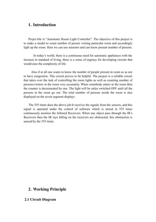
  • 1. 1. Introduction Projet title is “Automatic Room Light Controller”. The objective of this project is to make a model to count number of person visiting particular room and accordingly light up the room. Here we can use sensonrs and can know present number of persons. In today’s world, there is a continuous need for automatic appliances with the increase in standard of living, there is a sense of urgency for developing circuits that would ease the complexity of life. Also if at all one wants to know the number of people present in room so as not to have congestion. This circuit proves to be helpful. The project is a reliable circuit that takes over the task of controlling the room lights as well as counting number of persons/visitors in the room very accurately. When somebody enters in the room then the counter is decremented by one. The light will be onlye switched OFF until all the persons in the room go out. The total number of persons inside the room is also displayed on the seven segment displays. The 555 timer does the above job.It receives the signals from the sensors, and this signal is operated under the control of software which is stored in 555 timer continuously monitor the Infrared Receivers. When any object pass through the IR’s Receivers then the IR rays falling on the receivers are obstructed, this obstraction is sensed by the 555 timer. 2. Working Principle 2.1 Circuit Diagram
  • 2. There are two main part of the circuits. 1. Transmission Circuit(Infrared Led’s) 2. Receiver Circuit 1. Transmission Circuit This circuit diagram show how a 555 timer IC, configured to function as a basic astable multivibrator. The astable multivibrator generates a square wave, the period of which is determined by the circuit external to IC 555. The astable multivibrator does not require any external trigger to change the state of the output. Hence the name free running oscillator. The time during which the output is either high or low is
  • 3. determined by the two resistors and a capacitor which are externally connected to the 555 timer. IR Transmission circuit is used to generate the modulated 36 kHz IR signal. The IC555 in the transmitter side is to generate 36 kHz square wave. Adjust the preset in the transmitter to get a 38 kHz signal at the output. Then you point it over the sensors and its output will go low when it senses the IR signal of 38 kHz. 2. Receiver Circuit The IR transmitter will emit modulated 38 kHz IR signal and at the receiver we use TSPO1738(Infrared Sensor). The output goes high when there is an interruption and it return back to low after the time period determined by the capacitor and resistor in the circuit i.e. around 1 Second. CL100 is to trigger the IC555 which is configured as monostable multivibrator. Input is given to the port 1. Port 0 is user for the 7-Segment
  • 4. display purpose. Port 2 is used for the relay Turn on and Turn off purpose. LTS 542(Common Anode) is used for 7-Segment display and that time relay will get voltage and triggered, so light will get voltage and it will turn on and when counter will be 00 and at that time relay turned off. 2.2 PCB Layout 2.3 Components Lists 2.4 Working This system is designed by using two sets of IR transmitters and receivers. These IR sensors are placed in such a way that they detect a person entering and leaving the room to turn the home appliances. In this optimum energy management system, a microcontroller is the central processing unit of this project which is of 89S51
  • 5. controller from the 8051 family. This system facilitates a bidirectional visitor counter for displaying the number of persons inside the room. When a person enters into the room, an IR beam is obstructed between the IR transmitter and the receiver. This IR obstruction from the sensor-1 gives the corresponding signal to the microcontroller. The microcontroller in such a way that by the reception of the signal from the sensor-1 it turns on the fans and lights inside the room. Thus, the microcontroller gives command signals to a relay driver which turns the rellays such that all these appliances turn on. When the person leaves from this room, another set of IR sensors enable and give control signals to the microcontroller. Furthermore, similar to the above process, this system turns off the appliances like fans and lights. Apart from this, the system also takes account of the number of persons inside the room so that this control operation is varied depending on the persons’ availability in the room. For every person entering and leaving the room, the microcontroller reads the digital input from two receivers, and calculates the number of persons inside the room, and then displays it on the LCD. When the persons’ count is greater than one, the microcontroller turns on the room light and when the persons’ count is zero, it turns off all the lights and fans. 3. DESIGN PROCEDURE 3.1 Multivator A multivibrator circuit oscillates between a “HIGH” state and a “LOW” state producing a continuous output. Astable multivibrators generally have an even 50% duty cycle, that is that 50% of the cycle time the output is “HIGH” and the remaining 50% of the cycle time the output is “OFF”. In other words, the duty cycle for an astable timing pulse is 1:1. Sequential Logic Circuits that use the clock signal for synchronization are dependant upon the frequency and and clock pulse width to activate there switching action. Sequential circuits may also change their state on either the rising or falling edge, or both of the actual clock signal as we have seen previously with the basic flip-flop circuits. The following list are terms associated with a timing pulse or waveform. Active HIGH - if the state change occurs from a “LOW” to a “HIGH” at the clock’s pulse rising edge or during the clock width.
  • 6. Clock Signal Waveform Active LOW - if the state change occurs from a “HIGH” to a “LOW” at the clock’s pulses falling edge. Duty Cycle - this is the ratio of the clock width to the clock period. Clock Width - this is the time during which the value of the clock signal is equal to a logic “1”, or HIGH. Clock Period - this is the time between successive transitions in the same direction, ie, between two rising or two falling edges. Clock Frequency - the clock frequency is the reciprocal of the clock period, frequency = 1/clock period Clock pulse generation circuits can be a combination of analogue and digital circuits that produce a continuous series of pulses (these are called astable multivibrators) or a pulse of a specific duration (these are called monostable multivibrators). Combining two or more of multivibrators provides generation of a desired pattern of pulses (including pulse width, time between pulses and frequency of pulses). There are basically three types of clock pulse generation circuits: · Astable – A free-running multivibrator that has NO stable states but switches continuously between two states this action produces a train of square wave pulses at a fixed frequency. · Monostable – A one-shot multivibrator that has only ONE stable state and is triggered externally with it returning back to its first stable state. · Bistable – A flip-flop that has TWO stable states that produces a single pulse either positive or negative in value. One way of producing a very simple clock signal is by the interconnection of logic gates. As NANDgates contains amplification, they can also be used to provide a clock signal or timing pulse with the aid of a single Capacitor and a single Resistor to provide the feedback and timing function. These timing circuits are often used because of there simplicity and are also useful if a logic circuit is designed that has unused gates which can be utilised to create the monostable or astable oscillator. This simple type of RC Oscillator network is sometimes called a “Relaxation Oscillator”.
  • 7. 3.1 Operation: Figure 1: Basic BJT astable multivibrator The circuit has two astable (unstable) states that change alternatively with maximum transition rate because of the "accelerating" positive feedback. It is implemented by the coupling capacitors that instantly transfer voltage changes because the voltage across a capacitor cannot suddenly change. In each state, one transistor is switched on and the other is switched off. Accordingly, one fully charged capacitor discharges (reverse charges) slowly thus converting the time into an exponentially changing voltage. At the same time, the other empty capacitor quickly charges thus restoring its charge (the first capacitor acts as a time-setting capacitor and the second prepares to play this role in the next state). The circuit operation is based on the fact that the forward-biased base-emitter junction of the switched-on bipolar transistor can provide a path for the capacitor restoration. 3.2 State 1 (Q1 is switched on, Q2 is switched off): In the beginning, the capacitor C1 is fully charged (in the previous State 2) to the power supply voltage V with the polarity shown in Figure 1. Q1 is on and connects the left-hand positive plate of C1 to ground. As its right-hand negative plate is connected to Q2 base, a maximum negative voltage (-V) is applied to Q2 base that keeps Q2 firmly off. C1 begins discharging (reverse charging) via the high-value base resistor R2, so that the voltage of its right-hand plate (and at the base of Q2) is rising from below ground (-V) toward +V. As Q2 base-emitter junction is backward-biased, it does not conduct, so all the current from R2 goes into C1. Simultaneously, C2 that is fully discharged and even slightly charged to 0.6 V (in the previous State 2) quickly charges via the low-value collector resistor R4 and Q1 forward-biased base-emitter junction (because R4 is less than R2, C2 charges faster than C1). Thus C2 restores its charge and prepares for the next State C2 when it will act as a time-setting capacitor. Q1 is firmly saturated in the beginning by the "forcing" C2 charging current added to R3 current; in the end, only R3 provides the needed input base current. The resistance R3 is chosen small enough to keep Q1 (not deeply) saturated after C2 is fully charged.
  • 8. When the voltage of C1 right-hand plate (Q2 base voltage) becomes positive and reaches 0.6 V, Q2 base-emitter junction begins diverting a part of R2 charging current. Q2 begins conducting and this starts the avalanche-like positive feedback process as follows. Q2 collector voltage begins falling; this change transfers through the fully charged C2 to Q1 base and Q1 begins cutting off. Its collector voltage begins rising; this change transfers back through the almost empty C1 to Q2 base and makes Q2 conduct more thus sustaining the initial input impact on Q2 base. Thus the initial input change circulates along the feedback loop and grows in an avalanche-like manner until finally Q1 switches off and Q2 switches on. The forward-biased Q2 base-emitter junction fixes the voltage of C1 right-hand plate at 0.6 V and does not allow it to continue rising toward +V. 3.3 State 2 (Q1 is switched off, Q2 is switched on): Now, the capacitor C2 is fully charged (in the previous State 1) to the power supply voltage V with the polarity shown in Figure 1. Q2 is on and connects the right-hand positive plate of C2 to ground. As its left-hand negative plate is connected to Q1 base, a maximum negative voltage (-V) is applied to Q1 base that keeps Q1 firmly off. C2 begins discharging (reverse charging) via the high-value base resistor R3, so that the voltage of its left-hand plate (and at the base of Q1) is rising from below ground (-V) toward +V. Simultaneously, C1 that is fully discharged and even slightly charged to 0.6 V (in the previous State 1) quickly charges via the low-value collector resistor R1 and Q2 forward-biased base-emitter junction (because R1 is less than R3, C1 charges faster than C2). Thus C1 restores its charge and prepares for the next State 1 when it will act again as a time-setting capacitor...and so on... 3.4 Multivibrator frequency Derivation The duration of state 1 (low output) will be related to the time constant R2C1 as it depends on the charging of C1, and the duration of state 2 (high output) will be related to the time constant R3C2 as it depends on the charging of C2. Because they do not need to be the same, an asymmetric duty cycle is easily achieved. The voltage on a capacitor with non-zero initial charge is: Looking at C2, just before Q2 turns on, the left terminal of C2 is at the base-emitter voltage of Q1 (VBE_Q1) and the right terminal is at VCC ("VCC" is used here
  • 9. instead of "+V" to ease notation). The voltage across C2 is VCC minus VBE_Q1 . The moment after Q2 turns on, the right terminal of C2 is now at 0 V which drives the left terminal of C2 to 0 V minus (VCC - VBE_Q1) or VBE_Q1 - VCC. From this instant in time, the left terminal of C2 must be charged back up to VBE_Q1. How long this takes is half our multivibrator switching time (the other half comes from C1). In the charging capacitor equation above, substituting: VBE_Q1 for (VBE_Q1 - VCC) for VCC for results in: Solving for t results in: For this circuit to work, VCC>>VBE_Q1 (for example: VCC=5 V, VBE_Q1=0.6 V), therefore the equation can be simplified to: or or The period of each half of the multivibrator is therefore given by t = ln(2)RC. The total period of oscillation is given by: T = t1 + t2 = ln(2)R2 C1 + ln(2)R3 C2 where...
  • 10. · f is frequency in hertz. · R2 and R3 are resistor values in ohms. · C1 and C2 are capacitor values in farads. · T is the period (In this case, the sum of two period durations). For the special case where · t1 = t2 (50% duty cycle) · R2 = R3 · C1 = C2 3.5 Output pulse shape The output voltage has a shape that approximates a square waveform. It is considered below for the transistor Q1. During State 1, Q2 base-emitter junction is reverse-biased and the capacitor C1 is "unhooked" from ground. The output voltage of the switched-on transistor Q1 changes rapidly from high to low since this low-resistive output is loaded by a high impedance load (the series connected capacitor C1 and the high-resistive base resistor R2). During State 2, Q2 base-emitter junction is forward-biased and the capacitor C1 is "hooked" to ground. The output voltage of the switched-off transistor Q1 changes exponentially from low to high since this relatively high resistive output is loaded by a low impedance load (the capacitance C1). This is the output voltage of R1C1 integrating circuit. To approach the needed square waveform, the collector resistors have to be low resistance. The base resistors have to be low enough to make the transistors saturate in the end of the restoration (RB < β.RC). 3.6 Initial power-up: When the circuit is first powered up, neither transistor will be switched on. However, this means that at this stage they will both have high base voltages and therefore a tendency to switch on, and inevitable slight asymmetries will mean that one of the transistors is first to switch on. This will quickly put the circuit into one of the above states, and oscillation will ensue. In practice, oscillation always occurs for practical values of R and C.
  • 11. However, if the circuit is temporarily held with both bases high, for longer than it takes for both capacitors to charge fully, then the circuit will remain in this stable state, with both bases at 0.6 V, both collectors at 0 V, and both capacitors charged backwards to −0.6 V. This can occur at startup without external intervention, if R and C are both very small. 3.7 Frequency divider: An astable multivibrator can be synchronized to an external chain of pulses. A single pair of active devices can be used to divide a reference by a large ratio, however, the stability of the technique is poor owing to the variability of the power supply and the circuit elements; a division ratio of 10, for example, is easy to obtain but not dependable. Chains of bistable flip-flops provide more predictable division, at the cost of more active elements. 3.8 Protective components: While not fundamental to circuit operation, diodes connected in series with the base or emitter of the transistors are required to prevent the base-emitter junction being driven into reverse breakdown when the supply voltage is in excess of the Veb breakdown voltage, typically around 5-10 volts for general purpose silicon transistors. In the monostable configuration, only one of the transistors requires protection. 3.9 Astablemultivibrator: Astable Multivibrators are the most commonly used type of multivibrator circuit. An astable multivibrator is a free running oscillator that have no permanent “meta” or “steady” state but are continually changing there output from one state (LOW) to the other state (HIGH) and then back again. This continual switching action from “HIGH” to “LOW” and “LOW” to “HIGH” produces a continuous and stable square wave output that switches abruptly between the two logic levels making it ideal for timing and clock pulse applications. As with the previous monostable multivibrator circuit above, the timing cycle is determined by the RC time constant of the resistor-capacitor, RC Network. Then the output frequency can be varied by changing the value(s) of the resistors and capacitor in the circuit.
  • 12. NAND Gate Astable Multivibrator The astable multivibrator circuit uses two CMOS NOT gates such as the CD4069 or the 74HC04 hex inverter ICs, or as in our simple circuit below a pair of CMOS NAND such as the CD4011 or the 74LS132 and an RC timing network. The two NAND gates are connected as inverting NOT gates. Suppose that initially the output from the NAND gate U2 is HIGH at logic level “1”, then the input must therefore be LOW at logic level “0” (NAND gate principles) as will be the output from the first NAND gate U1. Capacitor, C is connected between the output of the second NAND gate U2 and its input via the timing resistor, R2. The capacitor now charges up at a rate determined by the time constant of R2 and C. As the capacitor, C charges up, the junction between the resistor R2 and the capacitor, C, which is also connected to the input of the NAND gate U1 via the stabilizing resistor, R2 decreases until the lower threshold value of U1 is reached at which point U1 changes state and the output of U1 now becomes HIGH. This causes NAND gate U2 to also change state as its input has now changed from logic “0” to logic “1” resulting in the output of NAND gate U2 becoming LOW, logic level “0”. Capacitor C is now reverse biased and discharges itself through the input of NAND gate U1. Capacitor, C charges up again in the opposite direction determined by the time constant of both R2and C as before until it reaches the upper threshold value of gate U1. This causes U1 to change state and the cycle repeats itself over again. Then, the time constant for a NAND gate Astable Multivibrator is given as T = 2.2RC in seconds with the output frequency given as f = 1/T. For example: if the resistor R2 = 10kΩ and the capacitor C = 45nF, the oscillation frequency of the circuit would be given as:
  • 13. Then the output frequency is calculated as being 1kHz, which equates to a time constant of 1mS so the output waveform would look like: 3.10 Monostablemultivibrator Circuit Monostable Multivibrators or “one-shot” pulse generators are generally used to convert short sharp pulses into wider ones for timing applications. Monostable multivibrators generate a single output pulse, either “HIGH” or “LOW”, when a suitable external trigger signal or pulse T is applied. This trigger pulse signal initiates a timing cycle which causes the output of the monostable to change state at the start of the timing cycle, ( t1 ) and remain in this second state until the end of the timing period, ( t2 ) which is determined by the time constant of the timing capacitor, CT and the resistor, RT. The monostable multivibrator now stays in this second timing state until the end of the RC time constant and automatically resets or returns itself back to its original (stable) state. Then, a monostable circuit has only one stable state. A more common name for this type of circuit is simply a “Flip-Flop” as it can be made from two cross-coupled NAND gates (or NOR gates) as we have seen previously. Consider the circuit below.
  • 14. Simple NAND Gate Monostable Circuit Suppose that initially the trigger input T is held HIGH at logic level “1” by the resistor R1 so that the output from the first NAND gate U1 is LOW at logic level “0”, (NAND gate principals). The timing resistor, RT is connected to a voltage level equal to logic level “0”, which will cause the capacitor, CT to be discharged. The output of U1 is LOW, timing capacitor CT is completely discharged therefore junction V1 is also equal to “0” resulting in the output from the second NAND gate U2, which is connected as an inverting NOT gate will therefore be HIGH. 3.11 Bistable Circuit: The Bistable Multivibrators circuit is basically a SR flip-flop that we look at in the previous tutorials with the addition of an inverter or NOT gate to provide the necessary switching function. As with flip-flops, both states of a bistable multivibrator are stable, and the circuit will remain in either state indefinitely. This type of multivibrator circuit passes from one state to the other “only” when a suitable external trigger pulse T is applied and to go through a full “SET-RESET” cycle twotriggering pulses are required. This type of circuit is also known as a “Bistable Latch“, “Toggle Latch” or simply “T-latch“. NAND Gate Bistable Multivibrator
  • 15. The simplest way to make a Bistable Latch is to connect together a pair of Schmitt NAND gates to form a SR latch as shown above. The two NAND gates, U2 and U3 form the bistable which is triggered by the input NAND gate, U1. This U1 NAND gate can be omitted and replaced by a single toggle switch to make a switch debounce circuit as seen previously in the SR Flip-flop tutorial. When the input pulse goes “LOW” the bistable latches into its “SET” state, with its output at logic level “1”, until the input goes “HIGH” causing the bistable to latch into its “RESET” state, with its output at logic level “0”. The output of a bistable multivibrator will stay in this “RESET” state until another input pulse is applied and the whole sequence will start again. Then a Bistable Latch or “Toggle Latch” is a two-state device in which both states either positive or negative, (logic “1” or logic “0”) are stable. Bistable Multivibrators have many applications such as frequency dividers, counters or as a storage device in computer memories but they are best used in circuits such as Latches and Counters. 4. 555 Timer 4.1 Introduction Simple Monostable or Astable multivibrators can now be easily made using standard commonly available waveform generator IC’s specially design to create timing and oscillator circuits. Relaxation oscillators can be constructed simply by connecting a few passive components to their input pins with the most commonly used waveform generator type IC being the classic 555 timer. The 555 Timer is a very versatile low cost timing IC that can produce a very accurate timing periods with good stability of around 1% and which has a variable timing period from between a few micro-seconds to many hours with the timing period being controlled by a single RC network connected to a single positive supply of between 4.5 and 16 volts. The NE555 timer and its successors, ICM7555, CMOS LM1455, DUAL NE556 etc, are covered in the555 Oscillator tutorial and other good electronics based websites, so are only included here for reference purposes as a clock pulse generator. The 555 connected as an Astable oscillator is given below.
  • 16. NE555 Astable Multivibrator. Here the 555 timer is connected as a basic Astable Multivibrator producing a continuous output waveform. Pins 2 and 6 are connected together so that it will re-trigger itself on each timing cycle, thereby functioning as an Astable oscillator. Capacitor, C1 charges up through resistor, R1 and resistor, R2 but discharges only through resistor, R2 as the other side of R2 is connected to the discharge terminal, pin 7. Then the timing period of t1 and t2 is given as: · t1 = 0.693 (R1 + R2) C1 · t2 = 0.693 (R2) C1 · T = t1 + t2 The voltage across the capacitor, C1 ranges from between 1/3 Vcc to approximately 2/3 Vcc depending upon the RC timing period. This type of circuit is very stable as it operates from a single supply rail resulting in an oscillation frequency which is independent of the supply voltage Vcc. In the next tutorial about Sequential Logic Circuits, we will look another type of clock controlled flop-flop called a Data Latch. Data latches are very useful sequential circuits which can be made from any standard gated SR flip-flop and used for frequency division to produce various ripple counters, frequency dividers and latches. 4.2 Inputs of 555/556: Trigger input: when < 1/3 Vs ('active low') this
  • 17. makes the output high (+Vs). It monitors the discharging of the timing capacitor in an astable circuit. It has a high input impedance > 2M . Threshold input: when > 2/3 Vs ('active high') this makes the output low (0V)*. It monitors the charging of the timing capacitor in astable and monostable circuits. It has a high input impedance > 10M . * providing the trigger input is > 1/3 Vs, otherwise the trigger input will override the threshold input and hold the output high (+Vs). Reset input: when less than about 0.7V ('active low') this makes the output low (0V), overriding other inputs. When not required it should be connected to +Vs. It has an input impedance of about 10k . Control input: this can be used to adjust the threshold voltage which is set internally to be 2/3 Vs. Usually this function is not required and the control input is connected to 0V with a 0.01μF capacitor to eliminate electrical noise. It can be left unconnected if noise is not a problem. The discharge pin is not an input, but it is listed here for convenience. It is connected to 0V when the timer output is low and is used to discharge the timing capacitor in astable and monostable circuits. 4.3 Output of 555/556: The output of a standard 555 or 556 can sink and source up to 200mA. This is more than most ICs and it is sufficient to supply many output transducers directly, including LEDs (with a resistor in series), low current lamps, piezo transducers, loudspeakers (with a capacitor in series), relay coils (with diode protection) and some motors (with diode protection). The output voltage does not quite reach 0V and +Vs, especially if a large current is flowing.
  • 18. To switch larger currents you can connect a transistor. The ability to both sink and source current means that two devices can be connected to the output so that one is on when the output is low and the other is on when the output is high. The top diagram shows two LEDs connected in this way. This arrangement is used in the Level Crossing project to make the red LEDs flash alternately. 4.4 Loudspeakers A loudspeaker (minimum resistance 64 ) may be connected to the output of a 555 or 556 astable circuit but a capacitor (about 100μF) must be connected in series. The output is equivalent to a steady DC of about ½Vs combined with a square wave AC (audio) signal. The capacitor blocks the DC, but allows the AC to pass as explained in capacitor coupling. Piezo transducers may be connected directly to the output and do not require a capacitor in series. 4.5 Duty Cycle of 555 Timer IC The duty cycle in a 555 integrated circuit (IC) is the percentage of time that the output is high for each cycle of the square wave. For example, if the total cycle time is 1 s and the output is high for the first 0.4 s of each cycle, the duty cycle is 40%. With an astable circuit, the duty cycle must always be greater than 50%. In other words, the duration for which the output is high must always be more than the duration during which the output is low.
  • 19. The explanation for this is pretty simple: For the duty cycle to be 50%, the capacitor would have to charge and discharge through the same resistance. The only way to accomplish that would be to omit R1 altogether, so that the capacitor charged and discharged through R2 only. But the problem with that is that you would end up connecting pin 7 directly to Vcc. With no resistance between pin 7 and the voltage source, the current flowing through pin 7 would exceed the maximum that can be handled by the circuitry inside the 555, and the chip would be damaged. There's a clever way around this limitation: Place a diode across R2. This diode bypasses R2 when the capacitor is charged. That way, the capacitor charges through R1 and discharges through R2. When a diode is used in this way, you have complete control over the duration of both the charge and discharge time. If R1 and R2 have the same value, the capacitor takes the same amount of time to charge as it does to discharge, so the duty cycle will be 50%. If R2 is smaller than R1, the duty cycle is less than 50% because the capacitor discharges faster than it charges. If you use this approach, you must adjust the formulas for calculating the time intervals as follows: T = 0.7 (R1 + R2) C1 Thigh = 0.7 R1 C1 Tlow = 0.7 R2 C1
  • 20. 4.6 Monostable: Schematic of a 555 in monostable mode
  • 21. The relationships of the trigger signal, the voltage on C and the pulse width in monostable mode In the monostable mode, the 555 timer acts as a "one-shot" pulse generator. The pulse begins when the 555 timer receives a signal at the trigger input that falls below a third of the voltage supply. The width of the output pulse is determined by the time constant of an RC network, which consists of a capacitor (C) and a resistor (R). The output pulse ends when the voltage on the capacitor equals 2/3 of the supply voltage. The output pulse width can be lengthened or shortened to the need of the specific application by adjusting the values of R and C.[5] The output pulse width of time t, which is the time it takes to charge C to 2/3 of the supply voltage, is given by where t is in seconds, R is in ohms (resistance) and C is in farads (capacitance). While using the timer IC in monostable mode, the main disadvantage is that the time span between any two triggering pulses must be greater than the RC time constant. 4.7 Bistable: Schematic of a 555 in bistable mode
  • 22. In bistable (also called Schmitt trigger) mode, the 555 timer acts as a basic flip-flop. The trigger and reset inputs (pins 2 and 4 respectively on a 555) are held high via pull-up resistors while the threshold input (pin 6) is simply floating. Thus configured, pulling the trigger momentarily to ground acts as a 'set' and transitions the output pin (pin 3) to Vcc (high state). Pulling the reset input to ground acts as a 'reset' and transitions the output pin to ground (low state). No timing capacitors are required in a bistable configuration. Pin 5 (control voltage) is connected to ground via a small-value capacitor (usually 0.01 to 0.1 uF); pin 7 (discharge) is left floating. 4.8 Astable: Standard 555 astable circuit In astable mode, the 555 timer puts out a continuous stream of rectangular pulses having a specified frequency. Resistor R1 is connected between VCC and the discharge pin (pin 7) and another resistor (R2) is connected between the discharge pin (pin 7), and the trigger (pin 2) and threshold (pin 6) pins that share a common node. Hence the capacitor is charged through R1 and R2, and discharged only through R2, since pin 7 has low impedance to ground during output low intervals of the cycle, therefore discharging the capacitor. In the astable mode, the frequency of the pulse stream depends on the values of R1, R2 and C: [8] The high time from each pulse is given by:
  • 23. and the low time from each pulse is given by: where R1 and R2 are the values of the resistors in ohms and C is the value of the capacitor in farads. The power capability of R1 must be greater than . Particularly with bipolar 555s, low values of must be avoided so that the output stays saturated near zero volts during discharge, as assumed by the above equation. Otherwise the output low time will be greater than calculated above. The first cycle will take appreciably longer than the calculated time, as the capacitor must charge from 0V to 2/3 of VCC from power-up, but only from 1/3 of VCC to 2/3 of VCC on subsequent cycles. To achieve a duty cycle of less than 50% a small diode (that is fast enough for the application) can be placed in parallel with R2, with the cathode on the capacitor side. This bypasses R2 during the high part of the cycle so that the high interval depends approximately only on R1 and C. The presence of the diode is a voltage drop that slows charging on the capacitor so that the high time is longer than the expected and often-cited ln(2)*R1C = 0.693 R1C. The low time will be the same as without the diode as shown above. With a diode, the high time is where Vdiode is when the diode has a current of 1/2 of Vcc/R1 which can be determined from its datasheet or by testing. As an extreme example, when Vcc= 5 and Vdiode= 0.7, high time = 1.00 R1C which is 45% longer than the "expected" 0.693 R1C. At the other extreme, when Vcc= 15 and Vdiode= 0.3, the high time = 0.725 R1C which is closer to the expected 0.693 R1C. The equation reduces to the expected 0.693 R1C if Vdiode= 0. The operation of RESET in this mode is not well defined, some manufacturers' parts will hold the output state to what it was when RESET is taken low, others will send the output either high or low. 4.9 Power on reset or Trigger:
  • 24. In VLSI devices, the power-on reset (PoR) is an electronic device incorporated into the integrated circuit that detects the power applied to the chip and generates a reset impulse that goes to the entire circuit placing it into a known state. A simple PoR uses the charging of a capacitor, in series with a resistor, to measure a time period during which the rest of the circuit is held in a reset state. A Schmitt trigger may be used to deassert the reset signal cleanly, once the rising voltage of the RC network passes the threshold voltage of the Schmitt trigger. The resistor and capacitor values should be determined so that the charging of the RC network takes long enough that the supply voltage will have stabilised by the time the threshold is reached. One of the issues with using RC network to generate PoR pulse is the sensitivity of the R and C values to the power-supply ramp characteristics. When the power supply ramp is rapid, the R and C values can be calculated so that the time to reach the switching threshold of the schmitt trigger is enough to apply a long enough reset pulse. When the power supply ramp itself is slow, the RC network tends to get charged up along with the power-supply ramp up. So when the input schmitt stage is all powered up and ready, the input voltage from the RC network would already have crossed the schmitt trigger point. This means that there might not be a reset pulse supplied to the core of the VLSI. 4.10 Edge-triggering: edge-triggering circuit If the trigger input is still less than 1/3 Vs at the end of the time period the output will remain high until the trigger is greater than 1/3 Vs. This situation can occur if the input signal is from an on-off switch or sensor. The monostable can be made edge triggered, responding only to changes of an input signal, by connecting the trigger signal through a capacitor to the trigger input. The capacitor passes sudden changes (AC) but blocks a constant (DC) signal. For further information please see the page on capacitance. The circuit is 'negative edge triggered' because it responds to a sudden fall in the input signal.
  • 25. The resistor between the trigger (555 pin 2) and +Vs ensures that the trigger is normally high (+Vs). 4.11 555/556 Inverting Buffer (Schmitt trigger) or NOT gate: 555 inverting buffer circuit (a NOT gate) NOT gate symbol The buffer circuit's input has a very high impedance (about 1M ) so it requires only a few μA, but the output can sink or source up to 200mA. This enables a high impedance signal source (such as an LDR) to switch a low impedance output transducer (such as a lamp). It is an inverting buffer or NOT gate because the output logic state (low/high) is the inverse of the input state: · Input low (< 1/3 Vs) makes output high, +Vs · Input high (> 2/3 Vs) makes output low, 0V When the input voltage is between 1/3 and 2/3 Vs the output remains in its present state. This intermediate input region is a deadspace where there is no response, a property called hysteresis, it is like backlash in a mechanical linkage. This type of circuit is called a Schmitt trigger. If high sensitivity is required the hysteresis is a problem, but in many circuits it is a helpful property. It gives the input a high immunity to noise because once the circuit output has switched high or low the input must change back by at least 1/3 Vs to make
  • 26. the output switch back. 4.12 Features · Direct replacement for SE555/NE555 · Timing from microseconds through hours · Operates in both astable and monostable modes · Adjustable duty cycle · Output can source or sink 200mA · Output and supply TTL compatible · Temperature and stability better than 0.005% · Normally on and off output 4.13 Applications · Precision timing · Pulse generation · Sequential timing · Time delay generation · Pulse width modulation · Linear ramp generator 5. Diodes: A diode is an electrical device allowing current to move through it in one direction with far greater ease than in the other. The most common kind of diode in modern circuit design is the semiconductor diode, although other diode technologies exist. Semiconductor diodes are symbolized in schematic diagrams such as Figure. The term “diode” is customarily reserved for small signal devices, I ≤ 1 A. The termrectifier is used for power devices, I > 1 A. Semiconductor diode schematic symbol: Arrows indicate the direction of electron current flow.
  • 27. When placed in a simple battery-lamp circuit, the diode will either allow or prevent current through the lamp, depending on the polarity of the applied voltage. Diode operation: (a) Current flow is permitted; the diode is forward biased. (b) Current flow is prohibited; the diode is reversed biased. When the polarity of the battery is such that electrons are allowed to flow through the diode, the diode is said to be forward-biased. Conversely, when the battery is “backward” and the diode blocks current, the diode is said to be reverse-biased. A diode may be thought of as like a switch: “closed” when forward-biased and “open” when reverse-biased. Oddly enough, the direction of the diode symbol's “arrowhead” points against the direction of electron flow. This is because the diode symbol was invented by engineers, who predominantly use conventional flow notation in their schematics, showing current as a flow of charge from the positive (+) side of the voltage source to the negative (-). This convention holds true for all semiconductor symbols possessing “arrowheads:” the arrow points in the permitted direction of conventional flow, and against the permitted direction of electron flow. Diode behavior is analogous to the behavior of a hydraulic device called a check valve. 5.1 Thermionic and gaseous state diodes: Thermionic diodes are thermionic-valve devices (also called as vacuum tubes, tubes, or valves), which are arrangements of electrodes surrounded by the vacuum within a glass envelope. Early examples were fairly alike in appearance to incandescent light bulbs. In the thermionic valve diodes, a current through heater filament indirectly heats cathode, another internal electrode treated with the mixture of barium and strontium oxides, which are the oxides of alkaline earth metals; these substances are taken because they have a small work function. (Some valves make use of direct heating, in which a tungsten filament acts as heater and cathode both.) The heat causes thermionic emission of the electrons into vacuum. In forward operation, a surrounding metal electrode known as anode is positively charged so that it
  • 28. electrostatically attracts emitted electrons. But the electrons are not easily released from unheated anode surface when the voltage polarity is reversed. Thus, any reverse flow is negligible. For much of 20th century, thermionic valve diodes were taken in use in analog signal applications, and as rectifiers in many power supplies. Nowadays, valve diodes are only used in niche applications like rectifiers in electric guitar and high-end audio amplifiers also a specialized high- voltage equipment. A thermionic diode is a thermionic-valve device (also known as a vacuum tube, tube, or valve), consisting of a sealed evacuated glass envelope containing two electrodes: a cathode heated by a filament, and a plate (anode). Early examples were fairly similar in appearance to incandescent light bulbs. In operation, a separate current through the filament (heater), a high resistance wire made of nichrome, heats the cathode red hot (800–1000 °C), causing it to release electrons into the vacuum, a process called thermionic emission. The cathode is coated with oxides of alkaline earth metals such as barium and strontium oxides, which have a low work function, to increase the number of electrons emitted. (Some valves use direct heating, in which a tungsten filament acts as both heater and cathode.) The alternating voltage to be rectified is applied between the cathode and the concentric plate electrode. When the plate has a positive voltage with respect to the cathode, itelectrostatically attracts the electrons from the cathode, so a current of electrons flows through the tube from cathode to plate. However when the polarity is reversed and the plate has a negative voltage, no current flows, because the cathode electrons are not attracted to it. The unheated plate does not emit any electrons itself. So electrons can only flow through the tube in one direction, from cathode to plate. In a mercury-arc valve, an arc forms between a refractory conductive anode and a pool of liquid mercury acting as cathode. Such units were made with ratings up to hundreds of kilowatts, and were important in the development of HVDC power transmission. Some types of smaller thermionic rectifiers sometimes had mercury vapor fill to reduce their forward voltage drop and to increase current rating over thermionic hard-vacuum devices. Throughout the vacuum tube era, valve diodes were used in analog signal applications and as rectifiers in DC power supplies in consumer electronics such as radios, televisions, and sound systems. They were replaced in power supplies beginning in the 1940s by selenium rectifiers and then by semiconductor diodes by the 1960s. Today they are still used in a few high power applications where their ability to withstand transients and their robustness gives them an advantage over semiconductor devices. The recent (2012) resurgence of interest among audiophiles and recording studios in old valve audio gear such as guitar amplifiers and home audio systems has provided a market for the legacy consumer diode valves.
  • 29. 5.2 I-V Characteristic Curves of Semiconductors: Semiconductor devices such as diodes, transistors and thyristors are all constructed using semiconductor PN junctions connected together and as such their I-V characteristics curves will reflect the operation of these PN junctions. Then these devices will have non-linear I-V characteristics, as opposed to resistors which have a linear relationship between the current and voltage. So for example, the primary function of a semiconductor diode is rectification of AC to DC. When a diode is forward biased (the higher potential is connected to its Anode), it will pass current. When the diode is reverse biased (the higher potential is connected to its Cathode), the current is blocked. Then a PN junction needs a bias voltage of a certain polarity and amplitude for current to flow. This bias voltage also controls the resistance of the junction and therefore the flow of current through it. Consider the diode circuit below. When the diode is forward biased, anode positive with respect to the cathode, a forward or positive current passes through the diode and operates in the top right quadrant of its I-V characteristics curves as shown. Starting at the zero intersection, the curve increases gradually into the forward quadrant but the forward current and voltage are extremely small. When the forward voltage exceeds the diodes P-N junctions internal barrier voltage, which for silicon is about 0.7 volts, avalanche occurs and the forward current increases rapidly for a very small increase in voltage producing a non-linear curve. The “knee” point on the forward curve.
  • 30. Fig Likewise, when the diode is reversed biased, cathode positive with respect to the anode, the diode blocks current except for an extremely small leakage current, and operates in the lower left quadrant of its I-V characteristic curves. The diode continues to block current flow through it until the reverse voltage across the diode becomes greater than its breakdown voltage point resulting in a sudden increase in reverse current producing a fairly straight line downward curve as the voltage losses control. This reverse breakdown voltage point is used to good effect with zener diodes. Then we can see that the I-V Characteristic Curves for a silicon diode are non-linear and very different to that of the previous resistors linear I-V curves as their electrical characteristics are different. Current-Voltage characteristics curves can be used to plot the operation of any electrical or electronic component from resistors, to amplifiers, to semiconductors and solar cells. The current-voltage characteristics of an electronic component tells us much about its operation and can be a very useful tool in determining the operating characteristics of a particular device or component by showing its possible combinations of current and voltage, and as a graphical aid can help visually understand better what is happening within a circuit. 6. Relay A relay is an electrically operated switch. Many relays use an electromagnet to mechanically operate a switch, but other operating principles are also used, such as solid-state relays. Relays are used where it is necessary to control a circuit by a low-power signal (with complete electrical isolation between control and controlled circuits), or where several circuits must be controlled by one signal. The first relays were used in long distance telegraph circuits as amplifiers: they repeated the signal coming in from one circuit and re-transmitted it on another circuit. Relays were used extensively in telephone exchanges and early computers to perform logical operations. A type of relay that can handle the high power required to directly control an electric motor or other loads is called a contactor. Solid-state relays control power circuits with no moving parts, instead using a semiconductor device to perform switching. Relays with calibrated operating characteristics and sometimes multiple operating coils are used to protect electrical circuits from overload or faults; in modern electric
  • 31. power systems these functions are performed by digital instruments still called "protective relays". Relay-lamp A simple electromagnetic relay consists of a coil of wire wrapped around a soft iron core, an iron yoke which provides a low reluctance path for magnetic flux, a movable iron armature, and one or more sets of contacts (there are two in the relay pictured). The armature is hinged to the yoke and mechanically linked to one or more sets of moving contacts. It is held in place by a spring so that when the relay is de-energized there is an air gap in the magnetic circuit. In this condition, one of the two sets of contacts in the relay pictured is closed, and the other set is open. Other relays may have more or fewer sets of contacts depending on their function. The relay in the picture also has a wire connecting the armature to the yoke. This ensures continuity of the circuit between the moving contacts on the armature, and the circuit track on the printed circuit board (PCB) via the yoke, which is soldered to the PCB. When an electric current is passed through the coil it generates a magnetic field that activates the armature, and the consequent movement of the movable contact(s) either makes or breaks (depending upon construction) a connection with a fixed contact. If
  • 32. the set of contacts was closed when the relay was de-energized, then the movement opens the contacts and breaks the connection, and vice versa if the contacts were open. When the current to the coil is switched off, the armature is returned by a force, approximately half as strong as the magnetic force, to its relaxed position. Usually this force is provided by a spring, but gravity is also used commonly in industrial motor starters. Most relays are manufactured to operate quickly. In a low-voltage application this reduces noise; in a high voltage or current application it reduces arcing. When the coil is energized with direct current, a diode is often placed across the coil to dissipate the energy from the collapsing magnetic field at deactivation, which would otherwise generate a voltage spike dangerous to semiconductor circuit components. Some automotive relays include a diode inside the relay case. Alternatively, a contact protection network consisting of a capacitor and resistor in series (snubber circuit) may absorb the surge. If the coil is designed to be energized with alternating current (AC), a small copper "shading ring" can be crimped to the end of the solenoid, creating a small out-of-phase current which increases the minimum pull on the armature during the AC cycle 6.1 Types Of Relays 1. Latching Relay Latching relays are also called impulse relays. They work in the bistable mode, and thus have two relaxing states. They are also called keep relays or stay relays because as soon as the current towards this relay is switched off, the relay continues the process that it was doing in the last state. This can be achieved only with a solenoid which is operating in a ratchet and cam mechanism. It can also be done by an over-centre spring mechanism or a permanent magnet mechanism in which, when the coil is kept in the relaxed point, the over-centre spring holds the armature and the contacts in the right spot. This can also be done with the help of a remanent core. In the ratchet and cam method, power consumption occurs only for a particular time. Hence it is more advantageous than the others. 2. Reed Relay These types of relays have been given more importance in the contacts. In order to protect them from atmospheric protection they are safely kept inside a vacuum or inert gas. Though these types of relays have a very low switching current and voltage ratings, they are famous for their switching speeds.
  • 33. 3. Polarized Relay This type of relay has been given more importance on its sensitivity. These relays have been used since the invention of telephones. They played very important roles in early telephone exchanges and also in detecting telegraphic distortion. The sensitivity of these relays are very easy to adjust as the armature of the relay is placed between the poles of a permanent magnet. 4. Buchholz Relay This relay is actually used as a safety device. They are used for knowing the amount of gas present in large oil-filled transformers. They are designed in such a way that they produce a warning if it senses either the slow production of gas or fast production of gas in the transformer oil. 5. Overload protection Relay As the name implies, these relays are used to prevent the electric motors from damage by over current and short circuits. For this the heating element is kept in series with the motor. Thus when over heat occurs the bi-metallic strip connected to the motor heats up and in turn releases a spring to operate the contacts of the relay. 6. Mercury Wetted Relay This relay is almost similar to the reed relay explained earlier. The only difference is that instead of inert gases, the contacts are wetted with mercury. This makes them more position sensitive and also expensive. They have to be vertically mounted for any operation. They have very low contact resistance and so can be used for timing applications. Due to these factors, this relay is not used frequently. 7. Machine Tool Relay This is one of the most famous industrial relay. They are mainly used for the controlling of all kinds of machines. They have a number of contacts with easily replaceable coils. This enabkes them to be easily converted from NO contact to NC contact. Many types of these relays can easily be setup in a control panel. Though they are very useful in industrial applications, the invention of PLC has made them farther away from industries. 8. Contacor Relay This is one of the most heavy load relay ever used. They are mainly used in switching electric motors. They have a wide range of current ratings from a few amps to hundreds. The contacts of these relays are usually made with alloys containing a small percentage of silver. This is done so as to avoid the hazardous effects of arcing. These type of relays are mainly categorized in the rough use areas. So, they produce loud noises while operated and hence cannot be used in places where noise is a problem.
  • 34. 9. Solid State relay SSR relays, as its name implies are designed with the help of solid state components. As they do not have any moving objects in their design they are known for their high reliability. 10. Solid State Contactor Relay These relays combine both the features of solid state relays and contactor relays. As a result they have a number of advantages. They have a very good heat sink and can be designed for the correct on-off cycles. They are mainly controlled with the help of PLC, micro-processors or microcontrollers. 7. Relay Applications In general, the point of a relay is to use a small amount of power in the electromagnet -- coming, say, from a small dashboard switch or a low-power electronic circuit -- to move an armature that is able to switch a much larger amount of power. For example, you might want the electromagnet to energize using 5 volts and 50 milliamps (250 milliwatts), while the armature can support 120V AC at 2 amps (240 watts). Relays are quite common in home appliances where there is an electronic control turning on something like a motor or a light. They are also common in cars, where the 12V supply voltage means that just about everything needs a large amount of current. In later model cars, manufacturers have started combining relay panels into the fuse box to make maintenance easier. For example, the six gray boxes in this photo of a Ford Windstar fuse box are all relays: In places where a large amount of power needs to be switched, relays are often cascaded. In this case, a small relay switches the power needed to drive a much larger relay, and that second relay switches the power to drive the load. Relays can also be used to implement Boolean logic. See How Boolean Logic Works for more information. Advantages The major advantage of a automatic light control system over stand-alone lighting controls or conventional manual switching is the ability to control individual lights or groups of lights from a single user interface device. This ability to control multiple light sources from a user device allows complex lighting scenes to be created. A room
  • 35. may have multiple scenes pre-set, each one created for different activities in the room. A major benefit of lighting control systems is reduced energy consumption. Longer lamp life is also gained when dimming and switching off lights when not in use. Wireless lighting control systems provide additional benefits including reduced installation costs and increased flexibility over where switches and sensors may be placed.