1. Sampling Theorem
1 Objective
This lab is designed to give you insight into the concepts of signal bandwidth and sampling theorem.
2 Pre-Lab
Before you go to the lab, read this handout entirely and study the circuit diagrams. When building your
circuits, be aware of the following guidelines:
• Build your circuits as neatly as possible.
• Label the inputs and outputs of each functional unit. This makes measurements and troubleshooting
much easier.
• Learn to think in the frequency domain. This is probably one of the first classes you have had in which
a large amount of the analysis is done in the frequency domain. Try to get a feel for the meaning of
the information on the TDS 7104 oscilloscope.
3 Procedure
3.1 Circuit Setup
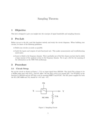
Set up the circuit as shown in Figure 1. X is an input signal from AFG310. The clock Clk is chosen to be
a 50 kHz pulse wave with 16 Vpp and 0 V offset. Set the duty cycle to be around 10%. Use PULS(E) as the
function in AFG310 and set the duty cycle by pressing SHIFT and FUNC. The DC power supplies for both
the ICs (MC14066 and 741) should be +8 V and −8 V.
Figure 1: Sampling Circuit
1
2. Figure 2: Low Pass Filter Circuit
3.2 Measurements
Use only TDS7104 oscilloscope to make both the time domain measurements and the frequency domain
measurements. Connect the output Y of the switch in Figure 1 to the input of the low pass filter circuit
shown in Figure 2. Measure and record the time waveforms and magnitude spectra at each of the following
points; have a 455 TA stamp these measurements,
1. X,
2. Y, and
3. Output of the Low Pass Filter.
Do this for the following Input Signals,
1. 1 kHz sine,
2. 40 kHz sine,
3. 1 kHz triangle, and
4. 40 kHz triangle.
4 Lab Deliverables (75 pts.)
Aliasing should be evident for 40 kHz signals in plots.
4 Time Plots (Sampling) Time domain plots of sampled 1 kHz and 40 kHz, sine and triangle input signals.
Each plot should have both input and sampled signal.
4 Spectrum Plots (Sampling) Magnitude spectrum plots of sampled 1 kHz and 40 kHz, sine and triangle
input signals.
4 Time Plots (Reconstruction) Time domain plots of sampled and reconstructed 1 kHz and 40 kHz, sine
and triangle input signals. Each plot should have input, sampled and reconstructed signal.
4 Spectrum Plots (Reconstruction) Magnitude spectrum plots of reconstructed 1 kHz and 40 kHz sine
and triangle input signals from sampled signals.
2
3. 5 Discussion Questions (25 pts.)
In the discussion section of your report, answer the following questions:
1. (5 pts.) How well could you recover the original input signals from the switch output? Was the
sampling frequency adequate for the input signals? Explain.
2. (5 pts.) Did you observe aliasing? Explain how you can identify whether a signal is being aliased.
3. (5 pts.) How did the cut-off frequency of the filter affect the output waveforms? Why did we use a low
pass filter for the signal reconstruction from samples? Explain.
4. (5 pts.) Explain how you will determine bandwidth of the input signals from the amplitude spectrum.
5. (5 pts.) Rank the four input signals in the order of increasing bandwidth. Explain your reasoning.
3