Bhubaneswar🌹Call Girls Bhubaneswar ❤Komal 9777949614 💟 Full Trusted CALL GIRL...
Internship PPT Template (1)_022402.ppt.x
1. A7441
–
Internship
-
I
VARDHAMAN COLLEGE OF ENGINEERING, HYDERABAD
Autonomous institute, affiliated to JNTUH
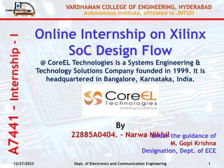
Online Internship on Xilinx
SoC Design Flow
@ CoreEL Technologies is a Systems Engineering &
Technology Solutions Company founded in 1999. It is
headquartered in Bangalore, Karnataka, India.
By
22885A0404. – Narwa Nikhil
Under the guidance of
M. Gopi Krishna
Designation, Dept. of ECE
12/27/2023 1
Dept. of Electronics and Communication Engineering
2. 12/27/2023 2
Dept. of Electronics and Communication Engineering
Certificate of Internship:
Xilinx SoC Design Flow
3. Xilinx SoC Design Flow
12/27/2023 3
Dept. of Electronics and Communication Engineering
Outline:
• Objectives (Crisp in 3-4 statements)
• History (Images)
• Introduction (Bullets with Images/Background knowledge)
• Architecture/Block Diagrams
• Methodology adapted in objectives achieved
• Skills (scientific and professional) learned during the internship
• Results/observations/work experiences
• Applications
• Conclusions
• References
4. 12/27/2023 4
Dept. of Electronics and Communication Engineering
Objectives:
Xilinx SoC Design Flow
• To master foundational
concepts of digital electronics,
combinational circuits and
sequential logic, VLSI design
flow.
• To gain expertise in Verilog
language constructs, data flow
and structural modeling, and
FPGA design using tools like
Vivado.
• To develop skills in functional
simulation techniques, FSM
design, and translating Verilog
code to FPGA bitstream for
practical deployment.
5. 12/27/2023 5
Dept. of Electronics and Communication Engineering
History:?
Xilinx SoC Design Flow
6. 12/27/2023 6
Dept. of Electronics and Communication Engineering
Introduction:
For example: Information collected from web, have to cite below mentioned
Source: VLSI Design - FPGA Technology (tutorialspoint.com)
Xilinx SoC Design Flow
During the course of my
internship, I explored the field of
digital electronics and design
methodologies. I gained
proficiency in combinational and
sequential logic circuits, refined
my abilities in Verilog HDL for
effective design and simulation,
and explored the intricacies of
FPGA design processes,
particularly with the Xilinx FPGA 7
families. Additionally, I gained
practical experience with the
Vivado Design Suite and gained
valuable insights into FPGA
implementation. This holistic
experience has deepened my
7. 12/27/2023 7
Dept. of Electronics and Communication Engineering
Architecture/Block Diagrams:
Xilinx SoC Design Flow
• CLB stands for Configurable
Logic Block in an FPGA.
• It's a fundamental unit that can be
tailored to perform specific logic
functions.
• CLBs offer flexibility, enabling
designers to customize logic as
per their application requirements.
• Wiring or pathways that allow for
connections between various
logic gates and storage elements
within the CLB.
8. 12/27/2023 8
Dept. of Electronics and Communication Engineering
Methodology adapted in objectives
achieved:
Xilinx SoC Design Flow
• Online Sessions &
Assignments:
Focus on digital basics, logic,
and VLSI flow.
Interactive slides, discussions,
real-world tasks.
• Verilog Deep Dive:
Explore constructs, data types,
and modelling.
Live coding with Vivado for
design and synthesis.
• Simulation & Design Flow:
Delve into FSM principles, FPGA
flows.
9. 12/27/2023 9
Dept. of Electronics and Communication Engineering
Skills (scientific and professional) learned
during the internship :
Xilinx SoC Design Flow
• Digital Design Expertise: Gain
foundational knowledge in digital
electronics and logic circuits.
• Verilog : Acquire skills in Verilog HDL for
both structural and behavioral modeling.
• Vivado design suite: Used for
designing, simulating, and synthesizing
FPGA-based digital systems.
• FPGA Application: Hands-on
experience with Xilinx FPGA 7 families
and Vivado for design and deployment.
10. 12/27/2023 10
Dept. of Electronics and Communication Engineering
Results/observations/work experiences:
Xilinx SoC Design Flow
11. 12/27/2023 11
Dept. of Electronics and Communication Engineering
Applications:
Xilinx SoC Design Flow
• Verilog is used for modeling and
simulating digital systems at
various levels of abstraction, from
gate-level to behavioral modeling,
• Verilog is extensively used for
designing ASIC’s for specific
applications such as in a consumer
electronics, automotive and
telecommunication.
• FPGA’s are used in test equipment
for generating signals, capturing
data, and performing real-time
analysis
• FPGA’s are integrated into
12. 12/27/2023 12
Dept. of Electronics and Communication Engineering
Conclusions:
Xilinx SoC Design Flow
This internship report delves into digital VLSI design,
encompassing Verilog HDL, FPGA design flow using Xilinx Vivado, and
the integration of Zynq SoC architecture. It highlights the synergy
between hardware and software through Xilinx Vitis, emphasizing
practical applications with Xilinx peripherals. The report underscores
the intersection of theoretical understanding and hands-on experience
in digital design, setting a foundation for future innovations in the field.
13. 12/27/2023 13
Dept. of Electronics and Communication Engineering
References:
[1] D. Pellerin, S. Thibault, Practical FPGA Programming in C (Prentice
Hall Professional Technical Reference, 2007)
[2] M. Boden, T. Fiebig, M. Reiband, and P. Reichel. 2008. GePaRD—A
high-level generation flow for partially reconfigurable designs. In
Proceedings of IEEE Computer Society Annual Symposium on VLSI
(ISVLSI).
[3] S. Brown, "FPGA architectural research: A survey", IEEE Des. Test.
Comput., vol. 13, no. 4, pp. 9-15, Winter 1996.
[4] S. Singh, "The Effect of Logic Block Architecture on FPGA
Performance", IEEE J. Solid-State Circuits, vol. 27, no. 3, pp. 281-287,
Mar. 1992.
Xilinx SoC Design Flow
14. 12/27/2023 14
Dept. of Electronics and Communication Engineering
Any
Questions/Discussion
s ???
Xilinx SoC Design Flow
15. 12/27/2023 15
Dept. of Electronics and Communication Engineering
Thank
You !!!
Xilinx SoC Design Flow