SlideShare a Scribd company logo
1 of 20
8086- Introduction
by vinod k dept of electronics
2
Intel 8086 Microprocessor
Key Features:
• Released by Intel in 1978
• Produced from 1978 to 1990s
• A 16-bit microprocessor chip.
• Max. CPU clock rate :
5 MHz to 10 MHz
• Package: 40 pin DIP
Fig1:Intel 8086 Microprocessor
3
8086 CPU Chip
Fig1: 8086 CPU Chip in DIP Package Fig2: CPU Chip
8086- Pin Diagram
Pin Details
AD0- AD15 : Bideirectional Address / Data Bus
A16- A19/ S3- S0 : Higher order address bus/ Segment identifier signals
Multiplex of Data and Address Lines
• Address lines A0-A7 and Data lines D0-D7 are
multiplexed in 8088. These lines are labelled as AD0-
AD7.
– By multiplexed we mean that the same pin carries
an address bit at one time and the data bit another
time.
Multiplex of Data and Address Lines
• Address lines A0-A15 and Data lines D0-D15 are multiplexed
in 8086. These lines are labeled as AD0-AD15.
GND
AD14
AD13
AD12
AD11
AD10
AD9
AD8
AD7
AD6
AD5
AD4
AD3
AD2
AD1
AD0
NMI
INTR
CLK
GND
VCC
AD15
A16/S3
A17/S4
A18/S5
A19/S6
HOLD
HLDA
ALE
READY
RESET
BHE/S7
MN/MX
RD
WR
M/IO
DT/R
DEN
INTA
TEST
1
2
3
4
5
6
7
8
9
10
11
12
13
14
15
16
17
18
19
20
31
30
29
28
27
26
25
24
23
22
21
40
39
38
37
36
35
34
33
32
8086
Minimum-mode and Maximum-mode
• 8088 and 8086 microprocessors can
be configured to work in either of the
two modes: the minimum mode and
the maximum mode
 Minimum mode:
 Pull MN/MX to logic 1
 Typically smaller systems and contains
a single microprocessor
 Cheaper since all control signals for
memory and I/O are generated by the
microprocessor.
 Maximum mode
 Pull MN/MX logic 0
 Larger systems with more than one
processor (designed to be used when a
coprocessor (8087) exists in the system)
GND
AD14
AD13
AD12
AD11
AD10
AD9
AD8
AD7
AD6
AD5
AD4
AD3
AD2
AD1
AD0
NMI
INTR
CLK
GND
VCC
AD15
A16/S3
A17/S4
A18/S5
A19/S6
HOLD
HLDA
ALE
READY
RESET
BHE/S7
MN/MX
RD
WR
M/IO
DT/R
DEN
INTA
TEST
1
2
3
4
5
6
7
8
9
10
11
12
13
14
15
16
17
18
19
20
31
30
29
28
27
26
25
24
23
22
21
40
39
38
37
36
35
34
33
32
8086
Lost Signals in
Max Mode
Minimum-mode and Maximum-mode
Signals
GND
AD14
AD13
AD12
AD11
AD10
AD9
AD8
AD7
AD6
AD5
AD4
AD3
AD2
AD1
AD0
NMI
INTR
CLK
GND
VCC
AD15
A16/S3
A17/S4
A18/S5
A19/S6
RQ/GT0
RQ/GT1
QS0
READY
RESET
BHE/S7
MN/MX
RD
LOCK
S2
S1
S0
QS1
TEST
1
2
3
4
5
6
7
8
9
10
11
12
13
14
15
16
17
18
19
20
31
30
29
28
27
26
25
24
23
22
21
40
39
38
37
36
35
34
33
32
8086
Max Mode
GND
AD14
AD13
AD12
AD11
AD10
AD9
AD8
AD7
AD6
AD5
AD4
AD3
AD2
AD1
AD0
NMI
INTR
CLK
GND
VCC
AD15
A16/S3
A17/S4
A18/S5
A19/S6
HOLD
HLDA
ALE
READY
RESET
BHE/S7
MN/MX
RD
WR
M/IO
DT/R
DEN
INTA
TEST
1
2
3
4
5
6
7
8
9
10
11
12
13
14
15
16
17
18
19
20
31
30
29
28
27
26
25
24
23
22
21
40
39
38
37
36
35
34
33
32
8086
Min Mode
Vcc GND
8086
CPU
F/C
AEN1
AEN2
Clock
generator
+5V
RES
Wait-State
Generator
CLK
READY
RESET
M/IO
INTA
RD
WR
PCLK
MN/MX +5V
STB
OE
8282
Latch
ALE
AD0-AD15
A16-A19
BHE BHE
D0 - D15
8286
DT/R
DEN
T
OE
16
A0 - A19
Address Bus
Control
Bus
8086 System Minimum mode
8086
CPU
Clock
generator
Wait-State
Generator
CLK
READY
RESET
MN/MX
AD0-AD15
A16-A19 BHE
STB
OE
8282
Latch
A0 - A19
Address Bus
+5V
RES
S0
S1
S2
CLK
S0
S1
S2
DATA
8286
Transceiver
T
OE
ALE
Gnd
DEN
DT/R
MRDC
MWTC
IORC
IOWC
AIOWC
AMWC
INTA
8288
Bus
Controller
8086 System Maximum Mode
Description of the Pins
GND
AD14
AD13
AD12
AD11
AD10
AD9
AD8
AD7
AD6
AD5
AD4
AD3
AD2
AD1
AD0
NMI
INTR
CLK
GND
VCC
AD15
A16/S3
A17/S4
A18/S5
A19/S6
RQ/GT0
RQ/GT1
QS0
READY
RESET
BHE/S7
MN/MX
RD
LOCK
S2
S1
S0
QS1
TEST
1
2
3
4
5
6
7
8
9
10
11
12
13
14
15
16
17
18
19
20
31
30
29
28
27
26
25
24
23
22
21
40
39
38
37
36
35
34
33
32
8086
Max Mode
GND
AD14
AD13
AD12
AD11
AD10
AD9
AD8
AD7
AD6
AD5
AD4
AD3
AD2
AD1
AD0
NMI
INTR
CLK
GND
VCC
AD15
A16/S3
A17/S4
A18/S5
A19/S6
HOLD
HLDA
ALE
READY
RESET
BHE/S7
MN/MX
RD
WR
M/IO
DT/R
DEN
INTA
TEST
1
2
3
4
5
6
7
8
9
10
11
12
13
14
15
16
17
18
19
20
31
30
29
28
27
26
25
24
23
22
21
40
39
38
37
36
35
34
33
32
8086
Min Mode
Vcc GND
CPU component Contents
Flags Cleared
Instruction Pointer 0000H
CS FFFFH
DS, SS and ES 0000H
Queue Empty
RESET Operation results
AD0 – AD15
Address
Data
AD0 - AD15: Address Data Bus
A17/S4 A16/S3 Function
0 0 Extra segment access
0 1 Stack segment access
1 0 Code segment access
1 1 Data segment access
A17/S4, A16/S3 Address/Status
A18/S5: The status of the
interrupt enable flag bit is updated
at the beginning of each cycle. The status of the flag
is indicated through this pin
A19/S6: When Low, it indicates that 8086 is in control
of the bus. During a "Hold acknowledge" clock
period, the 8086 tri-states the S6 pin and thus allows
another bus master to take control of the status bus.
A19/S6, A18/S5 Address/Status
S2 S1 S0 Characteristics
0 0 0
Interrupt
acknowledge
0 0 1 Read I/O port
0 1 0 Write I/O port
0 1 1 Halt
1 0 0 Code access
1 0 1 Read memory
1 1 0 Write memory
1 1 1 Passive State
S0, S1 and S2 Signals
QS1 QS1 Characteristics
0 0 No operation
0 1 First byte of opcode from queue
1 0 Empty the queue
1 1 Subsequent byte from queue
QS1 and QS2 Signals
IO/M DT/R SSO CHARACTERISTICS
0 0 0 Code Access
0 0 1 Read Memory
0 1 0 Write Memory
0 1 1 Passive
1 0 0 Interrupt Acknowledge
1 0 1 Read I/O port
1 1 0 Write I/O port
1 1 1 Halt
Read Write Control Signals
THANKS

More Related Content

What's hot

Pin digram of 8086
Pin digram of 8086Pin digram of 8086
Pin digram of 8086RJ
 
8086 pin details
8086 pin details8086 pin details
8086 pin detailsAJAL A J
 
American Fibertek MT0500A Data Sheet
American Fibertek MT0500A Data SheetAmerican Fibertek MT0500A Data Sheet
American Fibertek MT0500A Data SheetJMAC Supply
 
8086 in minimum mode
8086 in minimum mode8086 in minimum mode
8086 in minimum modeSridari Iyer
 
PIN Specification of 8086 Microprocessor
PIN Specification of 8086 MicroprocessorPIN Specification of 8086 Microprocessor
PIN Specification of 8086 MicroprocessorNikhil Kumar
 
Bus Structure, Memory and I/O Interfacing
Bus Structure, Memory and I/O InterfacingBus Structure, Memory and I/O Interfacing
Bus Structure, Memory and I/O InterfacingHetauda City College
 
TRAFFIC LIGHT CONTROL SYSTEM USING 8085 MICROPROCESSOR
TRAFFIC LIGHT CONTROL SYSTEM USING 8085 MICROPROCESSORTRAFFIC LIGHT CONTROL SYSTEM USING 8085 MICROPROCESSOR
TRAFFIC LIGHT CONTROL SYSTEM USING 8085 MICROPROCESSORSubash Sambath Kumar
 
I/o and memory interfacing
I/o and memory interfacingI/o and memory interfacing
I/o and memory interfacingRuchi Srivastava
 
8085 Interfacing with I/O Devices or Memory
8085 Interfacing with I/O Devices or Memory8085 Interfacing with I/O Devices or Memory
8085 Interfacing with I/O Devices or MemorySaumay Paul
 
Com 1288 Sf
Com 1288 SfCom 1288 Sf
Com 1288 Sfenenxx
 
Students corner131
Students corner131Students corner131
Students corner131Satti286
 
8279 in microprocessor
8279 in microprocessor8279 in microprocessor
8279 in microprocessorAisu
 
IM 42 XX Series - Intelligent Monitoring System - 4 to 20mA catalogue
IM 42 XX Series - Intelligent Monitoring System - 4 to 20mA catalogueIM 42 XX Series - Intelligent Monitoring System - 4 to 20mA catalogue
IM 42 XX Series - Intelligent Monitoring System - 4 to 20mA catalogueSuyash Lad
 

What's hot (19)

Pin digram of 8086
Pin digram of 8086Pin digram of 8086
Pin digram of 8086
 
8086 pin function
8086 pin function8086 pin function
8086 pin function
 
8086 pin details
8086 pin details8086 pin details
8086 pin details
 
American Fibertek MT0500A Data Sheet
American Fibertek MT0500A Data SheetAmerican Fibertek MT0500A Data Sheet
American Fibertek MT0500A Data Sheet
 
8086 microprocessor
8086 microprocessor8086 microprocessor
8086 microprocessor
 
8086 in minimum mode
8086 in minimum mode8086 in minimum mode
8086 in minimum mode
 
PIN Specification of 8086 Microprocessor
PIN Specification of 8086 MicroprocessorPIN Specification of 8086 Microprocessor
PIN Specification of 8086 Microprocessor
 
Bus Structure, Memory and I/O Interfacing
Bus Structure, Memory and I/O InterfacingBus Structure, Memory and I/O Interfacing
Bus Structure, Memory and I/O Interfacing
 
TRAFFIC LIGHT CONTROL SYSTEM USING 8085 MICROPROCESSOR
TRAFFIC LIGHT CONTROL SYSTEM USING 8085 MICROPROCESSORTRAFFIC LIGHT CONTROL SYSTEM USING 8085 MICROPROCESSOR
TRAFFIC LIGHT CONTROL SYSTEM USING 8085 MICROPROCESSOR
 
Chapter 5
Chapter 5Chapter 5
Chapter 5
 
I/o and memory interfacing
I/o and memory interfacingI/o and memory interfacing
I/o and memory interfacing
 
8085 Interfacing with I/O Devices or Memory
8085 Interfacing with I/O Devices or Memory8085 Interfacing with I/O Devices or Memory
8085 Interfacing with I/O Devices or Memory
 
Com 1288 Sf
Com 1288 SfCom 1288 Sf
Com 1288 Sf
 
Chapter5
Chapter5Chapter5
Chapter5
 
8086slide
8086slide8086slide
8086slide
 
Students corner131
Students corner131Students corner131
Students corner131
 
8279 in microprocessor
8279 in microprocessor8279 in microprocessor
8279 in microprocessor
 
Class5
Class5Class5
Class5
 
IM 42 XX Series - Intelligent Monitoring System - 4 to 20mA catalogue
IM 42 XX Series - Intelligent Monitoring System - 4 to 20mA catalogueIM 42 XX Series - Intelligent Monitoring System - 4 to 20mA catalogue
IM 42 XX Series - Intelligent Monitoring System - 4 to 20mA catalogue
 

Similar to Vino's 8086 introduction (20)

Microprocessors and Microcontrollers 8086 Pin Connections
Microprocessors and Microcontrollers 8086 Pin ConnectionsMicroprocessors and Microcontrollers 8086 Pin Connections
Microprocessors and Microcontrollers 8086 Pin Connections
 
2
22
2
 
microprocessor 8085
microprocessor 8085microprocessor 8085
microprocessor 8085
 
IO Interface (1).pptx
IO Interface (1).pptxIO Interface (1).pptx
IO Interface (1).pptx
 
Microprocessor
MicroprocessorMicroprocessor
Microprocessor
 
Badal sharma
Badal sharmaBadal sharma
Badal sharma
 
Chapter8-mikroprocessor
Chapter8-mikroprocessorChapter8-mikroprocessor
Chapter8-mikroprocessor
 
1st experiment ee 3214
1st experiment ee 32141st experiment ee 3214
1st experiment ee 3214
 
BUS DRIVER.pptx
BUS DRIVER.pptxBUS DRIVER.pptx
BUS DRIVER.pptx
 
8051 Presentation
8051 Presentation8051 Presentation
8051 Presentation
 
8255
82558255
8255
 
Advanced motion controls dzralte 012l080
Advanced motion controls dzralte 012l080Advanced motion controls dzralte 012l080
Advanced motion controls dzralte 012l080
 
Advanced motion controls dzralte 020l080
Advanced motion controls dzralte 020l080Advanced motion controls dzralte 020l080
Advanced motion controls dzralte 020l080
 
1346 A Single Chip Microcomputer
1346 A Single Chip Microcomputer1346 A Single Chip Microcomputer
1346 A Single Chip Microcomputer
 
2. 8085-Microprocessor.pptx
2. 8085-Microprocessor.pptx2. 8085-Microprocessor.pptx
2. 8085-Microprocessor.pptx
 
Microprocessor systems 8085(2)
Microprocessor systems 8085(2)Microprocessor systems 8085(2)
Microprocessor systems 8085(2)
 
Arc900 v1.1.8en
Arc900 v1.1.8enArc900 v1.1.8en
Arc900 v1.1.8en
 
Advanced motion controls dzcante 012l080
Advanced motion controls dzcante 012l080Advanced motion controls dzcante 012l080
Advanced motion controls dzcante 012l080
 
8155 GPPI
8155 GPPI8155 GPPI
8155 GPPI
 
Precision microcontrolleroverview
Precision microcontrolleroverviewPrecision microcontrolleroverview
Precision microcontrolleroverview
 

Recently uploaded

Beyond the EU: DORA and NIS 2 Directive's Global Impact
Beyond the EU: DORA and NIS 2 Directive's Global ImpactBeyond the EU: DORA and NIS 2 Directive's Global Impact
Beyond the EU: DORA and NIS 2 Directive's Global ImpactPECB
 
Russian Call Girls in Andheri Airport Mumbai WhatsApp 9167673311 💞 Full Nigh...
Russian Call Girls in Andheri Airport Mumbai WhatsApp  9167673311 💞 Full Nigh...Russian Call Girls in Andheri Airport Mumbai WhatsApp  9167673311 💞 Full Nigh...
Russian Call Girls in Andheri Airport Mumbai WhatsApp 9167673311 💞 Full Nigh...Pooja Nehwal
 
9548086042 for call girls in Indira Nagar with room service
9548086042  for call girls in Indira Nagar  with room service9548086042  for call girls in Indira Nagar  with room service
9548086042 for call girls in Indira Nagar with room servicediscovermytutordmt
 
social pharmacy d-pharm 1st year by Pragati K. Mahajan
social pharmacy d-pharm 1st year by Pragati K. Mahajansocial pharmacy d-pharm 1st year by Pragati K. Mahajan
social pharmacy d-pharm 1st year by Pragati K. Mahajanpragatimahajan3
 
Accessible design: Minimum effort, maximum impact
Accessible design: Minimum effort, maximum impactAccessible design: Minimum effort, maximum impact
Accessible design: Minimum effort, maximum impactdawncurless
 
Organic Name Reactions for the students and aspirants of Chemistry12th.pptx
Organic Name Reactions  for the students and aspirants of Chemistry12th.pptxOrganic Name Reactions  for the students and aspirants of Chemistry12th.pptx
Organic Name Reactions for the students and aspirants of Chemistry12th.pptxVS Mahajan Coaching Centre
 
1029 - Danh muc Sach Giao Khoa 10 . pdf
1029 -  Danh muc Sach Giao Khoa 10 . pdf1029 -  Danh muc Sach Giao Khoa 10 . pdf
1029 - Danh muc Sach Giao Khoa 10 . pdfQucHHunhnh
 
APM Welcome, APM North West Network Conference, Synergies Across Sectors
APM Welcome, APM North West Network Conference, Synergies Across SectorsAPM Welcome, APM North West Network Conference, Synergies Across Sectors
APM Welcome, APM North West Network Conference, Synergies Across SectorsAssociation for Project Management
 
microwave assisted reaction. General introduction
microwave assisted reaction. General introductionmicrowave assisted reaction. General introduction
microwave assisted reaction. General introductionMaksud Ahmed
 
SOCIAL AND HISTORICAL CONTEXT - LFTVD.pptx
SOCIAL AND HISTORICAL CONTEXT - LFTVD.pptxSOCIAL AND HISTORICAL CONTEXT - LFTVD.pptx
SOCIAL AND HISTORICAL CONTEXT - LFTVD.pptxiammrhaywood
 
Q4-W6-Restating Informational Text Grade 3
Q4-W6-Restating Informational Text Grade 3Q4-W6-Restating Informational Text Grade 3
Q4-W6-Restating Informational Text Grade 3JemimahLaneBuaron
 
1029-Danh muc Sach Giao Khoa khoi 6.pdf
1029-Danh muc Sach Giao Khoa khoi  6.pdf1029-Danh muc Sach Giao Khoa khoi  6.pdf
1029-Danh muc Sach Giao Khoa khoi 6.pdfQucHHunhnh
 
Mastering the Unannounced Regulatory Inspection
Mastering the Unannounced Regulatory InspectionMastering the Unannounced Regulatory Inspection
Mastering the Unannounced Regulatory InspectionSafetyChain Software
 
Interactive Powerpoint_How to Master effective communication
Interactive Powerpoint_How to Master effective communicationInteractive Powerpoint_How to Master effective communication
Interactive Powerpoint_How to Master effective communicationnomboosow
 
Separation of Lanthanides/ Lanthanides and Actinides
Separation of Lanthanides/ Lanthanides and ActinidesSeparation of Lanthanides/ Lanthanides and Actinides
Separation of Lanthanides/ Lanthanides and ActinidesFatimaKhan178732
 
BASLIQ CURRENT LOOKBOOK LOOKBOOK(1) (1).pdf
BASLIQ CURRENT LOOKBOOK  LOOKBOOK(1) (1).pdfBASLIQ CURRENT LOOKBOOK  LOOKBOOK(1) (1).pdf
BASLIQ CURRENT LOOKBOOK LOOKBOOK(1) (1).pdfSoniaTolstoy
 
Arihant handbook biology for class 11 .pdf
Arihant handbook biology for class 11 .pdfArihant handbook biology for class 11 .pdf
Arihant handbook biology for class 11 .pdfchloefrazer622
 

Recently uploaded (20)

Beyond the EU: DORA and NIS 2 Directive's Global Impact
Beyond the EU: DORA and NIS 2 Directive's Global ImpactBeyond the EU: DORA and NIS 2 Directive's Global Impact
Beyond the EU: DORA and NIS 2 Directive's Global Impact
 
Russian Call Girls in Andheri Airport Mumbai WhatsApp 9167673311 💞 Full Nigh...
Russian Call Girls in Andheri Airport Mumbai WhatsApp  9167673311 💞 Full Nigh...Russian Call Girls in Andheri Airport Mumbai WhatsApp  9167673311 💞 Full Nigh...
Russian Call Girls in Andheri Airport Mumbai WhatsApp 9167673311 💞 Full Nigh...
 
9548086042 for call girls in Indira Nagar with room service
9548086042  for call girls in Indira Nagar  with room service9548086042  for call girls in Indira Nagar  with room service
9548086042 for call girls in Indira Nagar with room service
 
social pharmacy d-pharm 1st year by Pragati K. Mahajan
social pharmacy d-pharm 1st year by Pragati K. Mahajansocial pharmacy d-pharm 1st year by Pragati K. Mahajan
social pharmacy d-pharm 1st year by Pragati K. Mahajan
 
Código Creativo y Arte de Software | Unidad 1
Código Creativo y Arte de Software | Unidad 1Código Creativo y Arte de Software | Unidad 1
Código Creativo y Arte de Software | Unidad 1
 
Accessible design: Minimum effort, maximum impact
Accessible design: Minimum effort, maximum impactAccessible design: Minimum effort, maximum impact
Accessible design: Minimum effort, maximum impact
 
Organic Name Reactions for the students and aspirants of Chemistry12th.pptx
Organic Name Reactions  for the students and aspirants of Chemistry12th.pptxOrganic Name Reactions  for the students and aspirants of Chemistry12th.pptx
Organic Name Reactions for the students and aspirants of Chemistry12th.pptx
 
1029 - Danh muc Sach Giao Khoa 10 . pdf
1029 -  Danh muc Sach Giao Khoa 10 . pdf1029 -  Danh muc Sach Giao Khoa 10 . pdf
1029 - Danh muc Sach Giao Khoa 10 . pdf
 
APM Welcome, APM North West Network Conference, Synergies Across Sectors
APM Welcome, APM North West Network Conference, Synergies Across SectorsAPM Welcome, APM North West Network Conference, Synergies Across Sectors
APM Welcome, APM North West Network Conference, Synergies Across Sectors
 
microwave assisted reaction. General introduction
microwave assisted reaction. General introductionmicrowave assisted reaction. General introduction
microwave assisted reaction. General introduction
 
SOCIAL AND HISTORICAL CONTEXT - LFTVD.pptx
SOCIAL AND HISTORICAL CONTEXT - LFTVD.pptxSOCIAL AND HISTORICAL CONTEXT - LFTVD.pptx
SOCIAL AND HISTORICAL CONTEXT - LFTVD.pptx
 
Q4-W6-Restating Informational Text Grade 3
Q4-W6-Restating Informational Text Grade 3Q4-W6-Restating Informational Text Grade 3
Q4-W6-Restating Informational Text Grade 3
 
1029-Danh muc Sach Giao Khoa khoi 6.pdf
1029-Danh muc Sach Giao Khoa khoi  6.pdf1029-Danh muc Sach Giao Khoa khoi  6.pdf
1029-Danh muc Sach Giao Khoa khoi 6.pdf
 
Mastering the Unannounced Regulatory Inspection
Mastering the Unannounced Regulatory InspectionMastering the Unannounced Regulatory Inspection
Mastering the Unannounced Regulatory Inspection
 
Interactive Powerpoint_How to Master effective communication
Interactive Powerpoint_How to Master effective communicationInteractive Powerpoint_How to Master effective communication
Interactive Powerpoint_How to Master effective communication
 
Mattingly "AI & Prompt Design: The Basics of Prompt Design"
Mattingly "AI & Prompt Design: The Basics of Prompt Design"Mattingly "AI & Prompt Design: The Basics of Prompt Design"
Mattingly "AI & Prompt Design: The Basics of Prompt Design"
 
Advance Mobile Application Development class 07
Advance Mobile Application Development class 07Advance Mobile Application Development class 07
Advance Mobile Application Development class 07
 
Separation of Lanthanides/ Lanthanides and Actinides
Separation of Lanthanides/ Lanthanides and ActinidesSeparation of Lanthanides/ Lanthanides and Actinides
Separation of Lanthanides/ Lanthanides and Actinides
 
BASLIQ CURRENT LOOKBOOK LOOKBOOK(1) (1).pdf
BASLIQ CURRENT LOOKBOOK  LOOKBOOK(1) (1).pdfBASLIQ CURRENT LOOKBOOK  LOOKBOOK(1) (1).pdf
BASLIQ CURRENT LOOKBOOK LOOKBOOK(1) (1).pdf
 
Arihant handbook biology for class 11 .pdf
Arihant handbook biology for class 11 .pdfArihant handbook biology for class 11 .pdf
Arihant handbook biology for class 11 .pdf
 

Vino's 8086 introduction

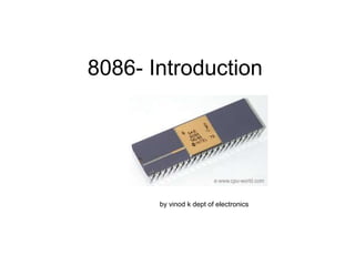
  • 1. 8086- Introduction by vinod k dept of electronics
  • 2. 2 Intel 8086 Microprocessor Key Features: • Released by Intel in 1978 • Produced from 1978 to 1990s • A 16-bit microprocessor chip. • Max. CPU clock rate : 5 MHz to 10 MHz • Package: 40 pin DIP Fig1:Intel 8086 Microprocessor
  • 3. 3 8086 CPU Chip Fig1: 8086 CPU Chip in DIP Package Fig2: CPU Chip
  • 5. Pin Details AD0- AD15 : Bideirectional Address / Data Bus A16- A19/ S3- S0 : Higher order address bus/ Segment identifier signals
  • 6. Multiplex of Data and Address Lines • Address lines A0-A7 and Data lines D0-D7 are multiplexed in 8088. These lines are labelled as AD0- AD7. – By multiplexed we mean that the same pin carries an address bit at one time and the data bit another time.
  • 7. Multiplex of Data and Address Lines • Address lines A0-A15 and Data lines D0-D15 are multiplexed in 8086. These lines are labeled as AD0-AD15. GND AD14 AD13 AD12 AD11 AD10 AD9 AD8 AD7 AD6 AD5 AD4 AD3 AD2 AD1 AD0 NMI INTR CLK GND VCC AD15 A16/S3 A17/S4 A18/S5 A19/S6 HOLD HLDA ALE READY RESET BHE/S7 MN/MX RD WR M/IO DT/R DEN INTA TEST 1 2 3 4 5 6 7 8 9 10 11 12 13 14 15 16 17 18 19 20 31 30 29 28 27 26 25 24 23 22 21 40 39 38 37 36 35 34 33 32 8086
  • 8. Minimum-mode and Maximum-mode • 8088 and 8086 microprocessors can be configured to work in either of the two modes: the minimum mode and the maximum mode  Minimum mode:  Pull MN/MX to logic 1  Typically smaller systems and contains a single microprocessor  Cheaper since all control signals for memory and I/O are generated by the microprocessor.  Maximum mode  Pull MN/MX logic 0  Larger systems with more than one processor (designed to be used when a coprocessor (8087) exists in the system) GND AD14 AD13 AD12 AD11 AD10 AD9 AD8 AD7 AD6 AD5 AD4 AD3 AD2 AD1 AD0 NMI INTR CLK GND VCC AD15 A16/S3 A17/S4 A18/S5 A19/S6 HOLD HLDA ALE READY RESET BHE/S7 MN/MX RD WR M/IO DT/R DEN INTA TEST 1 2 3 4 5 6 7 8 9 10 11 12 13 14 15 16 17 18 19 20 31 30 29 28 27 26 25 24 23 22 21 40 39 38 37 36 35 34 33 32 8086 Lost Signals in Max Mode
  • 9. Minimum-mode and Maximum-mode Signals GND AD14 AD13 AD12 AD11 AD10 AD9 AD8 AD7 AD6 AD5 AD4 AD3 AD2 AD1 AD0 NMI INTR CLK GND VCC AD15 A16/S3 A17/S4 A18/S5 A19/S6 RQ/GT0 RQ/GT1 QS0 READY RESET BHE/S7 MN/MX RD LOCK S2 S1 S0 QS1 TEST 1 2 3 4 5 6 7 8 9 10 11 12 13 14 15 16 17 18 19 20 31 30 29 28 27 26 25 24 23 22 21 40 39 38 37 36 35 34 33 32 8086 Max Mode GND AD14 AD13 AD12 AD11 AD10 AD9 AD8 AD7 AD6 AD5 AD4 AD3 AD2 AD1 AD0 NMI INTR CLK GND VCC AD15 A16/S3 A17/S4 A18/S5 A19/S6 HOLD HLDA ALE READY RESET BHE/S7 MN/MX RD WR M/IO DT/R DEN INTA TEST 1 2 3 4 5 6 7 8 9 10 11 12 13 14 15 16 17 18 19 20 31 30 29 28 27 26 25 24 23 22 21 40 39 38 37 36 35 34 33 32 8086 Min Mode Vcc GND
  • 11. 8086 CPU Clock generator Wait-State Generator CLK READY RESET MN/MX AD0-AD15 A16-A19 BHE STB OE 8282 Latch A0 - A19 Address Bus +5V RES S0 S1 S2 CLK S0 S1 S2 DATA 8286 Transceiver T OE ALE Gnd DEN DT/R MRDC MWTC IORC IOWC AIOWC AMWC INTA 8288 Bus Controller 8086 System Maximum Mode
  • 12. Description of the Pins GND AD14 AD13 AD12 AD11 AD10 AD9 AD8 AD7 AD6 AD5 AD4 AD3 AD2 AD1 AD0 NMI INTR CLK GND VCC AD15 A16/S3 A17/S4 A18/S5 A19/S6 RQ/GT0 RQ/GT1 QS0 READY RESET BHE/S7 MN/MX RD LOCK S2 S1 S0 QS1 TEST 1 2 3 4 5 6 7 8 9 10 11 12 13 14 15 16 17 18 19 20 31 30 29 28 27 26 25 24 23 22 21 40 39 38 37 36 35 34 33 32 8086 Max Mode GND AD14 AD13 AD12 AD11 AD10 AD9 AD8 AD7 AD6 AD5 AD4 AD3 AD2 AD1 AD0 NMI INTR CLK GND VCC AD15 A16/S3 A17/S4 A18/S5 A19/S6 HOLD HLDA ALE READY RESET BHE/S7 MN/MX RD WR M/IO DT/R DEN INTA TEST 1 2 3 4 5 6 7 8 9 10 11 12 13 14 15 16 17 18 19 20 31 30 29 28 27 26 25 24 23 22 21 40 39 38 37 36 35 34 33 32 8086 Min Mode Vcc GND
  • 13. CPU component Contents Flags Cleared Instruction Pointer 0000H CS FFFFH DS, SS and ES 0000H Queue Empty RESET Operation results
  • 14. AD0 – AD15 Address Data AD0 - AD15: Address Data Bus
  • 15. A17/S4 A16/S3 Function 0 0 Extra segment access 0 1 Stack segment access 1 0 Code segment access 1 1 Data segment access A17/S4, A16/S3 Address/Status
  • 16. A18/S5: The status of the interrupt enable flag bit is updated at the beginning of each cycle. The status of the flag is indicated through this pin A19/S6: When Low, it indicates that 8086 is in control of the bus. During a "Hold acknowledge" clock period, the 8086 tri-states the S6 pin and thus allows another bus master to take control of the status bus. A19/S6, A18/S5 Address/Status
  • 17. S2 S1 S0 Characteristics 0 0 0 Interrupt acknowledge 0 0 1 Read I/O port 0 1 0 Write I/O port 0 1 1 Halt 1 0 0 Code access 1 0 1 Read memory 1 1 0 Write memory 1 1 1 Passive State S0, S1 and S2 Signals
  • 18. QS1 QS1 Characteristics 0 0 No operation 0 1 First byte of opcode from queue 1 0 Empty the queue 1 1 Subsequent byte from queue QS1 and QS2 Signals
  • 19. IO/M DT/R SSO CHARACTERISTICS 0 0 0 Code Access 0 0 1 Read Memory 0 1 0 Write Memory 0 1 1 Passive 1 0 0 Interrupt Acknowledge 1 0 1 Read I/O port 1 1 0 Write I/O port 1 1 1 Halt Read Write Control Signals