SlideShare a Scribd company logo
1 of 25
Download to read offline
Linear Applicationssof
IC Op-Amps CHAPTER
3.1 INTRODUCTIOON
Integrated circuits (IC) are being used in a number ofelectronicapplications such as in the field of audio
and radio communication, medical electronics, instrumentation control ete. An important linear IC 1s
operational amplifier.
An operational amplifier (commonly referred to as op-amp) is a multi-terminal device whose
internal circuitry is quite complex. One of the reasons for the popularity of op-amps is its versatility
(used for ac as well as dc), in fact, the IC op-amp has characteristics that closely approach assumed
ideal op-amp.
3.2 CIRcUIT SYMBOY
The circuit symbol for the op-amp is a triangle as shown in Fig. 3.1.
+V
Positive Supply
Inverting
input
-o Output
Non-inverting o-
input
Negative Supply
V
Fig. 3.1 Circuit symbol of op-amp
An
op-amp has two inputs andoneoutput. The inputs are
markedwith minus (-) and plus (+) tospecify inverting and non-inverting inputs respectively. The two dc sources, named as +V and -V
are required for the biasing of op-amps, these two voltages are equal in magnitude with ôpposite
polarities.
n input applied at the non-inverting terminal will appear with same polarity at the output, while
an input applied to the inverting terminal will appear inverted (opposite) polarity at the output. )
33 EQUIVALENT CIRCUIT MODEL
ne equivalent circuit model ofan op-amp is shown in Fig. 3.b
Inverting
input U1
Ro
wUdR
Avd
Non-inverting
input
V2 -
Fig. 3.2 Equivalent circuit of op-amp
The output section consists of a voltage controlled source in series with the output resistance R,
It is evident from Fig. 3.2 that the input resistance R, is the Thevenin equivalent resistanceseen at
the input terminal. The differential input voltage v, is given by
...(3.1)
where v, = voltage between the inverting terminal and ground
V =voltage between the noninvertingterminal and ground
The op-amp senses the difference between the two inputs, multiplies it by the gain A, and causes
the resulting voltage to appear at the output. Thus, the output v, is given by
VAvd A(V2 V 3.2)
Where 4 is called the open-loop voltage gain (it 1S also represented as A) because it is the gainof the op-amp without any feedback from output to input.
/3.4 AN IDEAL OP-AMP
An ideal op-amp is an amplifier with infinite open-loop gain, infinite input resistance and zero outputanee An op-amp is ideal ifit has the rollowing characteristics. Also given in the table are
typical values of practical op-amps.
Characteristics Ideal op-amp
Practical op-ampP
Open loop gain (A)
104
Open loop bandwidth (BW)
=1MHz
Input impedance (Z
210 2Output impedance (Z,)
500 2
(Contd)
Linear pPp
Characteristics Ideal op-amp Practical op-amp
70 dB
Common Mode Rejection
Ratio (CMRR)
Input Offset voltage 0 < 10 mV
Input Offset current 0 <20nA
3.4.1 Important Characteristics of an ldeal Op-amp
For circuit analysis, an ideal op-amp is illustrated in Fig. 3.3.
i0 +
V2= 01
Fig. 3.3 ldeal op-amp model
The important characteristics of an ideal op-amp are
1. The current into both input terminals are zero
i0 and i,=0 ..(3.3)
This is due to infiniteinputresistance. An infinite rsistance between the input terminals implies
that an open circuit exists there and current cannot enter the op-amp
. The difference voltage across the input terminals is negligibly small
dV2V =0
Therefore, 1V2
...(3.4)
nus, an ideal op-amp has zero current into its two input terminals and negligibly small voltage
between two input terminals.
3.4.2 ldeal Voltage Transfer Curve
dge
A transfer curve may be defined as a curve which is drawn between input and output
ges.For op-amp the input voltage is v, and output is vo: A practical limitation of the op-amp 1s
magnitude of its output voltage cannot exceed | Vcc or |VIIn other words, theoupl
CS dependent and is limitedby the power supply voltage. Fig. 3.4 illustrates that the op-ampP
Operate inthree modes, depending on the differential input voltage Va
3.9 VOLTAGE TO CURRENT CONVERTER OR V-I cONVERTER
In a
voltage to current converter, the output load cuTent is proportional to the input voltage. Accordingto the connection of load there are twotypes of V to / converters:
Floating type and
Ground type.
In floating tvpe V to I converter R, 1s not connected to the ground whereas in grounded type. oneend of R, is connectedto the ground.
102
3.9.1 Voltage to Current Converter with Floating Load for ldeal Op-amn
accepts anVoltage to current converter (V-I converter) is also called a transconductance amplifier. It accserter in
input voltage v and produces an output current Fig. 5.15 shows a voltage to currentconvere
which load resistor R, is floating.
it is not connected
to physical ground
RL
RL w -
ww
-io
R
ww.
w
R - iVin
Voltage at these
terminal must be same
inirno current enter to
the op-amp
(b) Non-inverting configuration(a) Inverting configuration
Fig. 3.15 V-I converter for an ideal op-a
From Fig. 3.15(a) and (b)
As input current of op-amp is zero. The output current i, can be written as
Vin
i R ..(3.30
i,Vin ..(3.31
Thus the load current is always proportional to the input voltage and circuit works as voltage
current converter. The proportionality constant is generally 1/R,. Therefore, this circuit is also calle
transconductance amplifier. It is also called a voltage controlled current source (VCKS).
3.9.2 Voltage to Current Converter with Grounded Load for ldeal Op-amp
Figure 3.16 shows a voltage to current converter for ideal op-amp in which one end ofload resistor
IS grounded. It is also known as "Howland current converter from to name of its inventor.
The analysis of the circuit is accomplished by first determining the voltage v at the non-invertin
input terminal and then establishing the relationship between v, and the load current.
Apply KCL at node v, we get
i+iiL
in24 2 =
isR R
Linear
Applications of IC Op-Amps
inV 2v, = il
Yn+YiR
V
.(3.32)
2
R
R V1
w
ww-
Vo
R V2
www-
- i2R
RL V
Fig. 3.16 Voltage to current converter with grounded load
R
Rhe gain ofop-amp in non-inverting mode is given as A=1+ . for this circuit it is given as
follows
33)
A=1+
R
2
.(334)Hence output voltage can be written as
2
Substitute the equation (3.32) in equation (3.34)
R
-i, R
104
i R= Vn
(3.35)Vin
R
From the equation (3.35) we can say that the load current depends on the input voltage v and
resistor R.
An the current to voltage converter, the output voltage is proportional to the 1nput current. It accepts an
input current i, and produces an output voltage v,suchthatv =Ai, where A is the gain of the circuit.
Figure 3. 17 shows the current to voltage converter.
CURRENT TO VOoLTAGE cONVERTER OR -V CONVERTER
R
VoVa
O
Fig. 3.17 Current to voltage converter
The nodea is an virtual ground as node b is grounded.
.(3.36)
R R
..(3.37)V R
(3.38)o
The gain A is measured in ohms, it is more appropriate to denote gain by symbol R. Because of this.
I-V converters are also called ransresistance amplifiers.
This circuit is also referred as current controlled voltage source (CCVS). If the resistance in crcUl
is replaçed by the impedance, the cireuit is calicd transimpedance amplifier
GENERALIZED IMPEDANCE CONVERTER (GIC)
hpedance converters are active RC circuits designed to sinmulate frequency dependent elements suettas inductances for use in active filter synthesis. A simple general impedance converter (GlC) is show?in Fig. 3.18. It can be used not only to simulate inductances, but also to synthesize frequéney-dependentresistances.
ZZsZ Z
Fig. 3.18 Generalized impedance converter (GIC)
Find the equivalent impedance seen looking nto node A. We apply a test voltage as shown n
Fig. 3.19, we find the resulting current / and then Z -
VI.
Fach op-amp kecps (voltage at inverting and non-inverting terminal must be same), we
ha
labeled the voltages at the circuit nodes ofboth op-amps as By ohm's law we haNe
7
Summing currents at the node common to /, and,
a Circuits
106
V2
V
Z
V2V1
Z V
IIV
v
V1
Fig. 3.19 Finding equivalent impedance
Summing currents at the node common to Z and Z
V-V_ V-0
Z4 Z5
..(3.41)VV0- =o
ZsZ4
From equation (3.41)
V2
..(3.42)
Y r 2 + Z
From equation (3.39)
V- V=1Z
Substitute (V- V) in equation (3.40)
-IZ1 =0
Z3
.(3.43)
107Linear Applications of IC Op-Amps
Substituting V, from equation (3.42) in equation (3.43)
V(Z +Z4)_ IZ
Z325 Z Z
Z+Z-Z
Z,Zs
The impedance Z is defined as Z==44ils
...(3.44)
Z,Z4
Depending on the type of components we use for Z, through Z. We configure the circuit for various
impedance types.
3.11.1 Simulation of Inductars
Inthe generalized impedance converter, the Z, = Z, = Z, Zs = R and Z, is replaced by 1/sC as shown
in Fig. 3.20.
From Fig 3.20
Voltage at inverting and non-inverting terminal must be same, therefore, voltage at these terminal
represents V (see the analysis step 1, 2, 3 in Fig. 3.20).
Current entering into the op-amp is zero is identified in analysis steps 4, 5, 6 and 7 as shown in
Fig. 3.20.
Current through the capacitor is(as shown in analysis Step 8 of
Fig. 3.20)
Rs
Voltage at V, is analysed in step 9 of Fig. 3.20.
V2=V+
sC4 Rs
Current through the resistor R is 2 (see the analysis Step 10 of Fig. 3.20)
R3
V-V--
sC4 Rs=
R3 sR,RC4
108
Number with circle
represents analysis step.
A2
R3 1 / s C
V1 R2R www
V2 R11) 40
1
Rsv
A1
V1
Fig. 3.20 Inductance simulation circuit with analyzing steps
Current through resistor R, is same as the current passing through resistor R2.
In step 11, we determine the voltage V
V= V- R2
sRR,C4
.The current through R, is determined as follows (see the analysis step 12 as shown in Fig. 3
VRV-V +
sR,RC4 VRV-V=
R R sRR3RC4
From step 12, the total current entering into the circuit of Fig. 3.20.
VR ...3.4
sRR3R5CC4
The input impedance
=-sRRzR,C_ sL
R2
.(3.4
which is that of an inductance L given by
L RR,C
R2
.(3.4
ced
Note: We obtain the similar inductance function when the impedance Z,, Zz, Z,Z are
replaceby resistance and Z, =
1/sC, than the inductance becomes
L= RRsC
R
Linear Applications of lC Op-Amps
Filter is a frequency selective circuit that iscapable of passing signals with certain selected frequencies
while rejects signals of all other frequencies. This property ofa filter is called frequency selectivity.
Fig. 3.21 shows the classification of filters.
3.12 INTRODUCTION TO FILTERS
Filter
Digital filter Analog filter
Passive filterActive filter
Active RC filters Switched-capacitor filters.
Fig. 3.21 Classification of filters
Passive filters are constructed using inductors and capacitors, such filters work well at high frequencies.However, at low frequency the required inductors are large and physically bulky, and their characteristicsare quite non-ideal. Such inductors are impossible to fabricate in monolithic form and are
incompatiblewith modern techniques.
Active-RC filters employ op-amp with resistors and capacitors using discrete or hybrid thin-filmtechnology. Atthe present time, the most viable approach for real1zing full integrated monolithic filters isthe switched-capacitor technique.
dvantages of active filters over passive filter are
1. The maximum gain or the maximum value of the transfer function may be greater than unity.2. The loading effect is minimum, which means that the output response ofthe filter is independentof the load driven by the fitter.
3. Due to flexibility in gain and frequency adjustments, the active filters can be easily tuned.
3.12.1 Limitation of Active Filters. The finite bandwidth of the active devices place a limit on the highest frequency of operation..The important factor oftheactive filter is sensitivity. The active elements are much more sensitiveto the
temperature and the environmental changes than the passive elements. Hence due tochanges in the parameters due to the environmental changes, the active filter performance deviatesfrom its ideal response.
Active filter require dc power supply to operate it but the passive filter do not require the desupply.
OF SECOND ORDER FILTER3.15 GENERAL STRUCTURE
An improved transmission characteristics (frequency response) can be obtained by using a second
order active filter. A second order filter eonsists of two RC pairs and has a roll-off rate is
-40 dB/decade. A general second order filter (Sallen-key filter) is shown in Fig. 3.34.
R R
www- w
VA VB
Y YVi
A
1
Fig. 3.34 General structure of second order filter (Sallen-key model)
The op-amp is connected in non-inverting amplifier and hence
.(3.77)
-
A,VB
where A is the closed loop gain.
VB is the voltage at node B.
124
Apply KCL at node A is given
.3.
From equation(3.77), V andsubstitute v, in equation (3.78)
Ap
..(3
vY Y +
Y +
Ap
-v, Y
Apply KCL at node B is given
VAY2 gY +
Y)
AY2 (Y, +Y
Y2+Ya
A ( 3
Substituting equation (3.80) in equation (3.79) we get the voltage gain as
v,Y,= ( +Y2 +73)- Ap
-v,Y4, Y
( +YY +}, +¥)-Y¥2-4,Y,Y,|
Y(+2+%)+Y,(+Y2 +Y)-Y2Y -4,Y,Y
Ap2
+Yh +YY3 +Y4(K +Y2+Ys)-Y^Y'2 -ApY^Y|Vo ApY2
YY +Y(Y% +Y2 +Y)+ Y,Y(1- 4,)
.(3.81)T .
Yy+ Ya(} + Y2 + Y) + Y2¥3(1 -4,)
3.15.1 Second Order Low Pass Filte
Using Sallen-key model a second order low pass filter can be formed, if we set equal value of R and C
for simplicity. Fig. 3.35 shows the second order low pass filter.
Ri Ri
ww www-
R1 R2 OVo
ww ww
C CL
Fig. 3.35 Second order low pass fiter
From Fig. 3.35. Let we consider
Y h=sC; and Y, =sC2
R R
Substitute above values in equation (3.81)
Ap R R
T(s)
+sC R R2 0-44)R R
Integr
126
Ap
(RR+R2+sRR2C + sRC(1 4,)
RR21+sRRC2
Ap
14sC, (R + R,)+s2R,R,CC2+sR{C1 4p
A,/R,R,CC2
s(RC2 + R,C2 +RCi(1-4,)
RRCC2
1T(s) =
RRCC2
Note: For simplicity we consider R, =
R, =
R and C, =
C, =
C the two equation (3.83)
Ap
1+sC(2R)+s*R-C?+sRC(1=A,)
Ts)=
ApT 2R?c2+sRC(3-A,)+1
From equation (3.84) we conclude that
) For low frequencyf= 0 (s =
0)
T(0)=Ap
(i) For high frequency f= (s =
oo
T(oo)= 0
it shows that the frequency response is look like LPF.
3.15.4HigherOrderButterworthFilters
FilterswhichuseButterworthpolynomialsarecalledButterworthfiltersalsocalledasmaximallyfls
filters.IfB(s)isaButterworthpolynomialwhosemagnitudeisgivenby
2n
B(0)=1+.3.98)
whereocoverfrequency
n=orderofthefilter
Table3.2givestheButterworthpolynomialsB.(s)upto6thorderwiththehelpoftheirpolynononecandesignafilterofdesiredorder.
nials
Table3.2Batterworthpolynomials
Factorsofpolynomials
s+1
2s+1.414s+1
(s+1)(+s+1)
(s2+0.765s+1)(s2+1.848s+1)
(s+1)(s+0.618s+1)(s+1.618s+1)
(s+0.518s+1)(s+1.414s+1)(s+1.932s+1)
5
6
A band-pass filter passes all those frequencies lying with in a band between a lower-cut-off frequency
(S) and a higher cut-off frequency (p) and rejects or attenuate all other frequencies outside this
specified band. A generalized band pass response is shown in Fig. 3.41.
36 BAND PASS FILTERS
Gain
Ap
0.707 Ap
f(Hz)
fo f
Fig. 3.41 Frequency response of band pass filter
The difference betweenfy andff (>S) is the bandwidth of a band pass filter. As we know, the
quality factor of any filter is measure of selectivity of that filter means the higher the value of . The
band pass filter can be classified based on Q.
1. Narrow band pass filter (> 10)
2. Wide band pass filter (10)
The quality factor of a band pass filter is the ratio of centre frequency () to the bandwidth (BW)
Jo= -
BW 4i u
o ...(3.104)
where bandwidth BW=Iu-J The centre frequency
fo- NSHfL .(3.105)
The quality factor (O) can also be expressed in terms of damping coefficient of a filter
Ste
.(3.106)
3.16.1 Structure ofBand pass Filter
A band pass filter can be formed by cascading high pass and low pass filter as shown in Fig. 3.42. Th
cut-off frequency or corner frequency of high pass filter (/) must be higher than corner frequenc)
f) of low pass filter.
High pass
filter (f)
Low paSS
filter (fH) VoutVi
High-pass Low pass
sectionsection
Fig. 3.42 Structure of band pass filter
3.17 BAND STOP FILTER
Band stop filter or band elimination filters stops the frequencies in the stop band and pass all other
frequencies outside the stop-band
Types of Band stop filter
1. Wide band stop filter (< 10)
2. Narrow band stop filter (Q> 10) or notch filter
The O ofthe narrow band stop filter is high and they are known as the notch filter. Due to large value
of O, the bandwidth of band stop filter is smaller than that of the wide band stop filter
3.17.1 Wide Band-Stop Filter
Figure 3.47 shows the block diagram of wide band-stop filter and it consist of a low pass filter, a high
pass filter and summing amplifier.
In order to practically obtain the frequency of a wide band stop filter, we have to adjust the cut-off
irequencyf, of high pass filter is higher than the cut-off frequencyf 0f low pass filter.
..(3.128)For band stop filter
wide band stop
filter response
L
Highpass
filter
H fL
Summing
amplifier
Vo
Vin
fHfLLowpass
filter
Fig. 3.47 Block diagram of wide band-stop filter
Fig. 3.48 shows the wide band-stop filter using three op-amp
RF
High pass
filterR1
R4R2
ww
www
Summing
amplifier
C
R R3
o Vout
RR
2 RoM
C A2
Low pass
filterw
R'F
R1
Fig. 3.48 Wide band-stop filter
The combined frequency response ofis shown in Fig. 3.49. Another important constraint is that the
passband of the lowpass and high pass filters should be identical. The centre frequency is given by
...(3.129)
Gain
Pass band Stop band Pass band
f cut-offfrequency of HPF
G fH Cut-offfrequency of LPF
0.707 G
Frequency
response of LPF
fH fo L
Frequency response
of HPF
Fig. 3.49 Frequency response of wide band-stop filter
3.19 ALL PASS FILTR But
The filters which are discussedlused to adjust the magnitude ofthe transfer functionof thecircul
nis also alters the phase angle characteristics of the circuit. It is many times required to cOnuo
phase response of the filter.
The filter which is used to control the phase response by adding a phase shift between input and
Output signals is called as all pass filter. Its gain is one for all thefrequencies.
Thus, as the name suggests, it passes all the frequencies of the input Signal. It does not procduoe
attenuation but provide the required phase shift for the different frequencies ofthe input signal. Fio 3
shows the simple first order all pass filter.
ice:any
signal.Fig.3.
158
R= R1
R B
o Vo
V O A
ww-
R
Fig. 3.52 All pass filter
Analysis of the Circuit
Let us use the superposition principle to obtain the expression for the output voltage v,. Fig. 3.53(a) and
(6) shows the circuit with consideration ofone input connected to input and other input is made ground.
Assume input to the non-inverting terminal zero as shown in Fig. 3.53(a). The circuit acts as an
invertingamplifier
R RR
wwR R1
O Vo2
R
VAViO ww
ViO- ww
Vo
1/sC
(a)
(b)
Fig.3.53
R -VË
R
Vol
Vol-V when R-R ...(3.132)

More Related Content

What's hot (20)

Rectifier
RectifierRectifier
Rectifier
 
Power amplifier
Power amplifierPower amplifier
Power amplifier
 
Feedback amplifiers
Feedback  amplifiersFeedback  amplifiers
Feedback amplifiers
 
Amplifier (Transformer Coupled)
Amplifier (Transformer Coupled)Amplifier (Transformer Coupled)
Amplifier (Transformer Coupled)
 
14699775563. feedback amplifiers
14699775563. feedback amplifiers14699775563. feedback amplifiers
14699775563. feedback amplifiers
 
Differential amplifier
Differential amplifierDifferential amplifier
Differential amplifier
 
Pll ppt
Pll pptPll ppt
Pll ppt
 
Transmission lines
Transmission linesTransmission lines
Transmission lines
 
Ssb generation method
Ssb generation methodSsb generation method
Ssb generation method
 
Operational Amplifier Part 1
Operational Amplifier Part 1Operational Amplifier Part 1
Operational Amplifier Part 1
 
Transistor configurations
Transistor configurationsTransistor configurations
Transistor configurations
 
Active and passive
Active and passiveActive and passive
Active and passive
 
Inductors
InductorsInductors
Inductors
 
EC6202 ELECTRONIC DEVICES AND CIRCUITS NOTES
EC6202 ELECTRONIC DEVICES AND CIRCUITS NOTESEC6202 ELECTRONIC DEVICES AND CIRCUITS NOTES
EC6202 ELECTRONIC DEVICES AND CIRCUITS NOTES
 
DAC-digital to analog converter
DAC-digital to analog converterDAC-digital to analog converter
DAC-digital to analog converter
 
Basics of amplifier
Basics of amplifierBasics of amplifier
Basics of amplifier
 
Cro cathode ray oscilloscope working and applications
Cro cathode ray oscilloscope working and applicationsCro cathode ray oscilloscope working and applications
Cro cathode ray oscilloscope working and applications
 
Transistor basics
Transistor   basicsTransistor   basics
Transistor basics
 
Final
FinalFinal
Final
 
Op amp comparator
Op amp comparatorOp amp comparator
Op amp comparator
 

Similar to Integrated circuit unit 2 notes

Electronic circuit design lab manual
Electronic circuit design lab manualElectronic circuit design lab manual
Electronic circuit design lab manualawais ahmad
 
OPERATIONAL AMPLIFIERS
OPERATIONAL AMPLIFIERSOPERATIONAL AMPLIFIERS
OPERATIONAL AMPLIFIERSTamilarasan N
 
Chapter 7: Operational Amplifier (Op-Amp)
Chapter 7: Operational Amplifier (Op-Amp)Chapter 7: Operational Amplifier (Op-Amp)
Chapter 7: Operational Amplifier (Op-Amp)JeremyLauKarHei
 
Bipolar junction transistor characterstics biassing and amplification, lab 9
Bipolar junction transistor characterstics biassing and amplification, lab 9Bipolar junction transistor characterstics biassing and amplification, lab 9
Bipolar junction transistor characterstics biassing and amplification, lab 9kehali Haileselassie
 
Analog IC Application
Analog IC ApplicationAnalog IC Application
Analog IC ApplicationTamilarasan N
 
Unit-I Characteristics of opamp
Unit-I Characteristics of opampUnit-I Characteristics of opamp
Unit-I Characteristics of opampDr.Raja R
 
Power amplifiers analog electronics.pptx
Power amplifiers analog electronics.pptxPower amplifiers analog electronics.pptx
Power amplifiers analog electronics.pptxPrateek718260
 
Circuit theory 1 finals
Circuit theory 1 finalsCircuit theory 1 finals
Circuit theory 1 finalsjerbor
 
Circuit theory 1 finals
Circuit theory 1 finalsCircuit theory 1 finals
Circuit theory 1 finalsjerbor
 
Impulse test for power transformers
Impulse test for power transformersImpulse test for power transformers
Impulse test for power transformersjibinjoy1988
 
L08 power amplifier (class a)
L08 power amplifier (class a)L08 power amplifier (class a)
L08 power amplifier (class a)Sarah Krystelle
 
Short notes on digital electronics for specialist officer it exam by das sir,...
Short notes on digital electronics for specialist officer it exam by das sir,...Short notes on digital electronics for specialist officer it exam by das sir,...
Short notes on digital electronics for specialist officer it exam by das sir,...Tamal Kumar Das
 

Similar to Integrated circuit unit 2 notes (20)

Op-amp.pptx
Op-amp.pptxOp-amp.pptx
Op-amp.pptx
 
Electronic circuit design lab manual
Electronic circuit design lab manualElectronic circuit design lab manual
Electronic circuit design lab manual
 
OPERATIONAL AMPLIFIERS
OPERATIONAL AMPLIFIERSOPERATIONAL AMPLIFIERS
OPERATIONAL AMPLIFIERS
 
Chapter 7: Operational Amplifier (Op-Amp)
Chapter 7: Operational Amplifier (Op-Amp)Chapter 7: Operational Amplifier (Op-Amp)
Chapter 7: Operational Amplifier (Op-Amp)
 
Op amp
Op ampOp amp
Op amp
 
Bipolar junction transistor characterstics biassing and amplification, lab 9
Bipolar junction transistor characterstics biassing and amplification, lab 9Bipolar junction transistor characterstics biassing and amplification, lab 9
Bipolar junction transistor characterstics biassing and amplification, lab 9
 
Bipolar junction transistor characterstics biassing and amplification, lab 9
Bipolar junction transistor characterstics biassing and amplification, lab 9Bipolar junction transistor characterstics biassing and amplification, lab 9
Bipolar junction transistor characterstics biassing and amplification, lab 9
 
Lesson4
Lesson4Lesson4
Lesson4
 
Peakdetector
PeakdetectorPeakdetector
Peakdetector
 
Analog IC Application
Analog IC ApplicationAnalog IC Application
Analog IC Application
 
Unit-I Characteristics of opamp
Unit-I Characteristics of opampUnit-I Characteristics of opamp
Unit-I Characteristics of opamp
 
UNIT-3 OPAMP.pptx
UNIT-3 OPAMP.pptxUNIT-3 OPAMP.pptx
UNIT-3 OPAMP.pptx
 
OP-AMP.pptx
OP-AMP.pptxOP-AMP.pptx
OP-AMP.pptx
 
Power amplifiers analog electronics.pptx
Power amplifiers analog electronics.pptxPower amplifiers analog electronics.pptx
Power amplifiers analog electronics.pptx
 
Circuit theory 1 finals
Circuit theory 1 finalsCircuit theory 1 finals
Circuit theory 1 finals
 
Circuit theory 1 finals
Circuit theory 1 finalsCircuit theory 1 finals
Circuit theory 1 finals
 
Impulse test for power transformers
Impulse test for power transformersImpulse test for power transformers
Impulse test for power transformers
 
L08 power amplifier (class a)
L08 power amplifier (class a)L08 power amplifier (class a)
L08 power amplifier (class a)
 
Short notes on digital electronics for specialist officer it exam by das sir,...
Short notes on digital electronics for specialist officer it exam by das sir,...Short notes on digital electronics for specialist officer it exam by das sir,...
Short notes on digital electronics for specialist officer it exam by das sir,...
 
EE101 Lab4 Guillemaud
EE101 Lab4 GuillemaudEE101 Lab4 Guillemaud
EE101 Lab4 Guillemaud
 

Recently uploaded

Past, Present and Future of Generative AI
Past, Present and Future of Generative AIPast, Present and Future of Generative AI
Past, Present and Future of Generative AIabhishek36461
 
Call Girls Delhi {Jodhpur} 9711199012 high profile service
Call Girls Delhi {Jodhpur} 9711199012 high profile serviceCall Girls Delhi {Jodhpur} 9711199012 high profile service
Call Girls Delhi {Jodhpur} 9711199012 high profile servicerehmti665
 
VIP Call Girls Service Hitech City Hyderabad Call +91-8250192130
VIP Call Girls Service Hitech City Hyderabad Call +91-8250192130VIP Call Girls Service Hitech City Hyderabad Call +91-8250192130
VIP Call Girls Service Hitech City Hyderabad Call +91-8250192130Suhani Kapoor
 
Application of Residue Theorem to evaluate real integrations.pptx
Application of Residue Theorem to evaluate real integrations.pptxApplication of Residue Theorem to evaluate real integrations.pptx
Application of Residue Theorem to evaluate real integrations.pptx959SahilShah
 
Introduction to Microprocesso programming and interfacing.pptx
Introduction to Microprocesso programming and interfacing.pptxIntroduction to Microprocesso programming and interfacing.pptx
Introduction to Microprocesso programming and interfacing.pptxvipinkmenon1
 
(ANVI) Koregaon Park Call Girls Just Call 7001035870 [ Cash on Delivery ] Pun...
(ANVI) Koregaon Park Call Girls Just Call 7001035870 [ Cash on Delivery ] Pun...(ANVI) Koregaon Park Call Girls Just Call 7001035870 [ Cash on Delivery ] Pun...
(ANVI) Koregaon Park Call Girls Just Call 7001035870 [ Cash on Delivery ] Pun...ranjana rawat
 
APPLICATIONS-AC/DC DRIVES-OPERATING CHARACTERISTICS
APPLICATIONS-AC/DC DRIVES-OPERATING CHARACTERISTICSAPPLICATIONS-AC/DC DRIVES-OPERATING CHARACTERISTICS
APPLICATIONS-AC/DC DRIVES-OPERATING CHARACTERISTICSKurinjimalarL3
 
main PPT.pptx of girls hostel security using rfid
main PPT.pptx of girls hostel security using rfidmain PPT.pptx of girls hostel security using rfid
main PPT.pptx of girls hostel security using rfidNikhilNagaraju
 
Artificial-Intelligence-in-Electronics (K).pptx
Artificial-Intelligence-in-Electronics (K).pptxArtificial-Intelligence-in-Electronics (K).pptx
Artificial-Intelligence-in-Electronics (K).pptxbritheesh05
 
Oxy acetylene welding presentation note.
Oxy acetylene welding presentation note.Oxy acetylene welding presentation note.
Oxy acetylene welding presentation note.eptoze12
 
Study on Air-Water & Water-Water Heat Exchange in a Finned Tube Exchanger
Study on Air-Water & Water-Water Heat Exchange in a Finned Tube ExchangerStudy on Air-Water & Water-Water Heat Exchange in a Finned Tube Exchanger
Study on Air-Water & Water-Water Heat Exchange in a Finned Tube ExchangerAnamika Sarkar
 
Model Call Girl in Narela Delhi reach out to us at 🔝8264348440🔝
Model Call Girl in Narela Delhi reach out to us at 🔝8264348440🔝Model Call Girl in Narela Delhi reach out to us at 🔝8264348440🔝
Model Call Girl in Narela Delhi reach out to us at 🔝8264348440🔝soniya singh
 
GDSC ASEB Gen AI study jams presentation
GDSC ASEB Gen AI study jams presentationGDSC ASEB Gen AI study jams presentation
GDSC ASEB Gen AI study jams presentationGDSCAESB
 
CCS355 Neural Network & Deep Learning UNIT III notes and Question bank .pdf
CCS355 Neural Network & Deep Learning UNIT III notes and Question bank .pdfCCS355 Neural Network & Deep Learning UNIT III notes and Question bank .pdf
CCS355 Neural Network & Deep Learning UNIT III notes and Question bank .pdfAsst.prof M.Gokilavani
 
Heart Disease Prediction using machine learning.pptx
Heart Disease Prediction using machine learning.pptxHeart Disease Prediction using machine learning.pptx
Heart Disease Prediction using machine learning.pptxPoojaBan
 
IVE Industry Focused Event - Defence Sector 2024
IVE Industry Focused Event - Defence Sector 2024IVE Industry Focused Event - Defence Sector 2024
IVE Industry Focused Event - Defence Sector 2024Mark Billinghurst
 
Architect Hassan Khalil Portfolio for 2024
Architect Hassan Khalil Portfolio for 2024Architect Hassan Khalil Portfolio for 2024
Architect Hassan Khalil Portfolio for 2024hassan khalil
 
Sachpazis Costas: Geotechnical Engineering: A student's Perspective Introduction
Sachpazis Costas: Geotechnical Engineering: A student's Perspective IntroductionSachpazis Costas: Geotechnical Engineering: A student's Perspective Introduction
Sachpazis Costas: Geotechnical Engineering: A student's Perspective IntroductionDr.Costas Sachpazis
 
College Call Girls Nashik Nehal 7001305949 Independent Escort Service Nashik
College Call Girls Nashik Nehal 7001305949 Independent Escort Service NashikCollege Call Girls Nashik Nehal 7001305949 Independent Escort Service Nashik
College Call Girls Nashik Nehal 7001305949 Independent Escort Service NashikCall Girls in Nagpur High Profile
 
microprocessor 8085 and its interfacing
microprocessor 8085  and its interfacingmicroprocessor 8085  and its interfacing
microprocessor 8085 and its interfacingjaychoudhary37
 

Recently uploaded (20)

Past, Present and Future of Generative AI
Past, Present and Future of Generative AIPast, Present and Future of Generative AI
Past, Present and Future of Generative AI
 
Call Girls Delhi {Jodhpur} 9711199012 high profile service
Call Girls Delhi {Jodhpur} 9711199012 high profile serviceCall Girls Delhi {Jodhpur} 9711199012 high profile service
Call Girls Delhi {Jodhpur} 9711199012 high profile service
 
VIP Call Girls Service Hitech City Hyderabad Call +91-8250192130
VIP Call Girls Service Hitech City Hyderabad Call +91-8250192130VIP Call Girls Service Hitech City Hyderabad Call +91-8250192130
VIP Call Girls Service Hitech City Hyderabad Call +91-8250192130
 
Application of Residue Theorem to evaluate real integrations.pptx
Application of Residue Theorem to evaluate real integrations.pptxApplication of Residue Theorem to evaluate real integrations.pptx
Application of Residue Theorem to evaluate real integrations.pptx
 
Introduction to Microprocesso programming and interfacing.pptx
Introduction to Microprocesso programming and interfacing.pptxIntroduction to Microprocesso programming and interfacing.pptx
Introduction to Microprocesso programming and interfacing.pptx
 
(ANVI) Koregaon Park Call Girls Just Call 7001035870 [ Cash on Delivery ] Pun...
(ANVI) Koregaon Park Call Girls Just Call 7001035870 [ Cash on Delivery ] Pun...(ANVI) Koregaon Park Call Girls Just Call 7001035870 [ Cash on Delivery ] Pun...
(ANVI) Koregaon Park Call Girls Just Call 7001035870 [ Cash on Delivery ] Pun...
 
APPLICATIONS-AC/DC DRIVES-OPERATING CHARACTERISTICS
APPLICATIONS-AC/DC DRIVES-OPERATING CHARACTERISTICSAPPLICATIONS-AC/DC DRIVES-OPERATING CHARACTERISTICS
APPLICATIONS-AC/DC DRIVES-OPERATING CHARACTERISTICS
 
main PPT.pptx of girls hostel security using rfid
main PPT.pptx of girls hostel security using rfidmain PPT.pptx of girls hostel security using rfid
main PPT.pptx of girls hostel security using rfid
 
Artificial-Intelligence-in-Electronics (K).pptx
Artificial-Intelligence-in-Electronics (K).pptxArtificial-Intelligence-in-Electronics (K).pptx
Artificial-Intelligence-in-Electronics (K).pptx
 
Oxy acetylene welding presentation note.
Oxy acetylene welding presentation note.Oxy acetylene welding presentation note.
Oxy acetylene welding presentation note.
 
Study on Air-Water & Water-Water Heat Exchange in a Finned Tube Exchanger
Study on Air-Water & Water-Water Heat Exchange in a Finned Tube ExchangerStudy on Air-Water & Water-Water Heat Exchange in a Finned Tube Exchanger
Study on Air-Water & Water-Water Heat Exchange in a Finned Tube Exchanger
 
Model Call Girl in Narela Delhi reach out to us at 🔝8264348440🔝
Model Call Girl in Narela Delhi reach out to us at 🔝8264348440🔝Model Call Girl in Narela Delhi reach out to us at 🔝8264348440🔝
Model Call Girl in Narela Delhi reach out to us at 🔝8264348440🔝
 
GDSC ASEB Gen AI study jams presentation
GDSC ASEB Gen AI study jams presentationGDSC ASEB Gen AI study jams presentation
GDSC ASEB Gen AI study jams presentation
 
CCS355 Neural Network & Deep Learning UNIT III notes and Question bank .pdf
CCS355 Neural Network & Deep Learning UNIT III notes and Question bank .pdfCCS355 Neural Network & Deep Learning UNIT III notes and Question bank .pdf
CCS355 Neural Network & Deep Learning UNIT III notes and Question bank .pdf
 
Heart Disease Prediction using machine learning.pptx
Heart Disease Prediction using machine learning.pptxHeart Disease Prediction using machine learning.pptx
Heart Disease Prediction using machine learning.pptx
 
IVE Industry Focused Event - Defence Sector 2024
IVE Industry Focused Event - Defence Sector 2024IVE Industry Focused Event - Defence Sector 2024
IVE Industry Focused Event - Defence Sector 2024
 
Architect Hassan Khalil Portfolio for 2024
Architect Hassan Khalil Portfolio for 2024Architect Hassan Khalil Portfolio for 2024
Architect Hassan Khalil Portfolio for 2024
 
Sachpazis Costas: Geotechnical Engineering: A student's Perspective Introduction
Sachpazis Costas: Geotechnical Engineering: A student's Perspective IntroductionSachpazis Costas: Geotechnical Engineering: A student's Perspective Introduction
Sachpazis Costas: Geotechnical Engineering: A student's Perspective Introduction
 
College Call Girls Nashik Nehal 7001305949 Independent Escort Service Nashik
College Call Girls Nashik Nehal 7001305949 Independent Escort Service NashikCollege Call Girls Nashik Nehal 7001305949 Independent Escort Service Nashik
College Call Girls Nashik Nehal 7001305949 Independent Escort Service Nashik
 
microprocessor 8085 and its interfacing
microprocessor 8085  and its interfacingmicroprocessor 8085  and its interfacing
microprocessor 8085 and its interfacing
 

Integrated circuit unit 2 notes

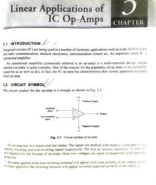
  • 1. Linear Applicationssof IC Op-Amps CHAPTER 3.1 INTRODUCTIOON Integrated circuits (IC) are being used in a number ofelectronicapplications such as in the field of audio and radio communication, medical electronics, instrumentation control ete. An important linear IC 1s operational amplifier. An operational amplifier (commonly referred to as op-amp) is a multi-terminal device whose internal circuitry is quite complex. One of the reasons for the popularity of op-amps is its versatility (used for ac as well as dc), in fact, the IC op-amp has characteristics that closely approach assumed ideal op-amp. 3.2 CIRcUIT SYMBOY The circuit symbol for the op-amp is a triangle as shown in Fig. 3.1. +V Positive Supply Inverting input -o Output Non-inverting o- input Negative Supply V Fig. 3.1 Circuit symbol of op-amp An op-amp has two inputs andoneoutput. The inputs are markedwith minus (-) and plus (+) tospecify inverting and non-inverting inputs respectively. The two dc sources, named as +V and -V are required for the biasing of op-amps, these two voltages are equal in magnitude with ôpposite polarities. n input applied at the non-inverting terminal will appear with same polarity at the output, while an input applied to the inverting terminal will appear inverted (opposite) polarity at the output. )
  • 2. 33 EQUIVALENT CIRCUIT MODEL ne equivalent circuit model ofan op-amp is shown in Fig. 3.b Inverting input U1 Ro wUdR Avd Non-inverting input V2 - Fig. 3.2 Equivalent circuit of op-amp The output section consists of a voltage controlled source in series with the output resistance R, It is evident from Fig. 3.2 that the input resistance R, is the Thevenin equivalent resistanceseen at the input terminal. The differential input voltage v, is given by ...(3.1) where v, = voltage between the inverting terminal and ground V =voltage between the noninvertingterminal and ground The op-amp senses the difference between the two inputs, multiplies it by the gain A, and causes the resulting voltage to appear at the output. Thus, the output v, is given by VAvd A(V2 V 3.2) Where 4 is called the open-loop voltage gain (it 1S also represented as A) because it is the gainof the op-amp without any feedback from output to input. /3.4 AN IDEAL OP-AMP An ideal op-amp is an amplifier with infinite open-loop gain, infinite input resistance and zero outputanee An op-amp is ideal ifit has the rollowing characteristics. Also given in the table are typical values of practical op-amps. Characteristics Ideal op-amp Practical op-ampP Open loop gain (A) 104 Open loop bandwidth (BW) =1MHz Input impedance (Z 210 2Output impedance (Z,) 500 2 (Contd)
  • 3. Linear pPp Characteristics Ideal op-amp Practical op-amp 70 dB Common Mode Rejection Ratio (CMRR) Input Offset voltage 0 < 10 mV Input Offset current 0 <20nA 3.4.1 Important Characteristics of an ldeal Op-amp For circuit analysis, an ideal op-amp is illustrated in Fig. 3.3. i0 + V2= 01 Fig. 3.3 ldeal op-amp model The important characteristics of an ideal op-amp are 1. The current into both input terminals are zero i0 and i,=0 ..(3.3) This is due to infiniteinputresistance. An infinite rsistance between the input terminals implies that an open circuit exists there and current cannot enter the op-amp . The difference voltage across the input terminals is negligibly small dV2V =0 Therefore, 1V2 ...(3.4) nus, an ideal op-amp has zero current into its two input terminals and negligibly small voltage between two input terminals. 3.4.2 ldeal Voltage Transfer Curve dge A transfer curve may be defined as a curve which is drawn between input and output ges.For op-amp the input voltage is v, and output is vo: A practical limitation of the op-amp 1s magnitude of its output voltage cannot exceed | Vcc or |VIIn other words, theoupl CS dependent and is limitedby the power supply voltage. Fig. 3.4 illustrates that the op-ampP Operate inthree modes, depending on the differential input voltage Va
  • 4. 3.9 VOLTAGE TO CURRENT CONVERTER OR V-I cONVERTER In a voltage to current converter, the output load cuTent is proportional to the input voltage. Accordingto the connection of load there are twotypes of V to / converters: Floating type and Ground type. In floating tvpe V to I converter R, 1s not connected to the ground whereas in grounded type. oneend of R, is connectedto the ground.
  • 5. 102 3.9.1 Voltage to Current Converter with Floating Load for ldeal Op-amn accepts anVoltage to current converter (V-I converter) is also called a transconductance amplifier. It accserter in input voltage v and produces an output current Fig. 5.15 shows a voltage to currentconvere which load resistor R, is floating. it is not connected to physical ground RL RL w - ww -io R ww. w R - iVin Voltage at these terminal must be same inirno current enter to the op-amp (b) Non-inverting configuration(a) Inverting configuration Fig. 3.15 V-I converter for an ideal op-a From Fig. 3.15(a) and (b) As input current of op-amp is zero. The output current i, can be written as Vin i R ..(3.30 i,Vin ..(3.31 Thus the load current is always proportional to the input voltage and circuit works as voltage current converter. The proportionality constant is generally 1/R,. Therefore, this circuit is also calle transconductance amplifier. It is also called a voltage controlled current source (VCKS). 3.9.2 Voltage to Current Converter with Grounded Load for ldeal Op-amp Figure 3.16 shows a voltage to current converter for ideal op-amp in which one end ofload resistor IS grounded. It is also known as "Howland current converter from to name of its inventor. The analysis of the circuit is accomplished by first determining the voltage v at the non-invertin input terminal and then establishing the relationship between v, and the load current. Apply KCL at node v, we get i+iiL in24 2 = isR R
  • 6. Linear Applications of IC Op-Amps inV 2v, = il Yn+YiR V .(3.32) 2 R R V1 w ww- Vo R V2 www- - i2R RL V Fig. 3.16 Voltage to current converter with grounded load R Rhe gain ofop-amp in non-inverting mode is given as A=1+ . for this circuit it is given as follows 33) A=1+ R 2 .(334)Hence output voltage can be written as 2 Substitute the equation (3.32) in equation (3.34) R -i, R
  • 7. 104 i R= Vn (3.35)Vin R From the equation (3.35) we can say that the load current depends on the input voltage v and resistor R. An the current to voltage converter, the output voltage is proportional to the 1nput current. It accepts an input current i, and produces an output voltage v,suchthatv =Ai, where A is the gain of the circuit. Figure 3. 17 shows the current to voltage converter. CURRENT TO VOoLTAGE cONVERTER OR -V CONVERTER R VoVa O Fig. 3.17 Current to voltage converter The nodea is an virtual ground as node b is grounded. .(3.36) R R ..(3.37)V R (3.38)o The gain A is measured in ohms, it is more appropriate to denote gain by symbol R. Because of this. I-V converters are also called ransresistance amplifiers. This circuit is also referred as current controlled voltage source (CCVS). If the resistance in crcUl is replaçed by the impedance, the cireuit is calicd transimpedance amplifier GENERALIZED IMPEDANCE CONVERTER (GIC) hpedance converters are active RC circuits designed to sinmulate frequency dependent elements suettas inductances for use in active filter synthesis. A simple general impedance converter (GlC) is show?in Fig. 3.18. It can be used not only to simulate inductances, but also to synthesize frequéney-dependentresistances.
  • 8. ZZsZ Z Fig. 3.18 Generalized impedance converter (GIC) Find the equivalent impedance seen looking nto node A. We apply a test voltage as shown n Fig. 3.19, we find the resulting current / and then Z - VI. Fach op-amp kecps (voltage at inverting and non-inverting terminal must be same), we ha labeled the voltages at the circuit nodes ofboth op-amps as By ohm's law we haNe 7 Summing currents at the node common to /, and,
  • 9. a Circuits 106 V2 V Z V2V1 Z V IIV v V1 Fig. 3.19 Finding equivalent impedance Summing currents at the node common to Z and Z V-V_ V-0 Z4 Z5 ..(3.41)VV0- =o ZsZ4 From equation (3.41) V2 ..(3.42) Y r 2 + Z From equation (3.39) V- V=1Z Substitute (V- V) in equation (3.40) -IZ1 =0 Z3 .(3.43)
  • 10. 107Linear Applications of IC Op-Amps Substituting V, from equation (3.42) in equation (3.43) V(Z +Z4)_ IZ Z325 Z Z Z+Z-Z Z,Zs The impedance Z is defined as Z==44ils ...(3.44) Z,Z4 Depending on the type of components we use for Z, through Z. We configure the circuit for various impedance types. 3.11.1 Simulation of Inductars Inthe generalized impedance converter, the Z, = Z, = Z, Zs = R and Z, is replaced by 1/sC as shown in Fig. 3.20. From Fig 3.20 Voltage at inverting and non-inverting terminal must be same, therefore, voltage at these terminal represents V (see the analysis step 1, 2, 3 in Fig. 3.20). Current entering into the op-amp is zero is identified in analysis steps 4, 5, 6 and 7 as shown in Fig. 3.20. Current through the capacitor is(as shown in analysis Step 8 of Fig. 3.20) Rs Voltage at V, is analysed in step 9 of Fig. 3.20. V2=V+ sC4 Rs Current through the resistor R is 2 (see the analysis Step 10 of Fig. 3.20) R3 V-V-- sC4 Rs= R3 sR,RC4
  • 11. 108 Number with circle represents analysis step. A2 R3 1 / s C V1 R2R www V2 R11) 40 1 Rsv A1 V1 Fig. 3.20 Inductance simulation circuit with analyzing steps Current through resistor R, is same as the current passing through resistor R2. In step 11, we determine the voltage V V= V- R2 sRR,C4 .The current through R, is determined as follows (see the analysis step 12 as shown in Fig. 3 VRV-V + sR,RC4 VRV-V= R R sRR3RC4 From step 12, the total current entering into the circuit of Fig. 3.20. VR ...3.4 sRR3R5CC4 The input impedance =-sRRzR,C_ sL R2 .(3.4 which is that of an inductance L given by L RR,C R2 .(3.4 ced Note: We obtain the similar inductance function when the impedance Z,, Zz, Z,Z are replaceby resistance and Z, = 1/sC, than the inductance becomes L= RRsC R
  • 12. Linear Applications of lC Op-Amps Filter is a frequency selective circuit that iscapable of passing signals with certain selected frequencies while rejects signals of all other frequencies. This property ofa filter is called frequency selectivity. Fig. 3.21 shows the classification of filters. 3.12 INTRODUCTION TO FILTERS Filter Digital filter Analog filter Passive filterActive filter Active RC filters Switched-capacitor filters. Fig. 3.21 Classification of filters Passive filters are constructed using inductors and capacitors, such filters work well at high frequencies.However, at low frequency the required inductors are large and physically bulky, and their characteristicsare quite non-ideal. Such inductors are impossible to fabricate in monolithic form and are incompatiblewith modern techniques. Active-RC filters employ op-amp with resistors and capacitors using discrete or hybrid thin-filmtechnology. Atthe present time, the most viable approach for real1zing full integrated monolithic filters isthe switched-capacitor technique. dvantages of active filters over passive filter are 1. The maximum gain or the maximum value of the transfer function may be greater than unity.2. The loading effect is minimum, which means that the output response ofthe filter is independentof the load driven by the fitter. 3. Due to flexibility in gain and frequency adjustments, the active filters can be easily tuned. 3.12.1 Limitation of Active Filters. The finite bandwidth of the active devices place a limit on the highest frequency of operation..The important factor oftheactive filter is sensitivity. The active elements are much more sensitiveto the temperature and the environmental changes than the passive elements. Hence due tochanges in the parameters due to the environmental changes, the active filter performance deviatesfrom its ideal response. Active filter require dc power supply to operate it but the passive filter do not require the desupply.
  • 13. OF SECOND ORDER FILTER3.15 GENERAL STRUCTURE An improved transmission characteristics (frequency response) can be obtained by using a second order active filter. A second order filter eonsists of two RC pairs and has a roll-off rate is -40 dB/decade. A general second order filter (Sallen-key filter) is shown in Fig. 3.34. R R www- w VA VB Y YVi A 1 Fig. 3.34 General structure of second order filter (Sallen-key model) The op-amp is connected in non-inverting amplifier and hence .(3.77) - A,VB where A is the closed loop gain. VB is the voltage at node B.
  • 14. 124 Apply KCL at node A is given .3. From equation(3.77), V andsubstitute v, in equation (3.78) Ap ..(3 vY Y + Y + Ap -v, Y Apply KCL at node B is given VAY2 gY + Y) AY2 (Y, +Y Y2+Ya A ( 3 Substituting equation (3.80) in equation (3.79) we get the voltage gain as v,Y,= ( +Y2 +73)- Ap -v,Y4, Y ( +YY +}, +¥)-Y¥2-4,Y,Y,| Y(+2+%)+Y,(+Y2 +Y)-Y2Y -4,Y,Y Ap2 +Yh +YY3 +Y4(K +Y2+Ys)-Y^Y'2 -ApY^Y|Vo ApY2
  • 15. YY +Y(Y% +Y2 +Y)+ Y,Y(1- 4,) .(3.81)T . Yy+ Ya(} + Y2 + Y) + Y2¥3(1 -4,) 3.15.1 Second Order Low Pass Filte Using Sallen-key model a second order low pass filter can be formed, if we set equal value of R and C for simplicity. Fig. 3.35 shows the second order low pass filter. Ri Ri ww www- R1 R2 OVo ww ww C CL Fig. 3.35 Second order low pass fiter From Fig. 3.35. Let we consider Y h=sC; and Y, =sC2 R R Substitute above values in equation (3.81) Ap R R T(s) +sC R R2 0-44)R R
  • 16. Integr 126 Ap (RR+R2+sRR2C + sRC(1 4,) RR21+sRRC2 Ap 14sC, (R + R,)+s2R,R,CC2+sR{C1 4p A,/R,R,CC2 s(RC2 + R,C2 +RCi(1-4,) RRCC2 1T(s) = RRCC2 Note: For simplicity we consider R, = R, = R and C, = C, = C the two equation (3.83) Ap 1+sC(2R)+s*R-C?+sRC(1=A,) Ts)= ApT 2R?c2+sRC(3-A,)+1 From equation (3.84) we conclude that ) For low frequencyf= 0 (s = 0) T(0)=Ap (i) For high frequency f= (s = oo T(oo)= 0 it shows that the frequency response is look like LPF.
  • 19. A band-pass filter passes all those frequencies lying with in a band between a lower-cut-off frequency (S) and a higher cut-off frequency (p) and rejects or attenuate all other frequencies outside this specified band. A generalized band pass response is shown in Fig. 3.41. 36 BAND PASS FILTERS Gain Ap 0.707 Ap f(Hz) fo f Fig. 3.41 Frequency response of band pass filter The difference betweenfy andff (>S) is the bandwidth of a band pass filter. As we know, the quality factor of any filter is measure of selectivity of that filter means the higher the value of . The band pass filter can be classified based on Q. 1. Narrow band pass filter (> 10) 2. Wide band pass filter (10) The quality factor of a band pass filter is the ratio of centre frequency () to the bandwidth (BW) Jo= - BW 4i u o ...(3.104) where bandwidth BW=Iu-J The centre frequency fo- NSHfL .(3.105) The quality factor (O) can also be expressed in terms of damping coefficient of a filter Ste .(3.106)
  • 20. 3.16.1 Structure ofBand pass Filter A band pass filter can be formed by cascading high pass and low pass filter as shown in Fig. 3.42. Th cut-off frequency or corner frequency of high pass filter (/) must be higher than corner frequenc) f) of low pass filter. High pass filter (f) Low paSS filter (fH) VoutVi High-pass Low pass sectionsection Fig. 3.42 Structure of band pass filter
  • 21. 3.17 BAND STOP FILTER Band stop filter or band elimination filters stops the frequencies in the stop band and pass all other frequencies outside the stop-band Types of Band stop filter 1. Wide band stop filter (< 10) 2. Narrow band stop filter (Q> 10) or notch filter The O ofthe narrow band stop filter is high and they are known as the notch filter. Due to large value of O, the bandwidth of band stop filter is smaller than that of the wide band stop filter 3.17.1 Wide Band-Stop Filter Figure 3.47 shows the block diagram of wide band-stop filter and it consist of a low pass filter, a high pass filter and summing amplifier. In order to practically obtain the frequency of a wide band stop filter, we have to adjust the cut-off irequencyf, of high pass filter is higher than the cut-off frequencyf 0f low pass filter.
  • 22. ..(3.128)For band stop filter wide band stop filter response L Highpass filter H fL Summing amplifier Vo Vin fHfLLowpass filter Fig. 3.47 Block diagram of wide band-stop filter Fig. 3.48 shows the wide band-stop filter using three op-amp RF High pass filterR1 R4R2 ww www Summing amplifier C R R3 o Vout RR 2 RoM C A2 Low pass filterw R'F R1 Fig. 3.48 Wide band-stop filter
  • 23. The combined frequency response ofis shown in Fig. 3.49. Another important constraint is that the passband of the lowpass and high pass filters should be identical. The centre frequency is given by ...(3.129) Gain Pass band Stop band Pass band f cut-offfrequency of HPF G fH Cut-offfrequency of LPF 0.707 G Frequency response of LPF fH fo L Frequency response of HPF Fig. 3.49 Frequency response of wide band-stop filter
  • 24. 3.19 ALL PASS FILTR But The filters which are discussedlused to adjust the magnitude ofthe transfer functionof thecircul nis also alters the phase angle characteristics of the circuit. It is many times required to cOnuo phase response of the filter. The filter which is used to control the phase response by adding a phase shift between input and Output signals is called as all pass filter. Its gain is one for all thefrequencies.
  • 25. Thus, as the name suggests, it passes all the frequencies of the input Signal. It does not procduoe attenuation but provide the required phase shift for the different frequencies ofthe input signal. Fio 3 shows the simple first order all pass filter. ice:any signal.Fig.3. 158 R= R1 R B o Vo V O A ww- R Fig. 3.52 All pass filter Analysis of the Circuit Let us use the superposition principle to obtain the expression for the output voltage v,. Fig. 3.53(a) and (6) shows the circuit with consideration ofone input connected to input and other input is made ground. Assume input to the non-inverting terminal zero as shown in Fig. 3.53(a). The circuit acts as an invertingamplifier R RR wwR R1 O Vo2 R VAViO ww ViO- ww Vo 1/sC (a) (b) Fig.3.53 R -VË R Vol Vol-V when R-R ...(3.132)