CCS355 Neural Networks & Deep Learning Unit 1 PDF notes with Question bank .pdf
Gas sensor
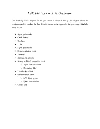
1. ASIC interface circuit for Gas Sensor:
The interfacing block diagram for the gas sensor is shown in the fig. the diagram shows the
blocks required to interface the data from the sensor to the system for the processing. It includes
many blocks
Signal path blocks
Clock divider
Band gap
LDO
Signal path blocks
Sensor excitation circuit
Front end
Dechopping network
Analog to Digital conversion circuit
o Sigma delta Modulator
o Decimation filter
Linearization circuit
serial Interface circuit
o i)I2C Slave module
o ii)SPI Slave module
Control unit
2. Fig 1: Block diagram of gas Sensor interface ASIC circuit
1. Signal Path Blocks:
The MEMS sensor is excited by a chopped supply signal. The differential voltage measured
across the sensor is amplified by the Front End to a level that is compatible with the ADC. The
differential output is dechopped after amplification. Sigma-Delta ADC was used because of its
low power and high resolution needed with low bandwidth, which is suitable for the slow
mechanical nature of the gas flow. The Sigma-Delta Modulator converts the dechopped
amplified output into an oversampled single bit stream with noise shaping. The quantization
noise added to signal is lowered in the band of interest but most of its power exists in the out-of-
band high frequencies. A Decimation Filter then is implemented to attenuate the out-of-band
noise, which can be aliased back into the base band, and down-sample the bit stream into a
sampling frequency that is comparable to the Nyquist one with higher word-length for each
sample. Linearization Block takes place to compensate the sensors non-linearity. After obtaining
the correct flow rate, the Serial Interface Unit sends this data to the user via SPI or I2C serial
connection. The user can choose the rate of readings acquisition. The chip can operate on two
modes. The user can choose the Continuous Mode of operation to power ON the chip and
receive the recent readings continuously with maximum output data rate. On-Demand Mode
3. enables user to power ON the chip to capture the current flow rate. The Control Unit will then
turn OFF the chip again to reduce power consumption until a new request is sent by the user. The
user can receive the last registered reading as long as no new request is sent.
2. Auxiliary Blocks:
The Band Gap supplies accurate voltage references to the ADC, the Common-Mode Feed- back
(CMFB) reference, and the sensor excitation voltages. Chopping technique is used in the Band
Gap OTA. Low noise output buffer is implemented to satisfy the SNR. Voltage to current
converter generates DC current to bias the different Op-Amps in the system. The LDO supplies
the digital domain transistors with the 1.2V VDD. Clock Divider is responsible for generating
different clocks with different frequencies and phases to feed the digital, ADC, chopper and de-
chopper using the reference clock of the external oscillator.
3. Front-End Circuit:
It is an instrumentation amplifier with trimming resistors. The process variations in fabrication
result in sensor resistors mismatch. Trimming resistors are used to compensate this mismatch. A
bank of series resistors, each in parallel with a switch controlled by a Control Bit (CB), is used
for trimming.
Fig 2: Instrumentation amplifier with trimming resistors
4. And then amplifies the sensor chopped signal. This circuit can be implemented by writing the
Verilog AMS front end code and simulated with the Xilinx tools for the verification of the sensor
signals.
electrical cout;
real Vin_real;
real C1,gm,R1;
parameter real Vos=0;
parameter real Rin=1M;
parameter real Rout=100;
param
eter real gain=1.0e5;
parameter real GBW=1.0e8;
parameter real iin_max=100e-
6;
parameter real slew_rate=0.5e6;
parameter real ibias=100e-
6;
analog begin
@(initial_step)
begin
C1=iin_max/slew_rate;
gm=2*`M_PI*freq_unitygain
*C1;
R1=gain/gm;
End
I(inn)<+ibias;
I(inp)<+ibias;
Vin_real=V(inp,inn)+Vos;
I(inp,inn)<+Vin_real/Rin;
I(cout)<+
-gm*Vin_real;
I(cout)<+C1*ddt(V(cout));
I(cout)<+V(cout)/R1;
I(out)<+
-V(cout)/Rout;
I(out)<+V(o
ut)/Rout;
end
//Verilog
-AMS HDL for
"thc_UIRFPA_AMS_10DEC20", "integrator"
"verilogams"
5. `include "constants.vams"
`include "disciplines.vams"
module integrator (out,level,in);
output out;
input in,level;
electrical out,in
; disciplines
logic level;
integer assert;
parameter real ic=0;
parameter real gain=
-1e9;
parameter real reference=2.4;
analog begin
if(level)
begin
assert=1;
end
else
begin
assert=0;
end
V(out)<+gain*idt((V(in)
-
reference),ic,assert)+reference;
end
endmodule
2. Chopping Network:
Slow mechanical nature of the gas flow causes the system to suffer from the low-frequency
flicker noise. Chopping the signal improved the overall system signal-to-noise ratio (SNR)
significantly as the effect of flicker diminished. Chopping was made by flipping the bias of the
sensor with frequency of 5 kHz, then after amplification, the signal was de-chopped by double
balanced mixer [4] to minimize losses. Double mixer can be implemented and simulated using
Verilog A and Xilinx.
6. Fig 3 : Double balanced Mixer
3. Analog to Digital Circuit:
The amplified sensor signal from the Dechopper can be digitalized using a low-power high-
resolution Sigma-Delta ADC. Analog to Digital converter has a Sigma-Delta modulator and a
decimation filter. Circuit level implementation of the second order Sigma-Delta Modulator is
shown in the fig.
Fig 4 : Second order ∑∆ Modulator with decimation filter
It is composed of two integrators, comparator and 1-bit DAC feedback, with the specifications
Bandwidth 250Hz, sampling frequency 256 kHz, quantization bits-1 and Figure of merit 27.9
fJ/conv. In order to fulfill the gain error requirements, telescopic OTA, was used with gain of 89
dB, phase margin of 70◦, and with common mode voltage of 1.5 volt. Averaging resistances
used for CMFB circuit,[9] , in order to maintain the CM level at the required value.
7. Fig 5 : Telescopic OTA
Decimation Filter: Decimation is implemented using the multiplier-less CIC filter. Additional
low-pass filtering is done using the IIR Elliptic low-pass filter to increase the SNR, Fig. 8, in
whole spectrum by attenuating the out-of- band noise power. The phase linearity is not required
due to the application nature.
Fig 6 : ADC with Decimation block
The comb-half-band FIR-FIR decimation filter is designed using Matlab and checked for real-
time implementation using Simulink. The decimation filter is designed for 6-bit data stream
input. The final output of the filter is 13 bits, and the stop band attenuation obtained is-65 dB. In
addition, the distributed arithmetic multiplier is used for implementing in VHDL. Specifically,
we compare the relative power consumption of two designs; the cell usage for each design is
8. obtained using the synthesis report. The proposed decimation filter architecture requires less
hardware and contributes to a hard ware saving compared to the comb -FIR-FIR architecture.
4. Linearization circuit:
Generally the sensor’s output signal is in the form of non-linear, the signal can be brought to
linear form with the help of Linearization circuit. When the signal is in the digital domain
achieving linearization is easy. The inverse relation between the sensor signal and the flow rate is
implemented using a combinational logic. An eight-segment piece-wise linear fitting is
performed. The block input is multiplied by a constant coefficient. This multiplication is
converted into a number of shifted versions of the input to avoid using multipliers that consume
high area and power. The total maximum relative error due to fitting and quantization is 0.65%
of the full-scale.
5. Control Unit:
The Control Unit turns ON and OFF the analog blocks, the decimation filter, and the
linearization block according to the interface bus state and mode of operation determined by the
external processor or micro-controller, i.e., the user.
Continuous Mode: The master initiates the connection by sending an all-zeroes word using SPI
or I2C. The chip will respond by an Acknowledgment all-ones word to the master request till the
first reading is ready. Using SPI communication, the user can then receive the samples
continuously.
On Demand Mode: The master initiates the connection by sending an all-ones word. The chip
acknowledges till the reading is ready, buffers it and turns OFF again. The user can receive the
last buffered reading using SPI or I2C unless no new request is sent.
6. Serial interface Unit:
The Serial Interface Unit is always ON to detect the connection and send status signals to the
Control Unit and then receive commands. Slave modules for SPI and I2C are implemented
inside. After RESET, it turns ON both modules to detect which communication standard is used.
Then, it turns OFF the unused module.
The linearized gas sensor Standard serial communication protocols, SPI and I2C, are supported
to interface with the system. The chip supports two modes of operation. It can operate
continuously for maximum output data rate. In addition, the system ON period can be controlled
using the on-demand mode to lower the power consumption. Implementation of the complete
1) SPI Module: This module is adjusted for fixed word length (15 bits), CPHA=0 and CPOL=0.
9. 2) I2C Module: It operates at the standard mode with 7- bit addressing scheme. Clock stretching
is not supported. The chip address is hardwired. The most significant byte is sent first.
Test
1
coverage
Scoreboard
Multi-channel
controller
Programs
theI2C
and
transfers
traffic
BUS
Verificatio
n
Compone
nt
I2C DUT
Bus
interface
Control/Interru
pt
Logic
Slav
e
buffe
r
Maste
r
buffer
Control/Stat
us
Registers
I2C
Verificatio
n
Compone
nt
Controls BUS
and
I2C
components
Test
2
Test
3
Tests
indicate
which
stimulus
sequences
to execute
BUS
Seri
al
10. The aim is to develop I2C Verification IP using open verification methodology to verify I2C
module. The I2C (Inter-IC) bus is a bi-directional two-wire serial bus that provides a
communication link between integrated circuits (ICs). There are three data transfer speeds for the
I2C bus: standard, fast-mode, and high-speed mode. Standard is 100 Kbps. Fast-mode is 400
Kbps, and high-speed mode supports speeds up to 3.4 Mbps.
ASIC system for interfacing gas sensor can be implemented and layout using a CMOS 90nm
technology. The entire interfacing circuit can be implemented in Verilog /Verilog-A/ Verilog
ASM HDL. The implementation is tested on Spartan FPGA board. Finally ASIC chip can be
fabricated with the 90nm/45nm CMOS technology in association of Semiconductor Labs,
Chandigarh.
For ASIC implementation the requirements
System Verilog soft ware
Questa Simulator
Spartan FPGA Board
Fabrication Facilities