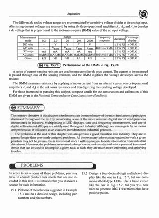
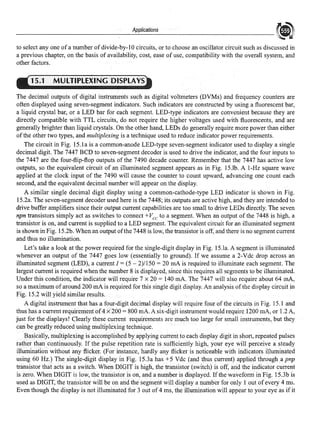
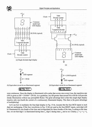
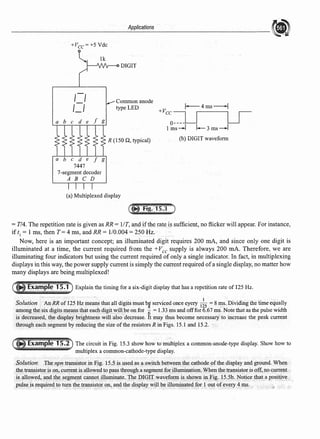
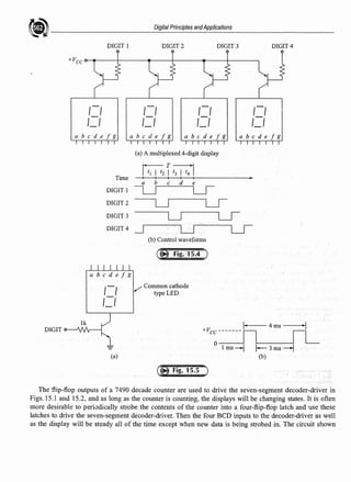
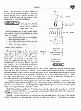
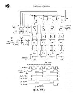
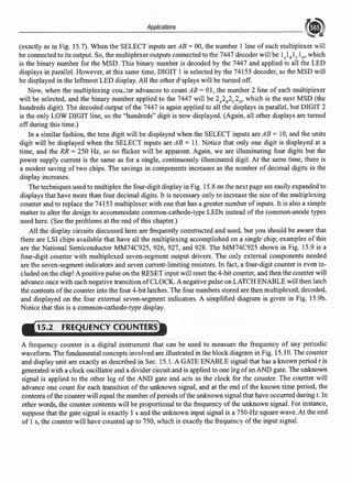
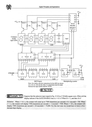
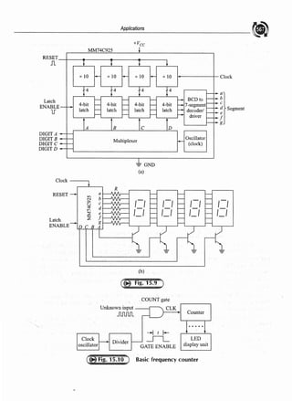
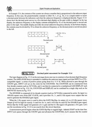
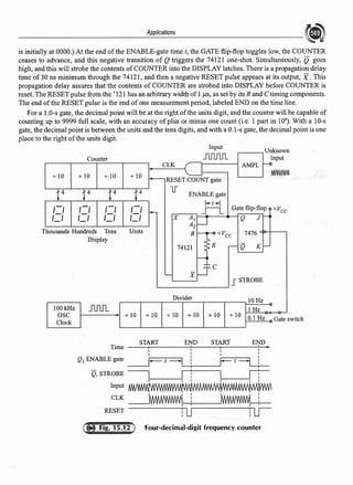
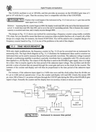
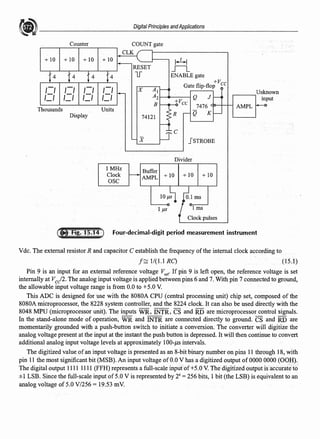
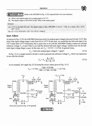
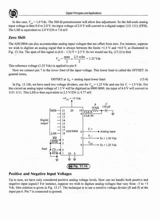
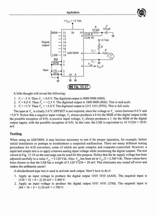
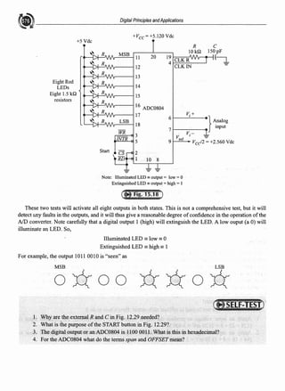
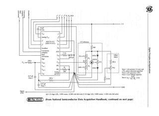
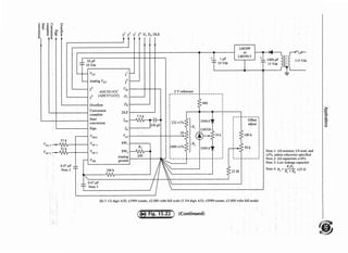
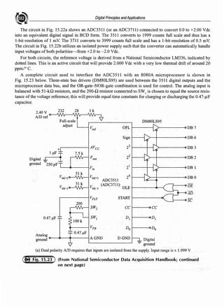
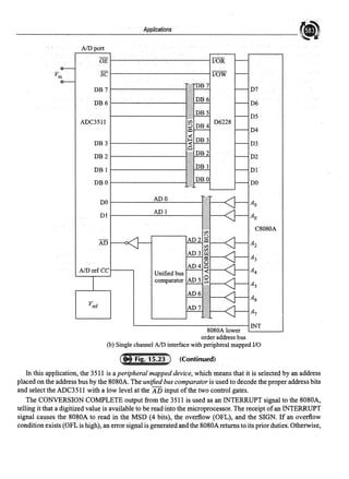
This document discusses applications of digital circuits, including multiplexing LED displays, frequency counters, time measurement circuits, and analog-to-digital converters. It focuses on multiplexing techniques to reduce power requirements for LED displays. Multiplexing works by pulsing each display digit sequentially rather than illuminating all digits continuously. With a high enough pulse repetition rate, the eye perceives steady illumination without flicker. The document provides examples of multiplexing common anode and common cathode LED displays, and discusses methods for generating control waveforms. It also covers applications using AD converters like the ADC0804 and ADC3511 to build instruments like digital voltmeters.
FREQUENCY COUNTERS AND TIME-INTERVAL MEASUREMENTS.pdfssuser72979d
This document discusses frequency counters and time-interval measurements. It begins by explaining how frequency counters operate by gating an input frequency signal into a counter for a precise time period, such as 1 second, to directly measure the average frequency in Hertz. The core of most frequency counters is a cascade of binary coded decimal counters interfaced with a seven-segment display. Frequency counters revolutionized precise frequency measurement by replacing older analog techniques with digital logic and fast counting.
The document describes a digital alarm clock circuit designed using the TMS8560 integrated circuit.
The circuit includes components like the TMS8560 and CD4541B ICs, a 3.2768MHz crystal oscillator, 7-segment displays, transistors, resistors, capacitors, and buttons to set the time and alarm. The TMS8560 IC drives the display and generates the alarm signal, while the CD4541B is used as a timer to swap between alarm sounds. The circuit works by allowing the user to set the time and alarm via buttons, which is then driven to the 7-segment display. The alarm signal is amplified to power a buzzer or speaker. Troubleshooting focuses on
This document discusses various applications of embedded systems including temperature measurement using thermistors and linear temperature sensors like the LM35. It describes how to interface the LM35 temperature sensor with an 8-bit ADC0809 and microcontroller port for temperature readings. It also discusses controlling a stepper motor and interfacing it to port pins of a microcontroller. Finally, it explains interfacing a 2x16 LCD display and keyboard matrix to a microcontroller for input/output applications.
The document describes the design of a digital stopwatch circuit using integrated circuits. The circuit uses a pulse generator to create a 1Hz clock signal, a counter integrated circuit to count the pulses and track seconds and decades, and display driver integrated circuits to show the time on 7-segment displays. With minor modifications, the circuit could be adapted for applications like photo counting, people counting, timers, and alarms. Building the circuit provided learning experiences in pulse generation, troubleshooting circuits, using displays and drivers, and soldering circuits on PCBs.
Analog to Digitalconvertor for Blood-Glucose Monitoringcsijjournal
ABSTRACT
This paper presents the design of a low-power CMOS current-frequency (I–F) Analog–Digital Converter. The ADC is designed for implantable blood-glucose monitoring. This current frequency ADC uses nArange of input currents to set and compare voltage oscillations against a self-produced reference to resolve 0–32nA with an accuracy of 5-bits at a 225MHz sampling rate. The comparator used is a dynamic latch comparator and the output is fetched from a 5-bit counter. This is designed in 180nm CMOS technology with a supply of 1.8V, it operating voltage taken here is 0.0- 1.8V with power consumption of 12.3nW using Cadence tools.
ANALOG TO DIGITALCONVERTOR FOR BLOOD-GLUCOSE MONITORING csijjournal
This paper presents the design of a low-power CMOS current-frequency (I–F) Analog–Digital Converter. The ADC is designed for implantable blood-glucose monitoring. This current frequency ADC uses nArange of input currents to set and compare voltage oscillations against a self-produced reference to resolve 0–32nA with an accuracy of 5-bits at a 225MHz sampling rate. The comparator used is a dynamic latch comparator and the output is fetched from a 5-bit counter. This is designed in 180nm CMOS technology with a supply of 1.8V, it operating voltage taken here is 0.0- 1.8V with power consumption of 12.3nW using Cadence tools.
Construction of digital voltmeter by Bapi Kumar DasB.k. Das
The document describes the construction of a digital voltmeter. It discusses 6 main sections: 1) a pulse train generator, 2) control and gating circuitry, 3) a counting section, 4) an analog input/transducer, 5) a latching and display section, and 6) completing the connections between all sections. The pulse train generator and control/gating circuitry work together to start and stop counting pulses based on the input voltage. The counting section then counts these pulses. The analog input converts the measured voltage to a signal. This signal is then latched and displayed on the digital readout.
This document is a lab manual for analog and digital circuits experiments in the third semester of an electronics and communication engineering program. It contains 15 experiments, including experiments on common emitter, common collector, common source, Darlington, and differential amplifiers as well as various digital logic circuits like code converters, adders, multiplexers, and counters. For each analog experiment, the document provides the aim, apparatus required, circuit diagram, theoretical background, experimental procedure and expected results. It also contains an index listing the experiments and corresponding page numbers.
Digital voltmeter using 89c51 microcontrollerSaylee joshi
Voltmeter is a voltage measuring instrument.
We can measure the potential difference between any two points in an electrical network using voltmeter.
There are two types of voltmeter as analog voltmeter and digital voltmeter.
Analog voltmeter moves pointer on a scale but it has some limitations like accuracy of few percent of full scale.
Digital voltmeter can display numerical value of voltage on a display by use of analog to digital converter (ADC).
All the data processing and manipulating is in digital form, so it is very essential to use ADC.
We have used ADC0804 analog-to-digital converter IC. The range of input voltage is 0-15V. Here the input voltage should be DC voltage so as to get the steady output on the LCD display.
If you give the AC voltage as an input, it will display continuously running numbers as the nature of AC voltage.
final Year Projects, Final Year Projects in Chennai, Software Projects, Embedded Projects, Microcontrollers Projects, DSP Projects, VLSI Projects, Matlab Projects, Java Projects, .NET Projects, IEEE Projects, IEEE 2009 Projects, IEEE 2009 Projects, Software, IEEE 2009 Projects, Embedded, Software IEEE 2009 Projects, Embedded IEEE 2009 Projects, Final Year Project Titles, Final Year Project Reports, Final Year Project Review, Robotics Projects, Mechanical Projects, Electrical Projects, Power Electronics Projects, Power System Projects, Model Projects, Java Projects, J2EE Projects, Engineering Projects, Student Projects, Engineering College Projects, MCA Projects, BE Projects, BTech Projects, ME Projects, MTech Projects, Wireless Networks Projects, Network Security Projects, Networking Projects, final year projects, ieee projects, student projects, college projects, ieee projects in chennai, java projects, software ieee projects, embedded ieee projects, "ieee2009projects", "final year projects", "ieee projects", "Engineering Projects", "Final Year Projects in Chennai", "Final year Projects at Chennai", Java Projects, ASP.NET Projects, VB.NET Projects, C# Projects, Visual C++ Projects, Matlab Projects, NS2 Projects, C Projects, Microcontroller Projects, ATMEL Projects, PIC Projects, ARM Projects, DSP Projects, VLSI Projects, FPGA Projects, CPLD Projects, Power Electronics Projects, Electrical Projects, Robotics Projects, Solor Projects, MEMS Projects, J2EE Projects, J2ME Projects, AJAX Projects, Structs Projects, EJB Projects, Real Time Projects, Live Projects, Student Projects, Engineering Projects, MCA Projects, MBA Projects, College Projects, BE Projects, BTech Projects, ME Projects, MTech Projects, M.Sc Projects, Final Year Java Projects, Final Year ASP.NET Projects, Final Year VB.NET Projects, Final Year C# Projects, Final Year Visual C++ Projects, Final Year Matlab Projects, Final Year NS2 Projects, Final Year C Projects, Final Year Microcontroller Projects, Final Year ATMEL Projects, Final Year PIC Projects, Final Year ARM Projects, Final Year DSP Projects, Final Year VLSI Projects, Final Year FPGA Projects, Final Year CPLD Projects, Final Year Power Electronics Projects, Final Year Electrical Projects, Final Year Robotics Projects, Final Year Solor Projects, Final Year MEMS Projects, Final Year J2EE Projects, Final Year J2ME Projects, Final Year AJAX Projects, Final Year Structs Projects, Final Year EJB Projects, Final Year Real Time Projects, Final Year Live Projects, Final Year Student Projects, Final Year Engineering Projects, Final Year MCA Projects, Final Year MBA Projects, Final Year College Projects, Final Year BE Projects, Final Year BTech Projects, Final Year ME Projects, Final Year MTech Projects, Final Year M.Sc Projects, IEEE Java Projects, ASP.NET Projects, VB.NET Projects, C# Projects, Visual C++ Projects, Matlab Projects, NS2 Projects, C Projects, Microcontroller Projects, ATMEL Projects, PIC Projects, ARM Projects, DSP Projects, VLSI Projects, FPGA Projects, CPLD Projects, Power Electronics Projects, Electrical Projects, Robotics Projects, Solor Projects, MEMS Projects, J2EE Projects, J2ME Projects, AJAX Projects, Structs Projects, EJB Projects, Real Time Projects, Live Projects, Student Projects, Engineering Projects, MCA Projects, MBA Projects, College Projects, BE Projects, BTech Projects, ME Projects, MTech Projects, M.Sc Projects, IEEE 2009 Java Projects, IEEE 2009 ASP.NET Projects, IEEE 2009 VB.NET Projects, IEEE 2009 C# Projects, IEEE 2009 Visual C++ Projects, IEEE 2009 Matlab Projects, IEEE 2009 NS2 Projects, IEEE 2009 C Projects, IEEE 2009 Microcontroller Projects, IEEE 2009 ATMEL Projects, IEEE 2009 PIC Projects, IEEE 2009 ARM Projects, IEEE 2009 DSP Projects, IEEE 2009 VLSI Projects, IEEE 2009 FPGA Projects, IEEE 2009 CPLD Projects, IEEE 2009 Power Electronics Projects, IEEE 2009 Electrical Projects, IEEE 2009 Robotics Projects, IEEE 2009 Solor Projects, IEEE 2009 MEMS Projects, IEEE 2009 J2EE P
This document describes the design of a digital voltmeter using an 8051 microcontroller and ADC0804 analog-to-digital converter. It includes the circuit diagram and explanations of the main components. The 8051 microcontroller reads the analog input voltage, converts it to a digital value using the successive approximation ADC0804, and displays the reading on an LCD screen. The document provides details on interfacing the ADC0804 and LCD, as well as the pin descriptions and timing diagrams for programming and operation. It aims to explain how to build a digital voltmeter circuit using low-cost microcontroller and ADC components.
DIGITAL VOLTMETER USING 8051 MICROCONTROLLERChirag Lakhani
This document describes the design of a digital voltmeter using an 8051 microcontroller. It includes the following key points:
- An analog to digital converter (ADC0804) is used to convert an analog input voltage to a digital signal that can be read by the microcontroller.
- The 8051 microcontroller then processes the digital signal from the ADC and displays the voltage reading on a liquid crystal display (LCD).
- The circuit diagram shows how the ADC, microcontroller, and LCD are interconnected. Key components include ports for input/output, a crystal oscillator, and voltage regulators.
- The document provides details on the pin configurations and functions of the 8051 microcontroller and ADC0804
This document discusses interfacing an analog-to-digital converter (ADC) and digital-to-analog converter (DAC) with an 8051 microcontroller. It describes the ADC0804 and DAC0808 integrated circuits. The ADC0804 is an 8-bit ADC that converts analog voltages to 8-bit digital values. It has a resolution of 8-bits and a maximum conversion time of 110us. The DAC0808 is an 8-bit DAC that converts digital values to an analog current. Software is provided to generate a sine wave using the DAC and control a stepper motor by interfacing it with the microcontroller ports. Programs in C are given to read the switch status and rotate
This document discusses various topics related to embedded systems including microcontrollers versus microprocessors, interfacing components like LEDs and LCDs, programming concepts like for loops and if statements, and examples of embedded systems like a digital clock and temperature sensor. It provides code examples in C programming language to interface different components and displays output screenshots.
UNIT 4 & 5 - I nterfacing_Lecture7.pptxnaveen088888
The document discusses analog sensor interfacing and analog to digital conversion. It explains that physical quantities in the real world are analog while computers use digital values, so an analog to digital converter (ADC) is used to convert analog sensor signals to digital values. It then describes the characteristics of ADCs like resolution, conversion time, reference voltage, and output data format. It provides examples of calculating the step size and digital output for different resolutions and reference voltages. Finally, it discusses different types of sensors, interfacing techniques for sensors, displays, and relays with microcontrollers.
This document discusses analog to digital conversion and pulse width modulation.
It explains that analog signals from peripherals must be converted to digital signals the microcontroller can understand using an analog to digital converter (ADC). It also describes how pulse width modulation varies the duty cycle of a signal to control motor speed or other analog systems. Common applications like temperature measurement and motor control are provided as examples.
The document discusses different types of analog to digital converters (ADCs). It describes 6 main types - counter/ramp ADC, tracking ADC, successive approximation ADC, flash ADC, delta-sigma ADC, and dual slope integrating ADC. For each type it provides a brief overview of the operating principle and block diagram. It also discusses important ADC specifications and parameters such as resolution, quantization error, dynamic range, signal to noise ratio, aperture delay etc.
1. Analog to digital converters (ADCs) sample analog signals and convert them into digital words. This allows analog signals from sensors to be processed digitally.
2. The conversion process has two steps - quantization breaks down the analog value into discrete levels, and encoding assigns a digital code to each level. For example, a 3-bit ADC of a 0-10V signal quantizes it into 8 levels separated by 1.25V and encodes each with a 3-bit binary code.
3. There are several types of ADCs including flash, successive approximation, delta-sigma, and dual slope. Flash ADCs are fastest but most expensive, while successive approximation and dual slope ADCs are slower
This document provides a summary of a progress report on the design of a 3-bit flash analog-to-digital converter (ADC). It describes the architecture and design of a comparator, which acts as a 1-bit ADC, and a 3-bit flash ADC. It also discusses characterization of the ADC's DC performance by measuring differential nonlinearity and integral nonlinearity from histograms. The document covers comparator design techniques, reference voltage generation using diode-connected transistors, and layout of the 3-bit flash ADC.
Parallel/flash ADCs use a voltage ladder and comparators to convert an analog input to a thermometer code. They can achieve sampling rates over 1GHz but require 2N-1 comparators. Interpolating and averaging ADCs reduce comparator count by interpolating between ladder voltages and averaging comparator outputs. Folding ADCs further reduce comparator count by mapping the input range onto a smaller set of subranges. Time-interleaved ADCs achieve high speeds by parallelizing conversions across multiple ADCs.
This document describes Leonard Kibet Ng'eno's diploma project presented in September 2013 at Eldoret Polytechnic College. The project is a simple digital security system using sensing loops to detect intruders. It has a signal input block, signal decoder block, visual display unit, signal encoder block, signal amplification block, and audio output block. The circuit works off a 9V power supply and uses common components like the 4511 7-segment decoder, transistors, resistors, and a piezobuzzer.
This document provides information about analog to digital conversion and digital to analog conversion. It discusses different types of converters including flash ADCs, successive approximation ADCs, dual slope ADCs, R-2R ladder DACs, and weighted resistor DACs. It also covers analog and digital signals, the conversion processes, and applications of ADCs and DACs in areas like data acquisition and fiber optic communication.
The document describes a 4-phase power supply design using the LTC3875 controller that can deliver 120A of current in a small footprint. It utilizes two LTC3875 controllers operating with 90 degree phase shifts to reduce ripple. Each phase supports 30A using a single top and bottom MOSFET. The LTC3875 can accurately sense currents even with inductors having very low DCR values as low as 0.2mOhms. The design achieves 87.1% efficiency at 120A output. An alternative design is presented using one LTC3875 controller and one LTC3874 slave controller to reduce component count and solution size.
This document provides an overview of testing techniques for analog-to-digital converters (ADCs) and discusses various types of moderate-speed ADCs. It describes common tests for measuring ADC performance including input-output tests, FFT tests, histogram tests, and sinusoidal input tests. Different ADC architectures are introduced such as serial ADCs, successive approximation ADCs, and pipeline ADCs. Specific circuit implementations and operating principles are outlined for single-slope, dual-slope, and successive approximation ADCs.
This document describes a 10-bit 165MSPS video ADC. It uses a time-interleaved SAR architecture with multiple low-power SAR ADCs operating in parallel to achieve the high sampling rate. Each SAR ADC samples every nth cycle, resulting in an effective sampling rate that is n times higher than an individual ADC. The design achieves low power consumption and area through its digital nature and use of scaled CMOS technology. It provides offset correction through a calibration technique to improve accuracy for video applications.
Complete solution for Recurrent neural network.pptxArunKumar674066
Recurrent neural networks (RNNs) are useful for processing sequential data like text or time series data. RNNs can remember previous inputs/outputs through their internal memory state, allowing them to find patterns in sequential data. However, standard RNNs struggle with long-term dependencies due to the vanishing gradient problem. Newer models like LSTMs and GRUs address this with gating mechanisms that allow them to better learn from early events in long sequences. RNNs are commonly used for natural language processing tasks like text generation and machine translation.
The document discusses combinational logic circuits and Karnaugh maps. It covers standard Boolean representation forms such as SOP and POS, conversion between forms, and realization using NAND/NOR gates. It also discusses minimizing Boolean functions up to 4 variables using Karnaugh map reduction techniques and designing arithmetic circuits and code converters using K-maps.
This document provides an overview of digital electronics. It discusses basics such as how computers understand binary digits. It also covers analog versus digital, advantages of digital like ease of design and speed. Applications of digital electronics include computers, mobile phones, and appliances like washing machines and refrigerators.
The document discusses the components of a communication system and their functions. It describes a communication system as having a source that produces a message, a transmitter that encodes the message into a signal, a channel that carries the signal between transmitter and receiver, and a receiver that decodes the signal back into a message. It also notes communication systems are subject to distortion during signal transmission and noise interference. The document provides a model of a basic communication system and explains the roles of key components like the transducer, transmitter, channel, and receiver.
Digital communication systems use digital modulation techniques to convert analog messages into digital signals for transmission. The three main digital band-pass modulation techniques are amplitude-shift keying (ASK), phase-shift keying (PSK), and frequency-shift keying (FSK). These techniques modulate a carrier signal by varying the amplitude, phase, or frequency according to the digital message. Receivers can use coherent or noncoherent detection, with coherent detection providing better performance but requiring synchronization to the transmitter carrier phase. The bandwidth requirement and transmitted energy depend on modulation parameters like the bit duration and carrier frequency.
The document discusses analog communication systems and amplitude modulation. It introduces key concepts such as elements of a communication system including the information source, transmitter, channel, and receiver. It describes amplitude modulation where the amplitude of a carrier wave is varied in accordance with the modulating signal. Common modulation techniques like DSB-SC and generation methods like using a square law or switching modulator are summarized. Detection or demodulation of the AM signal using detectors like square law, envelope, and rectifier are also outlined.
Gerd Keiser - Optical Fiber Communications-McGraw-Hill Education (2010).pdfArunKumar674066
This document provides an overview of the fourth edition of the textbook "Optical Fiber Communications" by Gerd Keiser. It discusses key topics covered in the book such as optical fiber structures and waveguiding, attenuation and dispersion, optical sources, photodetectors, digital and analog links, and optical networks. The book is published by McGraw-Hill and copyrighted in 2011. It is intended to provide comprehensive coverage of optical fiber communication systems and their components.
Understanding Inductive Bias in Machine LearningSUTEJAS
This presentation explores the concept of inductive bias in machine learning. It explains how algorithms come with built-in assumptions and preferences that guide the learning process. You'll learn about the different types of inductive bias and how they can impact the performance and generalizability of machine learning models.
The presentation also covers the positive and negative aspects of inductive bias, along with strategies for mitigating potential drawbacks. We'll explore examples of how bias manifests in algorithms like neural networks and decision trees.
By understanding inductive bias, you can gain valuable insights into how machine learning models work and make informed decisions when building and deploying them.
Presentation of IEEE Slovenia CIS (Computational Intelligence Society) Chapte...University of Maribor
Slides from talk presenting:
Aleš Zamuda: Presentation of IEEE Slovenia CIS (Computational Intelligence Society) Chapter and Networking.
Presentation at IcETRAN 2024 session:
"Inter-Society Networking Panel GRSS/MTT-S/CIS
Panel Session: Promoting Connection and Cooperation"
IEEE Slovenia GRSS
IEEE Serbia and Montenegro MTT-S
IEEE Slovenia CIS
11TH INTERNATIONAL CONFERENCE ON ELECTRICAL, ELECTRONIC AND COMPUTING ENGINEERING
3-6 June 2024, Niš, Serbia
A SYSTEMATIC RISK ASSESSMENT APPROACH FOR SECURING THE SMART IRRIGATION SYSTEMSIJNSA Journal
The smart irrigation system represents an innovative approach to optimize water usage in agricultural and landscaping practices. The integration of cutting-edge technologies, including sensors, actuators, and data analysis, empowers this system to provide accurate monitoring and control of irrigation processes by leveraging real-time environmental conditions. The main objective of a smart irrigation system is to optimize water efficiency, minimize expenses, and foster the adoption of sustainable water management methods. This paper conducts a systematic risk assessment by exploring the key components/assets and their functionalities in the smart irrigation system. The crucial role of sensors in gathering data on soil moisture, weather patterns, and plant well-being is emphasized in this system. These sensors enable intelligent decision-making in irrigation scheduling and water distribution, leading to enhanced water efficiency and sustainable water management practices. Actuators enable automated control of irrigation devices, ensuring precise and targeted water delivery to plants. Additionally, the paper addresses the potential threat and vulnerabilities associated with smart irrigation systems. It discusses limitations of the system, such as power constraints and computational capabilities, and calculates the potential security risks. The paper suggests possible risk treatment methods for effective secure system operation. In conclusion, the paper emphasizes the significant benefits of implementing smart irrigation systems, including improved water conservation, increased crop yield, and reduced environmental impact. Additionally, based on the security analysis conducted, the paper recommends the implementation of countermeasures and security approaches to address vulnerabilities and ensure the integrity and reliability of the system. By incorporating these measures, smart irrigation technology can revolutionize water management practices in agriculture, promoting sustainability, resource efficiency, and safeguarding against potential security threats.
International Conference on NLP, Artificial Intelligence, Machine Learning an...gerogepatton
International Conference on NLP, Artificial Intelligence, Machine Learning and Applications (NLAIM 2024) offers a premier global platform for exchanging insights and findings in the theory, methodology, and applications of NLP, Artificial Intelligence, Machine Learning, and their applications. The conference seeks substantial contributions across all key domains of NLP, Artificial Intelligence, Machine Learning, and their practical applications, aiming to foster both theoretical advancements and real-world implementations. With a focus on facilitating collaboration between researchers and practitioners from academia and industry, the conference serves as a nexus for sharing the latest developments in the field.
Low power architecture of logic gates using adiabatic techniquesnooriasukmaningtyas
The growing significance of portable systems to limit power consumption in ultra-large-scale-integration chips of very high density, has recently led to rapid and inventive progresses in low-power design. The most effective technique is adiabatic logic circuit design in energy-efficient hardware. This paper presents two adiabatic approaches for the design of low power circuits, modified positive feedback adiabatic logic (modified PFAL) and the other is direct current diode based positive feedback adiabatic logic (DC-DB PFAL). Logic gates are the preliminary components in any digital circuit design. By improving the performance of basic gates, one can improvise the whole system performance. In this paper proposed circuit design of the low power architecture of OR/NOR, AND/NAND, and XOR/XNOR gates are presented using the said approaches and their results are analyzed for powerdissipation, delay, power-delay-product and rise time and compared with the other adiabatic techniques along with the conventional complementary metal oxide semiconductor (CMOS) designs reported in the literature. It has been found that the designs with DC-DB PFAL technique outperform with the percentage improvement of 65% for NOR gate and 7% for NAND gate and 34% for XNOR gate over the modified PFAL techniques at 10 MHz respectively.
KuberTENes Birthday Bash Guadalajara - K8sGPT first impressionsVictor Morales
K8sGPT is a tool that analyzes and diagnoses Kubernetes clusters. This presentation was used to share the requirements and dependencies to deploy K8sGPT in a local environment.
A review on techniques and modelling methodologies used for checking electrom...nooriasukmaningtyas
The proper function of the integrated circuit (IC) in an inhibiting electromagnetic environment has always been a serious concern throughout the decades of revolution in the world of electronics, from disjunct devices to today’s integrated circuit technology, where billions of transistors are combined on a single chip. The automotive industry and smart vehicles in particular, are confronting design issues such as being prone to electromagnetic interference (EMI). Electronic control devices calculate incorrect outputs because of EMI and sensors give misleading values which can prove fatal in case of automotives. In this paper, the authors have non exhaustively tried to review research work concerned with the investigation of EMI in ICs and prediction of this EMI using various modelling methodologies and measurement setups.
Harnessing WebAssembly for Real-time Stateless Streaming PipelinesChristina Lin
Traditionally, dealing with real-time data pipelines has involved significant overhead, even for straightforward tasks like data transformation or masking. However, in this talk, we’ll venture into the dynamic realm of WebAssembly (WASM) and discover how it can revolutionize the creation of stateless streaming pipelines within a Kafka (Redpanda) broker. These pipelines are adept at managing low-latency, high-data-volume scenarios.
Harnessing WebAssembly for Real-time Stateless Streaming Pipelines
unit-5 digital electronics.pdf
1. Applications
+ Understand the multiplexing techniques used with LED displays
+ List and describe the main sections of a frequency counter
+ Explain how a time measurement circuit can be designed
+ Be familiar with the basic features of the ADC0804 A/D converter
+ Be familiar with the basic features of the ADC3511 microprocessor compatible AID
converter
+ Discuss how to construct a digital voltmeter using the National Semi-conductor
ADD3501 chip
This chapter is intended to tie together many of the fundamental ideas presented previously by considering
some of the more common digital circuit design encountered in industry. The multiplexing of digital LED
displays is considered first since it requires the use of a number of different TTL circuits studied in detail in
prior chapters. Digital instruments that can be used to measure time and frequency are considered next, and
the concept of display multiplexing is applied here.
A number of applications using the popular ADC0804 are presented. An intergrating-type converter, the
microprocessor-compatible ADC3511, is studied in detail. Then a similar converter, the ADC3501, is used
to construct a digital voltmeter. In most of the applications considered, specific TTL part numbers have
been specified, but in the interest of clarity, detailed designs including pin numbers have not been provided.
However, it is a simple matter to consult the appropriate data sheets for this information.
In some cases, a specific part number has not been assigned; an example of this is the 1-MHz clock:
oscillator shown in Fig. 15.14, or a divide-by-IO counter in the same figure. In such cases, it is left to you
2. ______________A_p_pl_ica_ti_·on_s______________ ~
to select any one of a number of divide-by-IO circuits, or to choose an oscillator circuit such as discussed in
a previous chapter, on the basis of availability, cost, ease of use, compatibility with the overall system, and
other factors.
15.1 MULTIPLEXING DISPLAYS
The decimal outputs of digital instruments such as digital voltmeters (DVMs) and frequency counters are
often displayed using seven-segment indicators. Such indicators are constructed by using a fluorescent bar,
a liquid crystal bar, or a LED bar for each segment. LED-type indicators are convenient because they are
directly compatible with TTL circuits, do not require the higher voltages used with fluorescents, and are
generally brighter than liquid crystals. On the other hand, LEDs do generally require more power than either
ofthe other two types, and multiplexing is a technique used to reduce indicator power requirements.
The circuit in Fig. 15.la is a common-anode LED-type seven-segment indicator used to display a single
decimal digit The 7447 BCD to seven-segment decoder is used to drive the indicator, and the four inputs to
the 7447 are the four-flip-flop outputs of the 7490 decade counter. Remember that the 7447 has active low
outputs, so the equivalent circuit of an illuminated segment appears as in Fig. 15.lb. A 1-Hz square wave
applied at the clock input of the 7490 will cause the counter to count upward, advancing one count each
second, and the equivalent decimal number will appear on the display.
A similar single decimal digit display using a common-cathode-type LED indicator is shown in Fig.
15.2a. The seven-segment decoder used here is the 7448; its outputs are active high, and they are intended to
drive buffer amplifiers since their output current capabilities are too small to drive LEDs directly. The seven
npn transistors simply act as switches to connect +Vee to a segment. When an output of the 7448 is high, a
transistor is on, and current is supplied to a LED segment. The equivalent circuit for an illuminated segment
is shown in Fig. 15.2b. When an output ofthe 7448 is low, the transistor is off, and there is no segment current
and thus no illumination.
Let's take a look at the power required for the single-digit display in Fig. 15.la. A segment is illuminated
whenever an output of the 7447 goes low (essentially to ground). Ifwe assume a 2-Vdc drop across an
illuminated segment (LED), a current I= (5 - 2)/150 = 20 mA is required to illuminate each segment. The
largest current is required when the number 8 is displayed, since this requires all segments to be illuminated.
Under this condition, the indicator will require 7 x 20 = 140 rnA. The 7447 will also require about 64 mA,
so a maximum of around 200 mA is required for this single digit display. An analysis ofthe display circuit in
Fig. 15.2 will yield similar results.
A digital instrument that has a four-digit decimal display will require four ofthe circuits in Fig. 15.1 and
thus has a current requirementof4 x 200 = 800 mA. A six-digit instrument would require 1200 mA, or 1.2 A,
just for the displays! Clearly these current requirements are much too large for small instruments, but they
can be greatly reduced using multiplexing technique.
Basically, multiple,dng is accomplished by applying current to each display digit in short, repeated pulses
rather thancontinuously. ff the pulse repetition rate is sufficiently high, your eye will perceive a steady
illumination without any flicker. (For instance, hardly any flicker is noticeable with indicators illuminated
using 60 Hz.) Thesingle-digit display in Fig. 15.3a has +5 Vdc (and thus current) applied through a pnp
transistorthat acts as a switch. When DIGIT is high, the transistor (switch) is off, mid the indicator current
is zero. When DIGIT is low, the transistor is on, and a number is displayed. If the wavefonn in Fig. 15.3b is
used as DIGIT, the transistor will be on and the segment will display a number for only 1 out ofevery 4 ms.
Even though the display is notilluminated for 3 out of4 ms, the illumination will appear to your eye as if it
3. Digital Principles andApplications
Clock
abcdefg
7447
7-segment decoder
ABC D
ABC D
7490
Decade counter
Common
anode type
LED display
R(l50 Q, typical)
(a) Single decimal-digit display
+Vee
*~LED segment
1
R= 150.Q
(b) Equivalent circuit for an illuminated segment
Clock-
7490
Decade counter
ABC D
ABC D
7448
7-segment decoder
abcdefg
..........
~----1--_..-+Vee
abcdefg
(a)
R (150 Q, typical)
Common
anode type
LED display
R =(150 Q typical)
~
LED segment
(b) Equivalent circuit for an illuminated segment
were continuous. Since the display is illuminated with a pulse that occurs once every 4 ms, the repetition rate
(RR) is given as RR= 1/0.004 =250 Hz. As a guideline, any RR greater than around 50 or 60 Hz will provide
steady illumination without any perceptible flicker. The great advantage here is that this single-digit display
requires only one-fourth the current of a continuously illuminated display. This then is the great advantage
of multiplexing!
Let's see how to multiplex the four-digit display in Fig. 15.4a. Assume that the four BCD inputs to each
digit are unchanging. If the four waveforms in Fig. 15.4b are used as the four DIGIT inputs, each digit will
be illuminated for one-fourth of the time and extinguished for three-fourths ofthe time. Looking at the time
line, we see that digit 1 is illuminated during time t" digit 2 during time t2
, and so on. Clearly, !1
= t2
= t3
= 1
4
4. +Vcc=+S Vdc
a b e d e
7447
?-segment decoder
A B C D
Applications
DIGIT
Common anode
type LED
R (150 Q, typical)
(a) Multiplexed display
l-4ms--l
+Vc:=-u--u-
1 ms -I I- 3 ms -l
(b) DIGIT waveform
= T/4. The repetition rate is given as RR= 1/T, and ifthe rate is sufficient, no flicker will appear. For instance,
if t1
= 1 ms, then T= 4 ms, and RR= 1/0.004 = 250 Hz.
Now, here is an important concept; an illuminated digit requires 200 mA, and since only one digit is
illuminated at a time, the current required from the +Vee supply is always 200 mA. Therefore, we are
illuminating four indicators but using the current required of only a single indicator. In fact, in multiplexing
displays in this way, the power supply current is simply the current required ofa single display, no matter how
many displays are being multiplexed!
Explain the timing for a six-digit display that has a repetition rate of 125 Hz.
Solution A'nRR of125 Hz means that all digits must bg serviced once eyery 1
~
5
= 8 ms. Dividing the time equally
among the six digits means that each digit will be on for 6 = 1.33 ms and offfor 6.67 ms. Note that as the pulse width
is decreased, the display•brightness will also decrease. It may thus become necessary to increase the peak current
through each segment by reducing the size ofthe resistors R in Figs. IS.I and 15.2.
The circuit in Fig. 15.3 show how tomultiplex a common-anode-type display. Show how to
multiplex a common-cathode-type display.
Solution The npn transistorin l'ig. 15S is us~d as a switch betw~en the cathode ofthe display and ground. When
the.transistor is on, current.is allowed to pa~s throu@a segmentforillumination.When the transistor is off, no current
is allowed, and the segm~nt cannot illuminate. The DIGIT waveform isshmvn in Fig. 15,Sb. Notice thatapositive
pulse.is require<lto tum the .transistor on, and the display will be illumi.natedfor lout ofevery4 ms.
5. ~ ______________
D_ig_it_al_P_n_·nc_ip_le_s_a_n_d_A_pp_li_·ca_t1_·0n_s
_____________
DIGIT
DIGIT I DIGIT2 DIGIT 3
I I I
-
I ,-,
c:, ,=, ,=,
a b c de abcdefg
Time
DIGIT I
DIGIT 2
DIGIT 3
DIGIT4
abcdefg
(a)
(a) A multiplexed 4-digit display
1-r-1
tI I tz I t3 I t4
a b C d e
~
(b) Control waveforms
/ Common cathode
type LED
DIGIT 4
,-,
,=,
The flip-flop outputs of a 7490 decade counter are used to drive the seven-segment decoder-driver in
Figs.15.1 and 15.2, and as long as the counter is counting, the displays will be changing states. It is often
more desirable to peri0dically strobe the contents of the counter into a four-flip-flop latch and use these
latches to drive the seven-segment decoder-driver. Then the four BCD inputs to the decoder-driver as well
as the display will be steady all of the time except when new data is being strobed in. The circuit shown
6. Applications
in Fig.15.6 is a complete single-digit display that
will indicate the decimal equivalent of the binary
number stored in the 7475 quad D-type latch by the
positive STROBE pulse. It is also capable ofbeing
multiplexed by use of the DIGIT input.
What are some possible
methods for generating the
DIGIT control waveforms
shown in Fig. 15.4b?
Solution Reflecting back on topics covered inprevi-
ous chapters, a number of different methods come to
mind-for instance:
L A two-flip-flop counter with four decoding gates
2. A four-flip-flop ring counter
3. A two-flip-flop shift counterwith four decoding
gates
4. A J-of-4 low~output multiplexer
Can you think ofany others?
The four-digit display in Fig. 15.7a on the
next page uses four of the decimal digit displays
in Fig. 15.6, and they are multiplexed to reduce
power supply requirements. Notice that DIGIT 1
controls the LED on the left and this is the most-
significant digit (MSD). The right display is con-
trolled by DIGIT 4, and this is the least-significant
digit counter (LSD). Ifwe assume that the decimal
point for this display to be at the right, the LSD is
STROBE
Jl
7-segment decoder
AB CD
1Q2Q3Q4Q
7475
g
quad D-type latches
ID2D3D4D
BCD inputs from
decade counter
DIGIT
Common anode
type LED
R (150 Q, typical)
the units digit, and the MSD is the thousands digit. This circuit is capable of displaying decimal numbers
from 0000 up to 9999. The 54/74155 is a dual 2-line to 4-line decoder-demultiplexer, and it is driven by a
two-flip-flop binary counter called the multiplexing counter. As this multiplexing counter progresses through
its four states, one and only one of the 54/74155 outputUnes will go low for each counter state. As a result,
the DIGIT control wavefonns exactly like those shown in Fig. 15.4b will be developed. You might like to
review the operation of decoder-demultiplexers as discussed in Chapter 4.
A savings in components as well as power can often be realized if the four inputs (ABCD) to the seven-
segment decoder in Fig. 15.6 are multiplexed along with the DIGIT control. The four-digit display in Fig. 15.8
uses two 54/74153 dual 4- to 1-line multiplexers to apply the four outputs of each 7475 sequentially to a
single seven-segment decoder. Here's how it works.
The BCD input data is stored in four 7475 D-type latches labeled 1, 2, 3, and 4. Latch 1 stores the MSD,
and latch 4 stores the LSD. The 4-bit binary number representing the MSD is labeled 1)8
lc1 D. For instance,
if the MSD = 7, then 1)8
lclD = 0111.
Each 74153 contains two multiplexers, and the four multiplexers are labeled A, B, C, and D. The A and B
SELECT lines of the two multiplexers are connected in parallel and are driven by the multiplexing counter
7. I kHz
Clock
Digital Principles andApplications
+Vee Y3 Y2 Y1 Yo +Vee
IC 54/74155 2C I I I I ,-,
decoder
/~/ /~/ /~/
lG SELECT 2G
- ~ -
+Vee +Vee
(7) (7) (7)
J QA J QB a .. ·g a .• ·g a • • ·g
1/2 1/2 7447 7447 7447
K 7476 K 7476
STROBE
ABCD
7475
G
ABCD
7475
G
ABCD
7475
G
Jl --<1--M-S_D
__,_____-<1-----'
BCD inputs
(a) Four-decimal-digit multiplexed display
1 kHz Clock
Multiplexing {QA
counter QB
Y0 (DIGIT I)
Y1 (DIGIT 2)
Y2 (DIGIT 3)
Y3 (DIGIT 4)
---~
(b) Waveforms
,-,
/~I
(7)
a .. ·g
7447
ABCD
7475
G
LSD
I k
Common
anode
type LEDs
8. Applications
(exactly as in Fig. 15.7). When the SELECT inputs are AB= 00, the number 1 line of each multiplexer will
be connected to its output. So, the multiplexer outputs connected to the 7447 decoder will be lAl8
lcl0
, which
is the binary number for the MSD. This binary number is decoded by the 7447 and applied to all the LED
displays in parallel. However, at this same time, DIGIT 1 is selected by the 74155 decoder, so the MSD will
be displayed in the leftmost LED display. All the other d=splays will be turned off.
Now, when the multiplexing cou••ter advances to count AB = 0I, the number 2 line of each multiplexer
will be selected, and the binary number applied to the 7447 will be 2A2B2c2D, which is the next MSD (the
hundreds digit). The decoded output ofthe 7447 is again applied to all the displays in parallel, but DIGIT 2
is the only LOW DIGIT line, so the "hundreds" digit is now displayed. (Again, all other displays are turned
off during this time.)
In a similar fashion, the tens digit will be displayed when the SELECT inputs are AB = l0, and the units
digit will be displayed when the SELECT inputs are AB = 11. Notice that only one digit is displayed at a
time, and the RR = 250 Hz, so no flicker will be apparent. Again, we are illuminating four digits but the
power supply current is the same as for a single, continuously illuminated digit. At the same time, there is
a modest saving of two chips. The savings in components increases as the number of decimal digits in the
display increases.
The techniques used to multiplex the four-digit display in Fig. 15.8 on the next page are easily expanded to
displays that have more than four decimal digits. It is necessary only to increase the size ofthe multiplexing
counter and to replace the 74153 multiplexer with one that has a greater number ofinputs. It is also a simple
matter to alter the design to accommodate common-cathode-type LEDs instead of the common-anode types
used here. (See the problems at the end ofthis chapter.)
All the display circuits discussed here are frequently constructed and used, but you should be aware that
there are LSI chips available that have all the multiplexing accomplished on a single chip; examples of this
are the National Semiconductor MM74C925, 926, 927, and 928. The MM74C925 shown in Fig. 15.9 is a
four-digit counter with multiplexed seven-segment output drivers. The only external components needed
are the seven-segment indicators and seven current-limiting resistors. In fact, a four-digit counter is even in-
cluded on the chip! A positive pulse on the RESET input will reset the 4-bit counter, and then the counter will
advance once with each negative transition ofCLOCK. A negative pulse on LATCH ENABLE will then latch
the contents ofthe counter into the four 4-bit latches. The four numbers stored are then multiplexed, decoded,
and displayed on the four external seven-segment indicators. A simplified diagram is given in Fig. 15.9b.
Notice that this is a common-cathode-type display.
15.2 FREQUENCY CQUNTERS
A frequency counter is a digital instrument that can be used to measure the frequency of any periodic
waveform. The fundamental concepts involved are illustrated in the block diagram in Fig. 15.10. The counter
and display unit are exactly as described in Sec. 15.1. A GATE ENABLE signal that has a known period t is
generated with a clock oscillator and a divider circuit and is applied to one leg ofan AND gate. The unknown
signal is applied to the other leg of the AND gate and acts as the clock for the counter. The counter will
advance one count for each transition of the unknown signal, and at the end of the known time period, the
contents ofthe counter will equal the number ofperiods ofthe unknown signal that have occurred during t. In
other words, the counter contents will be proportional to the frequency of the unknown signal. For instance,
suppose that the gate signal is exactly 1 s and the unknown input signal is a 750-Hz square wave. At the end
of I s, the counter will have counted up to 750, which is exactly the frequency ofthe input signal.
9. ~ ______________
D_ig_it_al_P_n_·n_cip_l_es_a_n_d_A_pp_l1_·ca_t_io_ns
_____________
Common
anode
type LEDs
STROBE
Jl
+Vee
Yo IC
Y1 2C
Y2 lG
Y3 2G
74155 -
decoder
SELECT
,---A-...,
BA
R
a a a a a
,-,: ,-,: ,-,: ,-1 : .
- . (?) - . (?) - . (?) - . (?) 7447
I I : /_/ . /_/ I I :
- g g g - g
MSD LSD
A B C D
I
I B : Bi---e------~
I I
A 741~3 B
I A
C 74153 D
I Ai---1--------~
IA 2A 3A 4A:IB 2B 3B 4B IC2C3C4C,ID2D3D4D
IA IB !Cl
1
7475
MSD
2
7475
3A3B3C3D 4A4B4C4
3 4
7475 7475
LSD
BCD inputs
QB J
1/2
7476 K
QA J
1/2
7476 K
1 kHz
~----,,..-----' Clock
Multiplexing counter
Note: For clarity, only the connections for the MSD are shown
(IA, lB, lC, ID), but the other 12 connections must be made
between the input latches and the 74153s.
Suppose that the unknown input signal in Fig. 15.10 is a 7.50-kHz square wave. What will the
display indicate if the GATE ENABLE time is t = 0.1 s? What if t = 1, and then 10 s?
Solution When t =0.1 s,·the counterwill countup to 7500 (transitions per seco~d)xp.1{second)'~ 750.>Whell
t = the counterwill.display 7500 (transitions per second) x ·.··1(second) e= 7500. When t= IO s,the counterwill
display 7500 (transitions per second).x l 0. (seconds) = 75,000. For this last case; we would have to have<a five--
decimal~digit display.
10. Applications
+Vee
MM74C925
RESET
Jl
+ 10 + 10 + 10 + 10 Clock
4 4 4 4
}~w,
Latch BCD to
ENABLE 4-bit 7-segment
1f latch decoder/
driver f
g
A C
DIGIT A
DIGIT B · Multiplexer
Oscillator
DIGITC (clock)
DIGIT D
'=" GND
(a)
Clock
RESET a
tr)
b
N
,-,
°' C
u
'SI" d
t-
CJ
~ e
Latch ~ f
ENABLE
g
DCBA
(b)
. COUNT gate
Unknown input
JUlJUl
CLK
Counter
-1 t 1-
_J[_ LED
GATE ENABLE display unit
Basic frequency counter
11. Digital Principles andApplications
In Example 15.4, the contents ofthe counter are always a number that is proportional to the unknown input
frequency. In this case, the proportionality constant is either 10, 1, or 1~. So, it is a simple matter to insert
a decimal point between the indicators such that the unknown frequency is displayed directly. Figure 15.11
shows how the decimal point moves in a five-decimal-digit display as the gate width is changed. In the top
display, the unknown frequency is the display contents multiplied by l0, so the decimal point is moved one
place to the right. The middle display provides the actual unknown frequency directly. In the bottom display,
the contents must be divided by lOto obtain the unknown frequency, so the decimal point is moved one place
to the left.
IO
IO
I1
I5
IO
I~~J
-Jr f-0.1 s
_n_
t
Decimal point
(a)
~7 I5 IO IO I
t
h.osl
_lL_
t
Decimal point
(b)
j1jsjojojoj
T
Decimal point
(c)
Decimal point movement for Example 15.4
The logic diagram in Fig. 15.12 on the next page shows one way to construct a four-decimal-digit frequency
counter. The AMPLIFIER block is intended to condition the unknown input signal such that INPUT is a TTL-
compatible signal-a series of positive pulses going from Oto +5 V de. When allowed to pass through the
COUNT gate, INPUT will act as the clock for the COUNTER. The COUNTER can be coQstructed from
four decade counters such as 54174160s, and it can then be connected to a multiplexed LED DISPLAY such
as the one shown in Fig. 15.8. Or, COUNTER and DISPLAY can be combined in a single chip such as the
MM74C925 shown in Fig. 15.9.
The DIVIDER is composed of six decade counters (such as 54174160s) connected in series. Its input is a
100-k:Hz square wave from OSC CLOCK, and it provides 10-, 1-, and 0.1-Hz square wave outputs that are
used to generate the ENABLE-gate signal.
When the 1-Hz square wave is used to drive the GATE flip-flop, its output, Q, is a 0.5-Hz square wave.
Output Q will be high for exactly ls and low for ls, and it will thus be used for the ENABLE-gate signal.
Notice that the 10-Hz signal will generate a 0.1-s gate and the 0.1-Hz signal will generate a 10-s gate. Let's
use the waveforms in Fig. 15.12 to see exactly how the circuit functions.
A measurement period begins when the GATE flip-flop is toggled high-labeled START on the time line.
INPUT now passes through the COUNT gate and advances the COUNTER. (Let's assume that the counter
12. Applications
is initially at 0000.) At the end of the ENABLE-gate time t, the GATE flip-flop toggles low, the COUNTER
ceases to advance, and this negative transition of Q triggers the 74121 one-shot. Simultaneously, Q goes
high, and this will strobe the contents ofCOUNTER into the DISPLAY latches. There is a propagation delay
time of30 ns minimum through the 74121, and then a negative RESET pulse appears at its output, X. This
propagation delay assures that the contents of COUNTER are strobed into DISPLAY before COUNTER is
reset. The RESET pulse from the '121 has an arbitrary width of 1µs, as set by its R and C timing components.
The end ofthe RESET pulse is the end of one measurement period, labeled END on the time line.
For a 1.0-s gate, the decimal point will be at the right ofthe units digit, and the counter will be capable of
counting up to 9999 full scale, with an accuracy ofplus or minus one count (i.e. 1 part in 104
). With a 10-s
gate, the decimal point is between the units and the tens digits, and with a 0.1-s gate, the decimal point is one
place to the right ofthe units digit.
Input
Unknown
Counter JU1fUl_ Input
CLK I AMPL --1)
+ 10 + 10 + 10 + 10
- RESET COUNT gate
t4 t4 t4 t4 lf ENABLE gate
,-, ,-, ,-, ,-, l---t-1 Gate flip-flop
- _JI_ +Vee
c:, ,:::, ,:::, ,:::, X A,
LJ Q J >--,
A2
Thousands Hundreds Tens Units B
[+vcc 7476
Display
74121 r - Q K ,-.
.._
X
LJ'c
I STROBE
Divider 10 Hz -
lOOkHz JlflfL 1 Hz _
-
osc + 10 + 10 + 10 + 10 + 10 + 10
::;
0.1 Hz Gate
Clock switch
START END START END
Time~--,--~~-~~~~...-~~~~--
Q1 ENABLE gate
Q,STROBE
Input
CLK
RESET
__.....
Four-decimal-digit frequency counter
13. Digital Principles andApplications
The CLOCK oscillator is set at 100 kHz, and this provides an accuracy on the ENABLE-gate time of 1
part in 104
with the 0.1-s gate. Thus the accuracy here is compatible with that of the COUNTER.
Explain what would happen if the instrument in Fig. 15.12 were set on a 1-s gate time and the
input signal were 12 kHz.
Solution Assuming that the counter began at 0000, the display would read 200 at the end ofthe first measurement
period. It would then read 400, then 600, and so onat the end of succeeding periods. This is because the counter
capacity is exceeded each time, and it simply recycles through 0000.
The design in Fig. 15.12 shows one method for constructing a frequency counter using readily available
TTL chips, but you should be aware that there are numerous chips available that have all, or nearly all, ofthis
design on a single chip, for instance, the lntersil ICM7226A. You will be asked to do a complete design of a
frequency counter based on Fig. 15.12 in one ofthe problems at the end ofthis chapter.
15.3 TIME MEASUREMENT
With only slight modifications, the frequency counter in Fig. 15.10 can be converted into an instrument for
measuring time. The logic block diagram in Fig. 15.13 illustrates the fundamental ideas used to construct an
instrument that can be used to measure the period ofany periodic wavefonn. The unknown voltage is passed
through a conditioning amplifier to produce a periodic wavefonn that is compatible with TTL circuits and is
then applied to a JK flip-flop. The output of this flip-flop is used as the ENABLE-gate signal, since it is high
for a time t that is exactly equal to the time period of the unknown input voltage. The oscillator and divider
provide a series of pulses that are passed through the count gate and serve as the clock for the counter. The
contents of the counter and display unit will then be proportional to the time period of the unknown input
signal.
For instance, if the unknown input signal is a 5-kHz sine wave and the clock pulses from the divider are
0.1 µs in width and are spaced every 1.0 µs, the counter and display will read 200. Clearly this means 200
µs, since 200 ofthese 0.1-µs pulses will pass through the COUNT gate during the 200 µs that ENABLE-gate
signal is high. Naturally the counter and the display have an accuracy ofplus or minus one count.
Unknown input J
AMPL '---'--f'f',,.
K
ENABLE gate
Q 1----------r-----.
Clock pulses
JU1f1JlJlJl
COUNT gate
Clock
Divider
Instrument to measure time period
Counter
LED
display unit
14. Applications
Suppose that the counter and the display unit in Fig. 15.13 have five-decimal-digit capacity
and the divider switch is set to provide a 100-kHz square wave that will be used as clock
pulses. What will the display read after one ENABLE-gate time t, if the unknown input is a
200-Hz square wave?
Solution Assume that the counter and the display are initially at OOOOO,A2QO-Hz.inpt1tsig11alwill produce
an ENABLE-gate time oft e 2fio<= 5000 µs.The 100-kHz square waveu~ed "'s the dock is essentially a
series of positive pulses spaced by 10 µs. Therefore, during the gate time t, the counter will ad'ance by,
5000
500 coµnts, .and this is what will be viewed in the displays. Since each clock pulse represents 10.µs, the
10
display should be read as.500 x 10 = SOOOµs-this is the time period ofthe unknown input,
Explain the meaning ofan accuracy ofplus or minus one count applied to the measurement in
Example 15.6.
Solution An accuracy of plus .or minus one count means that the display could read 499, 500, or 501 after the
measurement period. This means that the period ~s measured could be 4990, 5000, or 5010 µs-in other words,
5000 plus or minus IO µs. Since a single count represents.a clock period oflO µs,. this instrument can be used for
measurementonly within this limit. For more precise measurement, say, to within 1µs, the clock pulses would have
to be changed from 10- to 1.µs spacing.
The circuit in Fig. 15.14 is a four-decimal-digit instrument for measuring the time period of a periodic
waveform. It is essentially the same as the frequency instrument in Fig. 15.12 with only slight modifications.
First, the CLOCK has been increased to 1 MHz, and DIVIDER is composed of a buffer amplifier and three
decade counters. This will provide clock pulses for COUNTER with 1-, 10-, and 100-µs as well as 1-ms
spacing. The unknown input is conditioned by AMPLIFIER and is then applied to the GATE flip-flop to
generate the ENABLE~gate signal. STROBE and RESET are generated and applied as before. Notice that a
single instrument for measuring both frequency and period could be easily designed by using a I-MHz clock
with a divider that has seven decade counters and some simple mechanical switches.
Explain the DISPLAY ranges for the four-decimal-digit period measurement instrument in
Fig. 15.14.
Soluti<;m )VithCLOCK pulses switchep. to th~ I~µs positio.11$.eachcountofCQlJNTER~presents 1 Jls. The~f'o~,
it has afull scale of9999 ± 1 µs. On 10 µs, it has a full scale of9999 x10"." 99,990.±JOµs, Full sc/lleo.nthe()J~gis
position is 9999 x 0.1= .999.9 ± O.l 111s. Fullscaletln the l-111s position is 9999 ± 1.ms.
An interesting variation on the instrument in Fig. 15.14 is to use it to measure the time elapsed between
two events. There will be two input signals, the first of which sets the ENABLE gate high and begins the
count period. The second signal (or event) resets the ENABLE gate low and completes the time period. One
method for handling this problem is to use the first event to set a flip-flop and then use the second event to
reset it. Of course, both input signals must be first conditioned such that they are TTL-compatible. You are
given the opportunity to design such an instrument in one ofthe problems at the end ofthe chapter.
15.4 USING THE ADC0804
Stand-Alone Operation
The ADC0804 was briefly introduced in Sec. 12.8. Figure 12.29 shows how to connect the ADC0804 for
stand-alone operation, and it is repeated here for convenience. The recommended supply voltage is Vee= +5
15. Counter
+ 10 + 10 + 10
4 4 4
,-, ,-, ,-,
,:::, ,:::, ,:::,
Thousands
Display
+ 10
4
,-,
,:::,
Units
1MHz
Clock
bSC
Digital Principles andApplications
COUNT gate
CLK
RESET
1f
X A1
~
_JI_
ENABLE gate
+V
Gate flip-flop cc
A21------1Q J
.----___,Unknown
input
B +Vee
7476 <D--+--+-1 Al'vfPL
74121
x
Buffer
AMPL + 10
1 µs
Q K
JSTROBE
Divider
+ 10 + 10
1ms
Clock pulses
Four-decimal-digit period measurement instrument
Vdc. The external resistor Rand capacitor C establish the frequency ofthe internal clock according to
f ~ 1/(1.1 RC) (15.1)
Pin 9 is an input for an external reference voltage V.,e, If pin 9 is left open, the reference voltage is set
internally at Vcc/2. The analog input voltage is applied between pins 6 and 7. With pin 7 connected to ground,
the allowable input voltage range is from 0.0 to +5.0 V.
This ADC is designed for use with the 8080A CPU (central processing unit) chip set, composed of the
8080.A microprocessor, the 8228 system controller, and the 8224 clock. It can also be used directly with the
8048 MPU (microprocessor unit). The inputs WR, INTR, CS and RD are microprocessor control signals.
In the stand-alone mode of operation, WR and INTR are connected directly to ground. CS and RD are
momentarily grounded with a push-button switch to initiate a conversion. The converter will digitize the
analog voltage present at the input at the instant the push button is depressed. It wiH then continue to convert
additional analog input voltage levels at approximately 100-µs intervals.
The digitized value ofan input voltage is presented as an 8-bit binary number on pins 11 through 18, with
pin 11 the most significant bit (MSB). An input voltage of 0.0 V has a digitized output of0000 0000 (OOH).
The digital output 1111 1111 (FFH) represents a full-scale input of+5.0 V. The digitized output is accurate to
±1 LSB. Since the full-scale input of 5.0 Vis represented by 28
= 256 bits, 1 bit (the LSB) is equivalent to an
analogvoltageof5.0V/256= 19.53 mV.
16. Applications
Refer to the ADC0804 in Fig. 12.29, repeated below for your reference.
(a) What is the digital output for an analog input of2.5 V?
(b) The digital output is 0010 0010 (22H). What is the analog input?
Solution
(a) 25Vispne,baJf full scale. The digital outputis then 1000 0000 ±1 bit (27
= 128). As a che<;lc, 128 x
mV=2.5V
(b) (25 + 21
) X !.9.53 mV =(32 + 2) X 19.53 =0.664 V.
Span Adjust
As shown in Fig. 12.29, the ADC0804 functions nicely for analog input voltages between 0.0 and +5.0 V. But
what ifthe input voltage range is only from 0.0 to 2.0 V? In this case, we would like the full-scale input to be
2.0 V rather than 5.0 V. Fortunately, this is quite easy to do with the ADC0804! Simply connect an external
reference voltage V,er to pin 9 that is one-halfthe desired full-scale input voltage. Another term for the full-
scale input voltage range is span. In this case, set V,er =2.0 V/2 = 1.0 Vde. In general terms,
V,er = full-scale analog input voltage/2 = span/2 (15.2)
In Fig. 15.15, a simple resistive divider is used to generate the reference voltage V,cr Here's an expression
to use with this divider:
R2 + R/2
V =V
ref cc R1 + R2 + R
As an example, let's apply Eq. (15.3) using the circuit values given in Fig. 15.15.
1kQ+0.25 ill
V,er= +5 Vdc l ill+ 4_
7 kQ + O.S ill = 1.01 Vdc
+Vee
C
150pF
Digital
output
Start
11 20
12
13
14
15
16 V;(+)
17 61------e
18
3
ADC0804 7 i-----
V;(-)
-
VcJ2
5 9
Stand-alone operation (Fig. 12.29 repeated)
~
}A:nalog
mput
+Vcc=+5 Vdc
R
101&
11 20 19 CLKR'
12 4
CLKIN
13
Digital 14
output 15
16
· 17 6
V,{+)
18
3
ADC0804 7
V,H
5 9
Start
-
(15.3)
C
150pF
~
+5Vdc
R1
(4.71&)
R
(5001&)
R2
{I I&)
17. Digital Principles andApplications
In this case, V,er = 1.0 Vde. The 500-Q potentiometer will allow fine adjustment. So the full-scale analog
input voltage is then 0.0 to 2.0 V. An input voltage of2.0 V will convert to a digital output 1111 U 11 (FFH).
The LSB is equivalent to 2.0 V/256 = 7.8 mV.
Zero Shift
The ADC0804 can also accommodate analog input voltages that are offset from zero. For instance, suppose
we wish to digitize an analog signal that is always between the limits +1.5 V and +4.0 V, as illustrated in
Fig. 15.16a. The span ofthis signal is (4.0 - 1.5) V =2.5 V. So we would use Eq. (15.2) to find
V = span = 2.5 volts = 1.25 Vdc
ref
2 2
This reference voltage (1.25 Vdc) is applied to pin 9.
Now we connect pin 7 to the lower limit of the input voltage. This lower limit is called the OFFSET. In
general terms,
OFFSET at V;v =analog input lower limit (15.4)
In Fig. 15.16b, we have used two voltage dividers, one for li'..er = 1.25 Vdc and one for v;_ = 1.5 Vdc. For
this circuit an analog input voltage of 1.5 V will be digitized as 0000 0000. An input of4.0 V will convert to
1111 1111. This LSB is then equivalent to 2.5 V/256 ~ 9.77 mV.
+Vcc=+5 Vdc
R C
IO k.Q 150pF
MSB 11 20 19 CLKR
~
12 4
CLKIN
13
Digital 14
output 15
16
17 ADC0804 6
V;+
Analog input
LSB 18
WR 7
V;-
To+ 1.50 Vdc
3
INTR
5 vref
9 To+ l.25Vdc
Start 2
1 IO 8
- -
-
Positive and Negative Input Voltages
Up to now, we have only considered positive analog voltage levels. How can we handle both positive and
negative input signals? For instance, suppose we wish to digitize analog voltages that vary from -5 to +5
Vde. One solution is given in Fig. 15.17. The technique is to use a resistive voltage divider (R and R) at the
input pin 6. Pin 7 is connected to ground.
18. Applications
+Vcc=+5 Vdc
R C
101& 150pF
MSB 11 20 19 CLKR
~
12 4
CLKIN
13 +5Vdc
Digital 14
output 15 R
16
R
I7 ADC0804 6
V;+
LSB 18
WR
3
7
V.-
INTR 5
V I -
9 ref Vcd2
Start 2
1 10 8
- -
-
A little thought will reveal the following:
1. ~ = -5 V. Then ~+ = 0.0 V. The digitized output is 0000 0000 (OOH).
2. i~ = 0.0 V. Then ~+ = +2.5 V. The digitized output is 1000 0000 (80H). This is mid scale.
3. ~ = +5 V. Then ~+ =+5.0 V. The digitized output is 1111 1111 (FFH). This is full scale.
The span at ~+ is clearly 5.0 V. OFFSET is not required, since the voltage at ~+ varies between 0.0 V and
+5.0 V. Notice that a negative input voltage, ~. always produces a Ofor the MSB ofthe digital output (with
the possible exception of 0.0). A positive input voltage, ~. always produces a l. for the MSB of the digital
output (again, with the possible exception of 0.0). In this case, the LSB is equivalent to 10 V/256 = 39.01
mV.
Testing
When using an ADC0804, it may become necessary to test it for proper operation, for example, before
initial installation or perhaps to troubleshoot a suspected malfunction. There are many different testing
procedures for AID converters, some of which are quite complex and computer-controlled. However, a
rapid and simple test is to apply a known analog input voltage while monitoring the digital.outputs. The test
circuit in Fig. 15.18 on the next page can be used for this purpose. Notice that the de supply voltage has been
adjusted carefully to a value Vee= 5.120 Vdc. Also, V,crhas been set at Vee/2 = 2.560 Vdc. These values have
been chosen so that the LSB has a weight of 5.120 V/256 = 20 mV. This eliminates any round off error and
makes the arithmetic easier!
A checkerboard-type test is used to activate each output. Here's how to do it:
l. Apply an input voltage to produce the digital output 1010 1010 (AAH). The, required input is
(128 + 32 + 8 + 2) 20 mV = 3.400 V.
2. Apply an input voltage to produce the digital output 0101 0101 (55H). The required input is
(64+ 16+4+ 1)20mV= 1.700V.
19. Eight Red
LEDs
Eight 1.5 kQ
resistors
+5Vdc
Digital Principles andApplications
+Vee= +5.120 Vdc
MSB ll
1,----112
l / l r - - - l l3
/~--14
1,----115
20
16
ADC0804
17
LSB
18
WR
3
R
lOkQ
19
. CLKR
4
CLKIN
6
V;+
7
V;-
-
C
150 pF
~
} A:nalog
mput
INTR 5 9
vref
Ved2 =+2.560 Vdc
Start
Note: Illuminated LED= output= low= 0
Extinguished LED = output = high = I
These two tests will activate all eight outputs in both states. This is not a comprehensive test, but it will
detect any faults in the outputs, and it will thus give a reasonable degree ofconfidence in the operation ofthe
AID converter. Note carefully that a digital output 1 (high) will extinguish the LED. A low ouput (a 0) will
illuminate an LED. So,
Illuminated LED =low =0
Extinguished LED =high =1
For example; the output 1011 0010 is "seen" as
MSB
oX{oo
~}'.areth.e.exterp.alR andCin1i'ig....1f.29 t1~~d?
What is the purpose oftheSTART button in Fig. 12.297
Th~digital.outputoran.AD00804·is;hlOO•QO.U;.Whatistbisinhexl}decimal?·.
4. For the ADC0804 what do the tenns $pan and OFFSETmean?
20. Applications
15.5 MICROPROCESSOR-COMPATIBtE·AJo CONVERTERS
A fundamental requirement in many digital data acquisition systems is an AID converter that is simple,
reliable, accurate, inexpensive, and readily usable with a minicomputer or microprocessor. The National
Semiconductor ADC35 l l is a single-chip AID converter constructed with CMOS technology that has
3i-digit BCD outputs designed specifically for use with a microprocessor, and it is available for less than $9!
The 3511 uses an integrating-type conversion technique and is considerably slower than flash-type or SAR-
type AID converters. It is quite useful in digitizing quantities such as temperature, pressure, or displacement,
where fewer than five conversions per second are adequate. The pinout and logic block diagram for an
ADC3511 are shown in Fig. 15.19.
Only a single +5-Vde power supply is required, and the 3511 is completely TTL-compatible. This AID
converter is a very high precision analog device, and great care must be taken to ensure good grounding,
power supply regulation, and decoupling. It is important that a single GROUND point be eatablished at
pin 13, to eliminate any ground loop currents. Voltage Vee on pin 1 is used to apply +5-Vdc power. A 10-µF
10-Vdc capacitor is connected between pin 2 and GROUND; this capacitor, and the internal 100-Q resistor
shown on the logic block diagram are used to decouple the de power used for the analog and digital circuits.
Voltage Vss on pin 22 should also be connected directly to GROUND.
The conversion rate of the chip is established by a resistor R connected between pins 17 and 18 and
a capacitor C connected between pin 17 and GROUND. The clock frequency developed by these two
components is given byf = 0.6/RC and should be set between 100 and 640 kHz. This is the clock signal used
to advance the internal counters thal finally store the digitized value ofthe analog input voltage.
The analog signal to be digitized is applied between + V: and -V:, pins 11 and 10, respectively. Negative
signals are handled automaticallyby the converterthrough the switching networkat the input to the comparator.
A conversion is initiated with a low-to-high transition of START CONVERSION on pin 7. The waveform,
CONVERSION COMPLETE, on pin 6 will go low at the beginning of a conversion cycle and then return
high at the end of a conversion cycle. Connecting pin 7 to + Vee will cause the chip to continuously convert
the analog input signal. The using edge of the waveform on pin 6 indicates that new digital information has
been transferred to the digit latches and is available for output.
The digitized analog signal is contained in the converter as four BCD digits. The LSD, or units digit, is
D1
C1
B1
Al' the tens digit is D2
C2
B2
A2
, the hundreds digit is D3
C3
B3
A3
, and the MSD is C4
B4
A4
• All digits can
store the BCD equivalent of decimal 0, 1, 2, ... , 9, except the MSD. The MSD can have values of only
decimal Oor decimal l. It is for this reason that the 3511 is called a 3i digit device-the MSD is referred to
as a half-digit. The 16 x 4 MUX is used to multiplex one digit (4 bits) at a time to the outputs according to
the input signals D0
andD1
as given in Fig. 15.20. For instance, when Dp0
=00, the LSD appears on the four
output lines 23, 22, 21, and 20. A low-to-high transition on DIGIT LATCH ENABLE (DLE), pin 19, will
latch the inputs D1
D0
, and the selected digit will remain on the four output pins until DLE returns low. The
polarity ofthe digitized input analog signal will also appear on pin 8, SIGN. The 3511 has a full-scale count
of 1999, and if this count is exceeded, an overflow condition occurs and the four digit outputs will indicate
EEEE.
The heart of the analog-to-digital conversion consists of the comparator, the D-type flip-flop, and an RC
network that is periodically switched between a reference voltage v;er and ground. When the output of the
D-type flip-flop, Q, is high, the transistor designated as SW1
is on, and the other transistor designated as SW2
is off. Under this condition, the capacitor C charges through R toward the reference voltage (usually +2.00
21. Start conn,-rsion
Frequency in
Frequency out
GND
Digirn.l Vee
Analog Vee
vfili,:,r
_A I f-lJo
s,~
c,~
D,~
-- ,,,~
a,~
c,~
D,~
A3 f---+
83 i--
c, f-,,-
D3 f-,,-
DigitalPrinciples andApplications
(a) Conncc1ion d1agrnm
On.lerNumbcr ADC351 ICCN
orADC37!1CCN
Sec NS Package N24A
ADC351 I 3 Ji2 digit A:D(''ADC37! I 3 J-"4-dlgit A;!))
LSD
ROM BCD
16:4 ~rnx dcroder
A4-
- Digital liming and control
B,i-,., MSD
c, f-,,- -
31/2(3 3i4}- TJ;"
digit latch I =
ID1 1
w, 1
1 !:4 lkcodcr
ID3 I
ID4
1
I
1
- 'L, I -
{ I
Ov1,.'Tflow -
•HI--- ROM -
Comparator timing y
.--,...._,..
~
----J:.)
100,
-
C Q
,- - -,
"
' + '
1 1 " ,
~ D
1 1
- Q
1 1
1 I -
+
- -
'-----'
(b) Dlock diagram
H>
H)
H)
~
- ,.........
- Latch ,.........
- '--+-
Overflow
CoO'Crsion complete
Sign
EfL
+Vn:r""•----~1
vrtf.=..
~ ·
--
National Semiconductor ADC3511 (3711)
Vdc), and the capacitor voltage Vtb, is fed back to the negative input terminal of the comparator. When Vfb
exceeds the analog input voltage, the comparator output switches low, and the next clock pulse will set Q low.
When Q is low, SW1
is off and SW2
is on. The capacitor now discharges through resistor R toward 0.0 Vdc,
As soon as Vtb discharges below the analog input voltage, the comparator output will switch back to a high
state, and this process will repeat.
22. Applications
These components form a closed-loop system that will
oscillate-that is, a rectangular waveform as shown in Fig.
15.21 will be produced at SW1
and SW2
(pins 15 and 14).
The duty cycle ofthis waveform is given as
tc
Duty cycle= - -
tc + td
and its de value is given as
Vdc = Vrcf X duty cycle
This de voltage will appear at Vfb and the closed-loop sys-
tem will adjust itselfsuch that
v; = Vdc = V,cf X duty cycle.
or
V; . fc
- = duty cycle= - -
V..er tc + fit
The maximum allowable value for the analog input voltage
is V,e, When the input is equal to V,cr the duty cycle must be
equal to LO (t" = 0) and Q is always high. If the input analog
signal is 0.0. the duty cycle must be zero (tc = 0), and Q is al-
ways low. For an analog input voltage between 0.0 and +V,er
the duty cycle is some value between 0.0 and 1.0.
The waveform Q at the output of the D-type flip-flop has
exactly the same duty cycle as Vlb' and it is used to gate a
counter in the converter. The counter can only advance when
Q is high, and the gating is arranged such that for a duty cycle
of 1.0, the counter will count full scale (1999), and for a duty
DIGIT SELECT
Inputs
DLE D1 Do Selected DIGIT
L L L DIGIT O(LSD)
L L H DIGIT 1
L H L DIGIT 2
L H H DIGIT 3 (MSD)
H X X No change
L =Low logic level
H = High logic level
X= lrrelevent-logic level
The value ofthe selected digit is
presented at the 23, 22
, 21
, and
2° outputs in BCD format.
ADC 3511 (3711)
control levels
tc
Duty cycle = t+t
C d
Waveforms at SW1
and SW2
(pins 15
and 14 respectively)
for the ADC3511
cycle of0, the counter will count 0000. For any duty cycle between 0.0 and 1.0, the counter will count a pro-
portional amount between 0000 and 1999. In fact, the exact COUNT relationship is given as
V:
COUNT=Nx-'
Vref
where N is the full-scale count of2000.
An ADC35I l is connected with a reference voltage of +2.0 Vdc: What will be the count
held in the counter for an analog input voltage of 1.25 Vde? What must be the duty
cycle? ·
Solutfpn Using the expressiongiven above, we obtain
Count ~ 2000 x 1.25 = 1250
2.00
D l V; 1.25 0 625
utycyce.= ..-·
..-. =-- = , ..
~ef 2.00 ·
23. V, " (')
S CC
::1-! ~
g ;;i
0 g·
0
t
lOµF
10 Vdc
Vee
Analog Vee
23
z2 21
2° n, Do DLE
2'
20
22
23
ADC3511CC
(ADC37! ICC)
Vss 1----+--t---r--,
D,1-------1
Doi----~
'-------l Overflow
Conversion
'----------i complete
'------------1 Start
conversion
v,n
Sign
100k
vfiltcr
0.47 µF
Note 3
VinH
Vin(+)
VF/I
0.47 µF
Note 3
100k
DLEt-------'
fout
hn
Vn:r
7.5 k
SW1
SW I h ~~
Analo; I irio
ground
Signal ______________________J
GND
2 V reference
I -----------
!
I
I
I
I
I
I
'I
I
: 232±1%
I
I
I
I
t
I
I
20
:rooo±Jo/o
I
I
I
'------
---------,t
t
I
t
t
t
t
t
t
I
I
t
I
t
!Ok:
I
I
t
t
I
t
I
I
____,
22M
--ciiis;;-:
adjust :
t
I
IOOk :
I
I
I
I
50 k I
I
I
I
I
-------
5V
Note I: All resistors 1/4 watt, and
±5%, unless otherwise specified
Note 2: All capacitors±I0%
Note 3: Low leakage capacitor
Note 4· R = RiRz .._, !'I.
. l R1 + R2 --
~---------------~--GND
(a) 3 1/2-digit AID; +1999 counts, +2.000 volts full scale (3 3/4 digit AID; +3999 counts, +2.000 volts full scale)
(From National Semiconductor Data Acquisition Handbook; continued on next page)
c:,
(Q.
et
~
:::,·
0
i:j·
m
1
:g
fil
g:
i;l
24. 2~8Q S'
~~.g~C/)~
~ i ai. s
o· 0 o· <:
=· j_ =
lOµF
IOVdc
Vee
Analog Vee
22
ADC3511CC
23 (ADC3711CC)
Overflow
·Conversion
complete
Start
conversion
Sign
23
2
2
21 2° D1 Do DLE
2
I
0
2
Vss
D1
Do
DLE
I 7.5 k
fout
/;n
2 V reference
r-----------
,
t
I
I
t
I
I
t
t
t
: 232±1%
I
I
t
I 20
LM309 C::
LM~~0-5 lOOO µF !~: 115 Vdc
1µF 15 Vdc 1
!OVdc
---------1
I
t
I
I
I
I
I
I
I
I
I
I
I
I
--om.;;-:
adjust :
vfiltcr
:jtij''
Vin(-) m(,-)
V
Vin(+) in(+)
vrcf
sw,hx
SW2
}
~-1---1-.--i----»<"[JR,
:1000±1%~ •
10 k:I
I
I
I
I
I
I
I
I
I
I
I
I
I
I
I
I
I
I
I
Note 1: All resistors 1/4 watt, and
±5%, unless otherwise specified
Note 2: All capacitors ±10%
Note 3: Low leakage capacitor
Analog O
VFB ground
____, ______ J
0.47 µF J_
I
Note3 1' 100k
'V
22M
R1
R,
Note 4: R3 =R . R. ±25 Q
. I I- 2
0.47 µF
Note 3
(b) 3 1/2-digit AID; ±1999 counts, ±2.000 volts full scale (3 3/4 digit AID; ±3999 counts, ±2.000 volts full scale)
(Continued)
:g
fil
f
25. Digital Principles andApplications
The circuit in Fig. 15.22a shows an ADC35I 1 (or an ADC3711) connected to convert 0.0 to +2.00 Vdc
into an equivalent digital signal in BCD form. The 3511 converts to 1999 counts full scale and thus has a
1-bit resolution of 1 mV. The 3711 converts to 3999 counts full scale and has a 1-bit resolution of0.5 mV.
The circuit in Fig. 15.22b utilizes an isolated power supply such that the converter can automatically handle
input voltages ofboth polarities-from +2.0 to -2.0 Vdc.
For both circuits, the reference voltage is derived from a National Semiconductor LM336, indicated by
dotted lines. This is an active circuit that will provide 2.000 Vde with a very low thermal drift ofaround 20
ppm/° C.
A complete circuit used to interface the ADC35 l l with an 8080A microprocessor is shown in
Fig. 15.23 below. Three-state bus drivers (DM80LS95) are used between the 3511 digital outputs and the
microprocessor data bus, and the OR-gate-NOR-gate combination is used for control. The analog input is
balanced with 51-kQ resistors, and the 200-Q resistor connected to SW1
is chosen to equal the source resis-
tance ofthe voltage reference; this will provide equal time constants for charging or discharging the 0.47-µF
capacitor.
2.40 V 232 28 lk
AID ref
DM80LS95
adjust
vref OFL DB7
Sign DB6
+ AVcc 23 DB3
. 1 µF 7.5 k
Digital .f- I Fout
22 DB2
ground -250 pf
Fin
. 21 DB l
Vin(+)
51 k
Vin(+)
ADC3511
20 DBO
51 k (ADC3711) DLE OE
Vin(-) Vin(-)
AD
VFLT START
SC
200
SW2 cc cc
0.47 µF
100k
sw, D, Di
VFB Do Do
Analog
0.47 µF
ground AGND DGND _ Digital
-= ground
(a) Dual polarity AID requires that inputs are isolated from the supply. Input range is± 1.999 V
(From National Semiconductor Data Acquisition Handbook; continued
on next page)
26. Applications
AID port
OE. I/OR
Vin SC I/OW
DB7 D7
DB6 D6
D5
ADC3511 D6228
D4
DB3 D3
DB2 D2
DB 1 Dl
DBO DO
DO
ADO
Ao
DI
AD 1
Ao
C8080A
AD
AID ref CC>---~
'---------------1INT
8080A lower ,...______,
order address bus
(b) Single channel AID interface with peripheralmapped I/0
(Continued)
In this application, the 3511 is a peripheral mapped device, which means that it is selected by an address
placed on the address bus by the 8080A. The unified bus comparator is used to decode the proper address bits
and select the ADC35 II with a low level at the AD input ofthe two control gates.
The CONVERSION COMPLETE output from the 3511 is used as an INTERRUPT signal to the 8080A,
telling it that a digitized value is available to be read into the microprocessor. The receipt ofan INTERRUPT
signal causes the 8080A to read in the MSD (4 bits), the overflow (OFL), and the SIGN. If an overflow
condition exists (OFL is high), an error signal is generated and the 8080Areturns to its prior duties: Otherwise,
27. Digital Principles andApplications
the SIGN bit is examined and stored in the MSB of digit 4 (the LSD); a negative value is denoted by a 1 in
this position. The 4 bits ofthe LSD, that now contains the sign bit, are shifted into the upper halfofthe 8080A
data byte. (Note that the 8080A works with 1 byte, i.e. 8 bits, of data at a time on the data bus.) The 4 bits of
digit 3 are then shifted into the lower half of this byte. In a similar fashion, digits 2 and 1 are shifted into the
second byte, and the four digits are now stored in the 8080A memory.
It is beyond the intent and scope of this text to include the programming required on the 8080A to
interface with the ADC35 l l, but the fl.ow chart and service routine given in the National Semiconductor Data
Acquisition Handbook are included in Fig. 15.24 for the convenience ofthose who might presently utilize the
circuit. Additional information is available in the National Semiconductor handbook.
ADSI
Input MSD with sign and
OFL clear carry, rotate
OFL through carry
Rotate through ,____
carry
Carry Y (OFL)
set
Carry
set
y
Or 1 into
MSB ofMSD
N(PLUS)
Rotate twice, clear lower
4 bits save in register B
Decrement pointer
load MSD-1
mask and pack into B
Rotate 4 times
input digit 2
mask and save in C
Overflow
condition
Sealing and
error flag
Return
(a) Flow chart
Input digit I
pack into C register
load printer to memory
Store C, then B into
memory space for
AID restore status
Return
(From National Semiconductor Data Acquisition Handbook; continued
on next page)
28. Label Opcode
ADIS: PUSH
PUSH
PUSH
IN
IN
ORA
RAL
JC
RAL
JC
ORI
PLUS: RAL
RAL
ANT
MOV
IN
IN
ANI
OR
MOV
IN
Applications
Operand Comment Label Opcode Operand Comment
PSW :AID. interrupt IN ADD2 :delay
service RAL :rotate
H :save RAL :into
B current status RAL :upper
ADD4 :input AID digit 4 RAL :4 bits
ADD4 :delay ANI FO :mask lower bits
:RESET carry MOV C,A :save in C
:rotate OFL through IN ADD 1 :in digit 1
carry
IN ADD 1 :delay
OFL :overflow condition
:rotate sign through ANI OF :mask upper bits
carry OR C :pack
PLUS :positive input MOV C,A :save in C
20H :OR 1 into MSB LXI H,ADMS :load printer to AID
negative input memory space
:shift MOV M,C :save C in memory
:into position INX H :point next
FO :make lower bits MOV M,B :save B in memory
BA :save in B OUT ADDI :start new
ADD3 :input digit 3 conversion
ADD3 :delay POP B :restore
OF :mask higher bits POP H :previous
B :pack into B POP PSW :status
B,A :save in B EI :ENABLE interrupts
ADD2 :input digit 2 RET :return to main program
(b) Routine 1, single cham1el interrupt service routine
(Continued)
Explain why it is acceptable to place the sign bit ofa voltage digitized by the ADC3511 (or
3711) in the MSB ofthe MSD.
Solution The fulbscale count forthe 3511 is 1999 and fotthe371l, is 3999. So, the largest value possible for the
MSD in either case is 3 = 0011. Clearly the MSBis not needed. for the magnitude ofthe MSD. It is thus co11venient to
specify a positive number when this bit is a Oand a negative numberwhen this bit is a 1.
DIGITAl VOLTMETERS
The ADC3511 (or 3711) discussed in the previous section can be used as a digital voltmeter, but it is
usually more convenient to have a circuit that will drive seven-segment LED displays directly. The National
SemiconductorADD3501 is a 3}-digit DVM constructed using CMOS technology and availabldn a single
dual in-line package (DIP). It operates from a single +5-Vdc power supply and will drive seven-segment
indicators directly. The ADD3501 is widely used as a digital panel meter (DPM) as well as the basis for
constructing a digital multimeter (DMM) capable of measuring voltage, current, and,resistance, and it is
available at a nominal price.
The connection and logic block diagrams for an ADD3501 are shown in Fig. 15.25. The only difference
between this device and the ADC3511 are the outputs. There are seven segment outputs, S0
, Sh, ... , Sg, and
the four digit outputs, DIGIT 1, ... , DIGIT 4. These outputs arefully multiplexed and are designed to drive a
29. @)______________D_ig_it_al_P_n_·nc_ip_l_es..,..a_n_d_A_pp_lt_·ca_tt_·o_ns
_____________
Block diagram
Start conversion
-
Frequency in
-
Frequency out
-
GND
Digital Vee
Analog l'cc
vfilter
__.._ Vs:~
I
I
I
I
I
I
+ -·
-,I
~
I
I
·-
I
I
-
I
+
,____ J
Dual-in-lmc package
Vee
Analog Fee
s,
s,
s,
s"
OFLO
Conversion complete
St.,n conversion
Sign !O
Vfilh'T J
l'mH 12
Vim:-) 13
ADDJ50!
VPB ~·-4----~
s,
s,
Si
GND
Digit I (MSD)
Digit 2
Digit3
Digit 4 (LSD)
r."
.1;,
11rcr
SW 1
SW2
AnalogGND
Order Number ADD350ICCN See NS Package N28A
A, f--p
s, -
c,i-,...
LSD
D,,-.-
A,,--
e,i-,...
c, 1--+-
D,i-,...
16:4 MUX
A,i-,...
n,i-,...
c,i-,...
D; i--,.
A.ti-+
n,,-.- MSD
c,-,.
Digital timing and control
31/2-digit
~
latch
ID1
1 D2
ID3
ID,
Digit blank
-
0'erflow c--
- ROM ,___
Comparator timing y
,--,......,
IOO :~
-C Q
'+ ' ,
; , - D
- Q
-
ADD3501 3 1/2-digit DVN bl..x:k diagram
f--C
~
H:;
ROM7
f--C
&egmcnt
decoder
f-1)
~
-
:[)-C
:[)-C
I
-
National Semiconductor ADC3501 ·
6=
~
s,,
Sr
s,
DIGIT 1 (MSD)
DIGIT 2
DIGIT 3
DIGIT 4 (LSD)
Overflow
Conversion complete
Sign
AnalogGND
30. Applications
common-cathode-type LED display directly. All the other inputs and controls are identical to the previously
discussed ADC35 l l. The 3501 has a full-scale count of 1999 for a full-scale analog input voltage of+2.00
Vde. A resolution of 1 bit thus corresponds to 1 mV of input voltage.
The circuit shown in Fig. 15.26 on next page shows how to use an ADD3501 as a digital voltmeter that has
a full-scale analog input voltage of+2.00 Vde. The LM309 is a voltage regulator used to reduce jitter prob-
lems caused by switching. The NSB5388 is a 31-digit 0.5-in common-cathode LED display. The LM336 is
an active circuit which is used to provide the 2.00-Vde reference voltage. When using this configuration, it is
important to keep all ground leads connected to a single, central point as shown in Fig. 15.26, and care must
be taken to prevent high currents from flowing in the analog Vee and ground wires. National Semiconductor
has carefully designed the circuit to synchronize the multiplexing and the AID conversion operations in an
effortto eliminate switching noise due to power supply transients.
What is the purpose ofthe 7.5-kQ resistor and the 250-pF capacitor connected to pins 19
and 20 of the ADD350J in Fig. 15.26?
Solution These two components establish the internal oscillator frequency used as the clock frequency in the
converter according to the relationshipJ; = 0.6/RC. In this case,J; =320 kHz.
The DVM in Fig. 15.27 on page 589 is modified slightly in order to accommodate analog input voltages
of either polarity, and also ofdifferent magnitudes. Power for the circuit is obtained from the 115-Vac power
line through an isolation transformer, and the analog input is now applied at v;/+) and Vii,(-).
Scaling the analog input voltage for different ranges is accomplished by changing the feedback resistor
between SW1
on pin 17 and VFB on pin 14, or using a simple resistance divider across the analog input. First
look at the 2.00-Vdc range, since this is the normal full-scale range for the 3501. In this position, the range
switch connects l00 kQ as the feedback resistor, and the analog input goes directly to pin 13 [Tt;J. Also notice
that the decimal point is between the 1 and the 8, giving 1.999 Vde as a full-scale reading.
On the 0.2-Vde scale, the range switch still applies the analog input voltage directly to pin 13. but the
reference voltage at SW1
is reduced by a factor of 10 by a resistive voltage divider before being used as a
feedback voltage. The resistive divider is composed of a 90-kQ resistor RI' and a 10-kQ resistor R2
• The
voltage developed at the node connecting these two resistors is 0.1 V,er and so the full-scale voltage is also
reduced by a factor of 10. The 90-kQ resistor R3
is used to keep the charging time constant essentially the
same on all ranges. The time constant is given as RC= 100 kQ x 0.47 µF. Notice that the decimal-point
position has moved to pin 7 on the NSB5388 to give a full-scale reading of 199.9 mV.
On the 200-Vde position, the range switch puts back the original feedback resistor, but the analog input
voltage is reduced by a factor of 100 with a resistive voltage divider composed of 9.9-MQ and a 100-kQ
resistor. The analog input to the 3501 is thus still 2.00 Vdc full scale even though the actual input signal is
200 Vdc full scale. The decimal point will be placed on pin 7 of the NSB5388 to give a full-scale reading of
199.9Vdc.
On the 20-Vde full-scale position, the range switch still uses the input voltage divider to reduce the input
signal by a factor of 100, but the feedback resistor is also used to effectively increase the full scale by a factor
of 10. The net result is that the 3501 will count full scale when the analog input voltage is 20 Vde. Notice that
the decimal point is now applied to pin 6 of the NSB5388 to give a full-scale reading of 19.99 Vdc.
The circuit shown in Fig. 15.28 on page 590 is a complete DMM taken from the National Semiconductor
Data Acquisition Handbook. It utilizes the ADD350 l and is capable ofmeasuring both de and ac currents and
voltages as well as resistances. The ranges and accuracies ofthe instrument are given in Fig. 15.29.
31. >7V300mA
l'owcrGND
Signal GND
V;n
0Vto+l.999V
LM309
o,
LM340-5
f 0.IJlF
... --------- "j
I
I
I 150 k 50k
I . I
I I
I I
I I
I 22 mil<
I
I
I I
1
_______
Offs.ct adjus1
NS85388 43
~
12
J
c;:u
II ....
10
I 1-11-11-1 9
13
.,,
1
r- I I I/ I/ IT
14 .
15
r 2 V reforence :
,~
I
I 1 14 / 2 16 5
17 '"
19 17 20 18
I . 820 I
I I
'
I
I
R, {•
I
'• IN914 232 I
.ti% I DS75492 I
LM336 I
:--<;~
20Q I
l '"ss
!Ok
R,{.
GND
L
I
1f
I k :
I µF +· "IN914 >Jl% I
IOT I
Vdc :
~------:
·-----71 "
~
250pF
R.,
,. L
200.U 7,5 k
115 IS 19 20 21 ·n 23 24 25 26 27 28
~
u, u,
a: ~ ~
0 0 0 0 Cl
" -,
'
.~ -""
i:i C: i:i i:i z
[ :::;
5 :::; :::; 0
C
~
'" -
z
0
IOOk ADD3SOICCN
lg if
>
'1
0 :f
~-:: rt' JI.~ ~~
u,
5 8~
......__
-' .c 'l "
,- 0
"
',
~ 0A7µF 114 113 112 II po 9 1s 17 6 5 4 3 2 1
T (-') I
I ,1-
0.47 µF
(J)
> IOOk
; IOµF
IOVdc
Note I: All resistors 1/4 W ±5% unles
otherwise specified
Note 2: All capacitors ±10%
Note 3: Low leakage capacitor requin
Note 4: R1R/R1 +R2 =R3± 25 Q.
31 digit DPM, +1.999 Vdc full scale, (National Semiconductor)
d
$
0
<o"
~
~
::,·
C>
-o·
(D
(/)
~
Q..
:g
I
(/)
32. NS85J88 43
Gu:ud
I I·::',·~~r==-i==1--~---~-:n;:'.=l---'!:Hl____
r;=-.:--::::-:--- '---·vv y.fJ / / , ,-, ~,10-t-'NH-==
:J
:11s· .~:· r··---,;~.;;;;··-----, -, ' - -.- I , ,-, - ,-, I~ ': l 1
, 340-5 1 1 r,--' I ,,-- 14 v
I I ~ I I "' .. -
,-,-+--l-:'~- ~ : T ' " ' I
- ~ I
4
j' 11• 5 I 'f 'f,t--'fA,_J__
. - : I ' " ' 11917 1,~ I ~ 1
lrJN914 R{S.232:
LMJJ6
1
±1% I I I I -<,
'"' :;,i ,, I ,m,.., -, -j--<
T 2'00 µI' I F ;, R, { I GND R i
. ' "''' ool, T. •; f::'--]l,' i D /;,. f )_ 4 'l•, -
I '------() :.::______ J - - I - ~ -
l
l ,;:,•pF I I
~D f I
!
~-·,
--- .7.5k I
150k 50k I I ,;' ;" • 17 118 19 '20 ' I -
::: :::: ~ 't:: , . .. I 122 2J ,,
4
Off 5' .,. _'< ii, ,~ 1' .:i2 0 ,... - 2
.5 26 27 ,!
l>CI l o, . - - ~ 0 ( 1 ~ -'
·~ s • ' ' ' ' ' ' ' ·1
S,. IOllk i3 ~ ;:; ;j ~ o
, ~ "~ _m ·":"· ,ooa,orn
(
<n.1.L. l 11> 11i', I ""' oc, . ,
- 20: .'.Ok >ll.01%1
, _ .~ -"" _ ~[ ] f >
o1!JQL ·v ·•~ .I ;j' 2 ' ~- ,<> 'i. oo Q i,
---,e------==------t(1
'1-~0.1
47
~/:·IF!=-j= 14 13 1 ' '§ §
0
g 5 ·,:
I (]) 12 Ill 110 9 Is l " ~ 0 "- .:"
_ _ _ __J__,; ~ L - r . ,I' , 4 3 , ~I
:::. "'- ,'" L' -
< 9.9M<l J I _J !
' ..,., -
.b -, '"•'
' ...
1 - ""'' "''"= ,,.w - ,
otherwise specified x5 Yo unless
- I~ote 2: All capacitors ±10%
i otc 3: Low leaka ,cc· .
Note 4: R R l(R } apacttor required
I 2 I · R2) =R3± 25 Q
t·)
V(-)
:g
~
t
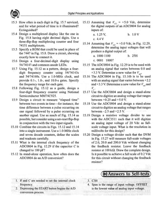
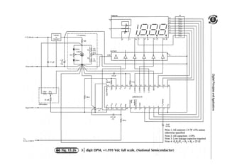
3i digit DVM, Four decade; ±0.2, +0.2, ±20, and ±200 Vdc (National Semiconductor)
33. Technical specifications
DC volts < ± I% accuracy
ranges 2 V, 20 V, 200 V, 2 kV
input impedance 2 V range, > IO Mn
20 V to 2 kV range, 10 MQ
AC RMS volts < ± l% accuracy
ranges 2 V, 20 V, 200 V, 2 kV
(40 to 5 kHz sinewave)
DC amps < ± I% accuracy
ranges 200 µA, 2 mA, 20 mA, 200mA, 2A
Ohms < ± l% accuracy
ranges 200 n, 2Hl. 20kQ, 200kQ, 2 MQ
'Al MU
tll«i
1 ~' ---¥Iv--,
,v
20 -
~
'1MU
OJ""
i'""
J:!U
~ V
}fl'
',,l!s
Note I: All V,, connections should use a single Vee
point and all ground/analog ground connection should
use a single ground/analog ground point.
Note 2: All resistors are 1/4 watt unless otherwise
specified
Note 3: All capacitors arc ±10%
Note 4: All op amps have a 0. I /IF capacitor
connected across the V+ and V- supplier
Note 5: All diodes arc IN914
l2lH2
:,.;s115w,
J.10tl
"··'~ L. 111 ·I II l1
1
t
la,
~1
<JV.=.,.
:J; il ' !~,,
l'I J.. ~l.l.1h( ,~?
IOHl~ ~U
1)0~0
~
,.,..
"°'.""~ """" ' ~ L--+-~____.__....-t-1-4--~
01~. JrnlV ,,_.!-:-°
l j ( ~
JOµl nn
d~:,
.....
X2(l
!Oll~O
nc o !':,
Ohnis
Cr,nmwn WHl!"-•
Vuhs
amp·,°--
Ohu1{
I LU l~ l
~ l p A
... '""'•
!OHU!"·020m,
1~ ~z.1•~]00 mA9 r
~ 1 ,
I ~l l"i,
rcc-1'-
;
...
l){'I .~,,- ~ ~ c ; - W v - ~
lK AC
M<,U 1~,,
J'lf>U!I·!, ·1
~ l ) f . ) U
2U!
l'lf,Hl 1"~
~
;;::. PJ.d
h'-'
11HJ I H"'
,r
511!
,~ ~t=1'II./). Ht
H)9 r
~ ~ 1 U
1.w,:-.mo !~o
""'"' l~;:·
~'"·::'""J.~t.LLLLL.1~ 11'
*•U71if
N :;..
l5Wt.J
1>D-1~Hl /•1" ,,ht dit!it;i! m"1mnd,·r
::;::1011F
tru
tU7
,,,
I ' o,:::'fifl"''"' " /1 15 f,l PP
A low-cost DMM using the ADD 3501 (National Semiconductor Data Acquisition Handbook)
~~H:
t:::)
<cl'
:::;:
~
-0
5·
C')
-s·
cn
"'
~
Q.
~
£
g.
::i
"'
34. Applications
The different de and ac voltage ranges are accommodated by a resistive voltage divider at the analog input.
Alternating-current voltages are measured by using the three operational amplifiers A3
,A;" and A5
to develop
a de voltage that is proportional to the root-mean-square (RMS) value ofthe ac input voltage.
Measurement Range Frequency
Accuracy
Overrange
mode 0.2 2.0 20 200 2000 response display
DC volts - V V V V - :S: 1%FS ±OFLO
AC volts VRMS VRMS VRMS VRMS 40 Hzto 5 kHz :S: 1%FS +OFLO
DC amps mA mA mA mA mA - :S: 1%FS ±OFLO
ACamos mARMS mARMS mARMS mARMS mARMS 40 Hz to 5 kHz :S: 1%FS +OFLO
Ohms kQ kQ kQ kQ kQ - :S: 1% FS +OFLO
Performance of the DMM in Fig. 15.28
A series ofcurrent-sensing resistors are used to measure either de or ac current. The current to be measured
is passed through one of the sensing resistors, and the DMM digitizes the voltage developed across the
resistor.
The DMM measures resistance by applying a known current from an internal current source (operational
amplifiers A1
and A) to the unknown resistance and then digitizing the resulting voltage developed.
For those interested in pursuing this subject, complete details for the construction and calibration of this
DMM are given in the National Semiconductor Data Acquisition Handbook.
The pri~ary objectiveof fhischapter is todemonstrate the useof ~any ofthe most fundamental prindples
discussed throughout the text by considering some of the more common digital circuit configurations
encountered in industry. Multiplexing of LED displays, time and frequency measurement, and use of
digital voltmeters ofall types are widely used throughout industry.Although our coverage is byno means
comprehensive, it will~rve as an excellent introduction to industrial pr<!ctices,
The problems at the t'!lld of this chapter will also provide ag®d transition into industry. They are in
general longer than previou$1y assigned problems. All the necessary informationrequired to worka given
problem may not be given:-this isintentional.since it will require y()u.to seekinformation from industrial
data sheets. However, the problems aremore,0£a designnature, and usually deal with a practical,functional
circuit that can be 11sedfo accomplish a given task; as such, they are much more interesting and satisfying
to solve.
In order to solve some ofthese problems, you may
have to consult product data sheets that are not in-
cluded in this text. It is intended that you discover a
source for such information.
15.1 Pick one ofthe solutions suggested in Example
15.3 and do a detailed design, including part
numbers and pin numbers.
15.2 Design a four-decimal-digit multiplexed dis-
play like the one in Fig. 15.7, but use com-
mon-cathode-type LEDs. Use a basic circuit
like the one in Fig. 15.2, bu.t you will now
·need to generate DIGIT waveforms that have
positive pulses.
35. Digital Principles andApplications
15.3 How often is each digit in Fig. 15.7 serviced,
and for what period of time is it illuminated?
Extinguished?
15.4 Design a multiplexed display like the one in
Fig. 15.8 having eight decimal digits. Use a
three-flip-flop multiplexing counter and four
74151 multiplexers.
15.5 Specify a ROM that could be used in place of
the 7447 in Fig. 15.8. Draw a circuit, showing
exactly how to connect it.
15.6 Design a four-decimal-digit display using
54/74141 and common-anode LEDs.
15.7 Using Fig. 15.12 as a pattern, design a four-
digit frequency counter using 54174143s
and 54174160s. Use a 1.0-MHz clock, and
provide 0.1-, 1.0-, and 10.0-s gates. Specify
the frequency range for each gate.
15.8 Following Fig. 15.12 as a guide, design a
four-digit frequency counter using National
Semiconductor MM74C925.
15.9 Design a circuit to measure "elapsed time"
between two events in time-for instance, the
time difference betveen a pulse occurring on
one signal followed by a pulse occurring on
another signal. Use as much of Fig. 15.14 as
possible, butconsider using a set-resetflip-flop
in conjunction with the two input signals.
15.10 Combine the circuits in Figs. 15.12 and 15.14
into a single instrument. Use a 1.0-MHz clock
.and seven decade counters, define the scales
and readouts carefully.
15.11 What is the internal clock frequency of the
ADC0804 in Fig. 12.29 if the capacitor C is
changed to 100 pF?
15.12 In stand-alone operation, how often does the
ADC0804 do an AID conversion?
1. R and C are needed to the internal clock
frequency.
2. Depressing the STARTbuttonbegins the AID
conversion process.
15.13 Assuming that Vee = +5.0 Vdc, determine
the digital outputs of an ADC0804 for analog
inputs of:
a. 1.25 V, b. 1.0 V
C. 4.4 V
15.14 Assuming that Vee= +5.0 Vdc, in Fig. 12.29,
determine the analog input voltages that will
produce a digital output of:
a. 1000 1100 b. 25H
C. 0001 1000?
15.15 The ADC0804 in Fig. 12.29 is to be used with
an analog signal that varies between 0.0 and
+3.3 V. Determine a new value for V,er
15.16 The ADC0804 in Fig. 15.16b is to be used
with an analog signal that varies between +2.2
and+3.3 V. Determine a new value for V,erand
V.
,-
15.17 Use the ADC0804 and design a stand-alone
circuit to digitize an analog voltage that ranges
between +0.25 and +5.0 V.
15.18 Use the ADC0804 and design a stand-alone
circuit to digitize an analog voltage that ranges
between -2.5 and +2.5 V.
15.19 Design a resistive voltage divider to use
with the ADC3511 such that it will digitize
an analog input voltage of 20 Vde as full-
scale voltage input. What is the resolution in
millivolts for this design?
15.20 Design a voltage divider such that the DVM
in Fig. 15.27 will measure full-scale voltages
of2.0, 20.0 and 200.0 Vdc without changing
the feedback resistor. Leave the feedback
resistor at 100 kQ. Draw the complete design.
Is it possible to achieve a full scale of0.2 Vdc
for this circuit without changing the feedback
resistor?
3. C3H
4. Span is the range ofinputvQltage, OFFSET,
is the lowest value ofanalog input voltage.