SlideShare a Scribd company logo
1 of 18
Download to read offline
controlled by the control signals generated by timing and
control unit.
2.7. COMPARISON OF MICROPROCESSOR AND
MICROCONTROLLER
Microcontroller
S.No Microprocessor
1. It is a general purpose It is a special purpose
1
digital computer. digital computer.
It contains CPU, It contains CPU, Timers/
memory| Counters, serial and
addressing circuits,parallel 1/0 ports,
handlingInternal RAM, Internal
ROM etc.,
2.
registers,
interrupt
circuits etc.,
2.08
3. It has many op-codes | It has one or two
op-codes for moving
3.
for moving data from
extenal memory to the data from external|
CPU. memory to the CPU.
It has one or two bit
handling instructions.
It has many bit handling
instructions.
To function as computer,
4.
To function as computer,
5
it needs additional it does not need any
external parts. external parts.
6 Examples: 8085,8086, Exampes: 8051,8048,
Z80 etc. 8052 etc.,
2.8.SIGNAL DESCRIPTION OF 8051
PLO
40cc
PI.I2 39 PO.0/ADO
P1.2 3 38PO.1/ADI
37P0.2/AD2
36P0.3/AD3
P13 4
P14 5
PI.5 6
P16 7
35PO4/AD4
34 P0.5/AD5
P1.7 8
RESET9
(RXD)P3.010 IC 8051 31 EAVPP
33PO.6/AD6
32PO.7/AD7
TXD)P3.1 30AL.E/PROG
INTO)P3.2 12
INTT)P3.3 13
29 PSEN
28 P2.7/A15
(TOP34 14
(TI)P3.5 15
(WRP3.6 16
27P2.6/A14
26P2.5/A13
25 P2.4/A12
(RD)P3.7 7
XTAL2 18
XTALI 19
s 20
24P2.3/A11
23P2.2/A10
22P2.1/A9
21P2.0/A8
Fig. 2.2 Pindiagram of 8051
2.09
M i c r o c o n t r o l l e r
8051
is
a v a i l a b l e
in a 40 pin plastin
ceramic
DIP
p a c k a g e s .
The pin
diagram
of8051 is shou
a 40 pin plastic and
1 is show in
the fig.2.2.
b ) V s s :
It is a
return pin for the supply
(Ground).
b)
) V o c :
It is a +5Vsupply
voltage
pin.
a)
to reset the
c) m i c r o c o n t r o l l e r .
RESET:
The
reset pin is used to reset the
e
d
indicates that the valid address bits are available
their respective pins. This ALE signal is valid only for
external memory
accesses. This pin also act as
program pulse input during on-chip EPROM
programming.
d)ALE/PROG:Theaddress latch enable output pulse
on
e) EAVpp: External access pin, iftied low, indicates
that the 8051 can address external program memory.
For execution of programs in internal program
memory this pin must be tied high. This pin also
receives 21 Voits for programming the on-chip
EPROM.
PSEN: This program store enable pin is not activated
for internal fetches. It is activated when the CPU IS
accessing external program memory. PSEN I
activated twice every cycle.
g) Port0 (PO.0 P0.7): Port 0 acts as an 8"
bidirectional bit/byte addressable /O port. This ra
as
been allotted an
address in the SFR address rany
range
(ADa-AD) during external memory access.
also receives code bytes during
programming
Port 0 acts as
multiplexed address and data i
R address
ess and data line:
0
internal EPROM. the
h) Port 1(P1.0 -
P1.7): Port 1 acts as an 8-bit
h)
bidirectional bit/byte addressable port. It has been
allotted an address in the SFR address range.
i)Port 2 (P2.0 P2.7): Port2 acts as 8-bit bidirectional
bitbyte addressable l/O port. It has been allotted an
address in the SFR address range.
During external memory access, port 2 emits
higher eight bits of address (As - A15). Port 2 also
receives higher order address bits during
programming on the on-chip EPROM.
Port 3 (P3.0- P3.7): Port 3 is an 8-bit bidirectional bit/
byte addressable l/0 port. It has been allotted an
address in the SFR address range. The port 3 pins
also serve the alternate functions as listed in the table
below.
Port Pins Alternate Functions
P3.0 RXD (Serialinputport)
P3.1 TXD (Serial output port)
P3.2 INTO (External interrupt 0)
P3.3 INT1. (External interrupt 1)
P3.4 TO (Timer/Counter0 external input)
P3.5 T1 (Timer/Counter 1 external input)
P3.6 WR (External data memory write strobe)
P3.7 RD (External data memory read strobe)
2.11
XTALI and XTAL2
There is an in-built oscillato.
which derives the necessary clock frequency for tha
operation of the oscillator. XTAL1 is the input to the
inverting oscillator amplifier. XTAL2 is the output from
the inverting oscillator amplifier.
ALLL
(ARITHMETIOAND LOCIR IAITV
Spaces.
2.11.1. ROM (Program memory)
Program memory can only be read, not written to.
There can be upto 64 Kbytes of program memory. In the
ROM and EPROM versions, the lowest 4 Kbytes are
provided on-chip. In the ROM less versions all program
memory is external (off-chip). The 64 Kbyte program memoiy
2.14
space consists of an internal and external memory portions.
The memory map structure of program memory is shown in
the fig. 2.3.
In microcontroller 8051, the lower 4 Kbytes of program
memory can be placed either in the on-chip ROM or in an
external ROM. This selection is made by strapping the EA
pin to either Vcc or Vss. If the EA pin is held high, the
program fetches to addresses 0000H through OFFFH are
directed to the internal ROM. Program fetches to addresses
1000H through FFFFH are directed to the external ROM.
FFFF
EXTERNAAL
EA -0 or1
1000L
OFFF OFFF
EXTERNAL
(EA=0)
INTERNAL
CEA = 1)
Fig. 2.3 Memory map of program memory
If the EA pin is held low, the microcontroller 8051
etches all instructions from external program memory. The
read strobe to external ROM, PSEN is used for all program
fetches. PSEN is not activated for internal program fetches.
Locations 00 through 23H in program memory are
used by interrupt service routine.
2.15
The data
memory
address
space
consists ns
memory
The
2.11.2.
RAM (Data
memory)
of an
internal and
external
memory
spaces.
External datamer
is accessed,
when a
MOVX
i n s t r u c t i o n
is executed
structure of data memory
is
shown in the fig.2.4.
FFFFU
INTERNAL DATA
MEMORY
EXTERNAL
DATA
MEMORY
FFH SPECIAL
(64 Kby tes)
FUNCTION
RECISTER
128 bytes
sOH
7FH
INTERNAL
DATA RAM
128 bytes
00L1 0000H
Fig.2.4 Memory, map ofdata memory
Internal data memory is divided into two physically
separate and distinct blocks. They are,
i) The lower 128 bytes of RAM (internal RAM) area, and
i) The upper 128 bytes of special function register (RAM)
area
The address range of internal RAM is from 00H to
7FH, and the address range of SFR is from 80H and FFH.
The structure of internal data memory space is sno n
in the fig.2.5. Four 8-bit register banks occupy locations
through 31 in lower RAM area. Only one of these banks may
2.16
he enabled at a time, through a two bit field in PSW. The next
16-bytes, locations 32 through 47 contain 128 bit
addressable locations. Again the next 80 bytes, locations 48
through 127 contain only byte addressable locations. The SFR
area also has byte and bit addressable locations. Internal
data memory addresses are always one byte wide. All the
bytes in the lower 128 can be accessed by either direct or
indirect addressing. The SFRs are accessed by only direct
addressing.
255 FOH
EOH
DOH-
B8H
Special
function
BOH
ADDRESABLE
BITS IN SFRs
registers
A8H
AOH
98H
90H
88H
128 80H
127
48
128 120
ADDRESABLE
BITS IN RAM
32 7 (128 BITS)
R BANK 3
24 R
R1
INTERNAL BANK 2
DATA RAM 16 REGISTERS
R BANK1
8 R
R
BANK
R
Fig. 2.5 Structure of internal data memory space
2.17
The CPU generates RD and WR signals as needed
during external RAM accesses. There can be up to 64 Kbytes
of external data memory. Memory addresses can be either 1
or 2 bytes wide. Only indirect addressing can be used for
accessing external data memory. In one byte addresses, the
location is indirectly specified either in register R0 or R1, which
is specified as @Ri. In two byte addresses, the location is
indirectly specified in register DPTR, specified as @DPTR. In
all external data RAM accesses, the accumulator is always
the destination or source of the data. The external RAM IS
activated only during the execution of a MOVX instruction.
2.11.3. Internal RAM memory map
7F
Only byte
3.05
34. ADDRESSING MODES
The ways by which the addresses are specified in the
struction are called addressing modes. Generally, the data
sters or emory. But we can call for accessing the data
in different modes. Hence the ways of accessingdata are
required
reQuired for manipulating instructions are either placed in
called addressing modes.
The microcontroller 8051 provides five addressing
modes. Theyare
a) Immediate addressing
b) Direct addressing
Indirect addressing
d) Register addressing
e) Index addressing
a) Immediate addressing mode
In this mode of addressing, an immediate data i.e. a
constant is specified in the operand field. By using this
addressing mode, we can move
immediate data and also
doing arithmetic and logical operations
with immediate data.
All immediate data are proceded by a hash (#) symbol.
Example
MOV A, #64H
This
instruction
loads the
A c c u m u l a t o r
with the
hexadecimal data of 64H.
b) Register addressing
mode
In this mode of
addressing,
operands
are
stored in
registers from RO to R7 of the
s e l e c t e d
register
bank:
the
3.06
When the instruction is executed, one of the eight
registersin
the selocted register bank is accessed. One of the
four banks
selec
bits in the PSW register. The least significant three bito
to be used,
is selected at the execution time by using the two ba
bits of the
instruction op-code indicate which register is to be
Acc B, DPTR and CY (boolean process
accumulator) can also be addressed as registers.
Example:
MOV A, R3
This instruction moves the data from register R3 into
Accumulator.
c) Direct addressing Mode
In this mode of
addressing, the operand is specified
by an 8-bit address field in the instruction format. Only
internal data
RAM(lower 128 bytes) and special function
registers can be
directly addressed.
Example:
MOV direct, A
This
instruction moves the content of
accumulator
of accumulator to
direct address directly.
NOTE: Direct is the
address of either lower 128 byi
lower 128 byte
internal data
memory or
special function regis
inction register.
d) Indirect addressing mode
In this mode of
addressing, the
instructi a
ction specifie
register which contains the
address of the
operand. Both
internal and external RAM can be
addressed indirectily.
3.07
address register for 8-6it address can be RO or
oftheselec
of thister for 16-bit address can only be the 16-bit
ected register bank, or the stack pointer. The
d a t ap o i n t e r ( D P T R ) .
oE& bytes of external data memory can be specified
The address of 128 bytes of internal RAM and the
dóress
space is accomplished using the 16-bit DPTR. The
ress register for
lower2 5 6
in register Ro 1. The full 64 Kbytes data memory
cial function registers are not to be accessed by this
method.
Execution of PUSH and POP instructions also uses
register-indirect addressing.
Example:
a)MOVR1, A
This instruction moves the coutent of Acc to the
internal RAM location, specified by the register R1.
b) MOVX A, @DPTR
This instruction moves the content of external RAM
memory location specified by DPTR to Acc.
e) Index addressing mode
Index addressing mode is otherwise called as base
egister plus index register indirect addressing
intended for reading look-up table in program memory.
COunter) points to the base of the table and the Accumulator
Arde..ny program memory can be accessed with index
addressing,
ining, and it can only be read. This addressing mode is
A 16-bit base register (either DPTR or the program
3.08
ress of the
table
is setup with the table entry number. The address of th
entry in program memory is formed by adding the conte
of Accumulator and the base register.
In the case of jump instructions, the
content
Accumulator is added with one ot the
specified 18
of
6-bit
registers to form the jump destination address.
Example:
a) MOVCA, @A+DPTR
The content of program memory, which address is
specified by the sum of the contents of the registers
A and DPTR is moved into Accumulator.
b)JMP@A+DPTR
The control of microcontroller is transferred to the
memory location, which is the sum of the addresses
specified by Accumulator and DPTR. Actually the sum
of the contents of Accumulator and DPTR is loaded
into the program counter.
3.5. DATA
TRANSFER INSTRUCTIONs
Data transfer instructions are divided into three
classes. They are,
a) General purpose instructions
b) Accumulator specific instructions, and
c) Address- object instructions.
a) General purpose data transfer instructions
There are 3
major types of instructions u
used for
transferring data in
general purpose.
IS moved Trom one place to anotner place. Except a
iS moved Trom one place to another place. cept a
POP PSW or MOV directly to the PSW instruction, the
conditional flag settings are not affected. do ho>
he byte level data transfer instructions are described belownStruc
1) MOV A, Rn (Move register to Accumulator)
S
(A) (Rn)
The content of the register Rn is copied into the
Accumulator
2) MOV A, direct.(Move direct byte to Accumulator)
(A) (direct)
3.10
The content of directly addressed location
is copied
into the Accumulator.
3) MOV A. @Ri (Move indirect RAM to Accumulatol
((Ri)
ator)
(A)
The content of memory location, which is
ddressed
by the register Ri is copied in to the Accumulato.
Accumulato
4) MOV A, #data (Move immediate data to the Accumula
(A) #data
The content of second byte of the instruction is
copied into the Accumulator
5) MOV Rn. A (Move Accumulator to register)
(Rn) (A)
The content of accumulator is copied into the register Rn.
6) MOV Rn, direct (Move direct byte to Register)
(Rn) (direct)
The content of directly addressed location is copie0
into register Rn.
7) MOV Rn, #data (Move immediate data to register)
(Rn) #data
is
The content of the second byte of the instrucio
copied into the register Rn.
8) MOV direct, A (Move Accumulator to direct byte)
(direct) (A)
The content of Accumulator is copied into the
directly
specified location.
3.11
MOVdirect, Rn (Move register to direct byte)
(direct) (Rn)
The content of register Rn is copied into the directly
specified location.
MOV direct, direct (Move direct byte to direct byte)
(direct) (direct)
The content of location directly specified in the source
ocerand is copied into another directly specified location ir
ne destination operand.
11) MOV direct, @Ri
(direct) (R)
The content of memory location, which is addressed
by the register Ri is copied in to the directly specified
location.
12) MOV direct, #data
(direct) #data
The content of third byte of the instruction is copied in
to the directly specified location.
13) MOV @Ri, A (Move Accumulator to indirect RAM)
((Ri)) (A)
The content of Accumulator is copied into the internal
AM
memory location, which address is specified in the
egister Ri.
4) MOV @Ri, direct (Move direct byte to indirect RAM)
((Ri)) (direct)
3.12
The content of directly specified location is copied into
internal RAM location, which address is specified in the
register Ri (RO or R1)
15) MOV @Ri, #data (Move immediate data to indirect RAM)
((Ri)) #data
The content of second byte of the instruction is
The
copied into internal RAM location, which address is specified
in the register Ri (RO or R1)

More Related Content

Similar to assignment 1-MC.pdf

Architecture of 8051 microcontroller))
Architecture of 8051 microcontroller))Architecture of 8051 microcontroller))
Architecture of 8051 microcontroller))Ganesh Ram
 
Pc based wire less data aquisition system using rf(1)
Pc based wire less data aquisition system using rf(1)Pc based wire less data aquisition system using rf(1)
Pc based wire less data aquisition system using rf(1)Vishalya Dulam
 
SYBSC IT SEM IV EMBEDDED SYSTEMS UNIT III The 8051 Microcontrollers
SYBSC IT SEM IV EMBEDDED SYSTEMS UNIT III  The 8051 MicrocontrollersSYBSC IT SEM IV EMBEDDED SYSTEMS UNIT III  The 8051 Microcontrollers
SYBSC IT SEM IV EMBEDDED SYSTEMS UNIT III The 8051 MicrocontrollersArti Parab Academics
 
Assembly programming
Assembly programmingAssembly programming
Assembly programmingOmar Sanchez
 
8051 microcontroller
8051 microcontroller 8051 microcontroller
8051 microcontroller nitugatkal
 
8051 architecture
8051 architecture8051 architecture
8051 architecturesb108ec
 
Architecture of the Intel 8051 Microcontroller
Architecture of the Intel 8051 MicrocontrollerArchitecture of the Intel 8051 Microcontroller
Architecture of the Intel 8051 MicrocontrollerSudhanshu Janwadkar
 
Fundamentals of Microcontroller 8051 by Dr. Jogade S M, Assistant Professor, ...
Fundamentals of Microcontroller 8051 by Dr. Jogade S M, Assistant Professor, ...Fundamentals of Microcontroller 8051 by Dr. Jogade S M, Assistant Professor, ...
Fundamentals of Microcontroller 8051 by Dr. Jogade S M, Assistant Professor, ...sangeeta jogade
 
janakiraman egsp collage I msc 4 unit
janakiraman egsp collage  I msc 4 unitjanakiraman egsp collage  I msc 4 unit
janakiraman egsp collage I msc 4 unitjanakiramang6
 
8096 microcontrollers notes
8096 microcontrollers notes8096 microcontrollers notes
8096 microcontrollers notesDr.YNM
 
Study of 8051 microcontroller
Study of 8051 microcontrollerStudy of 8051 microcontroller
Study of 8051 microcontroller918007165995
 

Similar to assignment 1-MC.pdf (20)

Micro 8051
Micro 8051Micro 8051
Micro 8051
 
Architecture of 8051 microcontroller))
Architecture of 8051 microcontroller))Architecture of 8051 microcontroller))
Architecture of 8051 microcontroller))
 
Pc based wire less data aquisition system using rf(1)
Pc based wire less data aquisition system using rf(1)Pc based wire less data aquisition system using rf(1)
Pc based wire less data aquisition system using rf(1)
 
SYBSC IT SEM IV EMBEDDED SYSTEMS UNIT III The 8051 Microcontrollers
SYBSC IT SEM IV EMBEDDED SYSTEMS UNIT III  The 8051 MicrocontrollersSYBSC IT SEM IV EMBEDDED SYSTEMS UNIT III  The 8051 Microcontrollers
SYBSC IT SEM IV EMBEDDED SYSTEMS UNIT III The 8051 Microcontrollers
 
Assembly programming
Assembly programmingAssembly programming
Assembly programming
 
8051 microcontroller
8051 microcontroller 8051 microcontroller
8051 microcontroller
 
Micro controller
Micro controllerMicro controller
Micro controller
 
Microcontroller1
Microcontroller1Microcontroller1
Microcontroller1
 
8051 architecture
8051 architecture8051 architecture
8051 architecture
 
unit-2.pptx
unit-2.pptxunit-2.pptx
unit-2.pptx
 
Pic full note
Pic full notePic full note
Pic full note
 
8051 microcontroller
8051 microcontroller8051 microcontroller
8051 microcontroller
 
Architecture of 8085
Architecture of 8085Architecture of 8085
Architecture of 8085
 
Architecture of 8085
Architecture of 8085Architecture of 8085
Architecture of 8085
 
002079
002079002079
002079
 
Architecture of the Intel 8051 Microcontroller
Architecture of the Intel 8051 MicrocontrollerArchitecture of the Intel 8051 Microcontroller
Architecture of the Intel 8051 Microcontroller
 
Fundamentals of Microcontroller 8051 by Dr. Jogade S M, Assistant Professor, ...
Fundamentals of Microcontroller 8051 by Dr. Jogade S M, Assistant Professor, ...Fundamentals of Microcontroller 8051 by Dr. Jogade S M, Assistant Professor, ...
Fundamentals of Microcontroller 8051 by Dr. Jogade S M, Assistant Professor, ...
 
janakiraman egsp collage I msc 4 unit
janakiraman egsp collage  I msc 4 unitjanakiraman egsp collage  I msc 4 unit
janakiraman egsp collage I msc 4 unit
 
8096 microcontrollers notes
8096 microcontrollers notes8096 microcontrollers notes
8096 microcontrollers notes
 
Study of 8051 microcontroller
Study of 8051 microcontrollerStudy of 8051 microcontroller
Study of 8051 microcontroller
 

Recently uploaded

如何办理萨省大学毕业证(UofS毕业证)成绩单留信学历认证原版一比一
如何办理萨省大学毕业证(UofS毕业证)成绩单留信学历认证原版一比一如何办理萨省大学毕业证(UofS毕业证)成绩单留信学历认证原版一比一
如何办理萨省大学毕业证(UofS毕业证)成绩单留信学历认证原版一比一ga6c6bdl
 
Vip Udupi Call Girls 7001305949 WhatsApp Number 24x7 Best Services
Vip Udupi Call Girls 7001305949 WhatsApp Number 24x7 Best ServicesVip Udupi Call Girls 7001305949 WhatsApp Number 24x7 Best Services
Vip Udupi Call Girls 7001305949 WhatsApp Number 24x7 Best Servicesnajka9823
 
Slim Call Girls Service Badshah Nagar * 9548273370 Naughty Call Girls Service...
Slim Call Girls Service Badshah Nagar * 9548273370 Naughty Call Girls Service...Slim Call Girls Service Badshah Nagar * 9548273370 Naughty Call Girls Service...
Slim Call Girls Service Badshah Nagar * 9548273370 Naughty Call Girls Service...nagunakhan
 
Call Girls In Paharganj 24/7✡️9711147426✡️ Escorts Service
Call Girls In Paharganj 24/7✡️9711147426✡️ Escorts ServiceCall Girls In Paharganj 24/7✡️9711147426✡️ Escorts Service
Call Girls In Paharganj 24/7✡️9711147426✡️ Escorts Servicejennyeacort
 
Gaya Call Girls #9907093804 Contact Number Escorts Service Gaya
Gaya Call Girls #9907093804 Contact Number Escorts Service GayaGaya Call Girls #9907093804 Contact Number Escorts Service Gaya
Gaya Call Girls #9907093804 Contact Number Escorts Service Gayasrsj9000
 
(办理学位证)加州州立大学北岭分校毕业证成绩单原版一比一
(办理学位证)加州州立大学北岭分校毕业证成绩单原版一比一(办理学位证)加州州立大学北岭分校毕业证成绩单原版一比一
(办理学位证)加州州立大学北岭分校毕业证成绩单原版一比一Fi sss
 
(办理学位证)多伦多大学毕业证成绩单原版一比一
(办理学位证)多伦多大学毕业证成绩单原版一比一(办理学位证)多伦多大学毕业证成绩单原版一比一
(办理学位证)多伦多大学毕业证成绩单原版一比一C SSS
 
Hifi Babe North Delhi Call Girl Service Fun Tonight
Hifi Babe North Delhi Call Girl Service Fun TonightHifi Babe North Delhi Call Girl Service Fun Tonight
Hifi Babe North Delhi Call Girl Service Fun TonightKomal Khan
 
1:1原版定制美国加州州立大学东湾分校毕业证成绩单pdf电子版制作修改#真实留信入库#永久存档#真实可查#diploma#degree
1:1原版定制美国加州州立大学东湾分校毕业证成绩单pdf电子版制作修改#真实留信入库#永久存档#真实可查#diploma#degree1:1原版定制美国加州州立大学东湾分校毕业证成绩单pdf电子版制作修改#真实留信入库#永久存档#真实可查#diploma#degree
1:1原版定制美国加州州立大学东湾分校毕业证成绩单pdf电子版制作修改#真实留信入库#永久存档#真实可查#diploma#degreeyuu sss
 
办理(CSU毕业证书)澳洲查理斯特大学毕业证成绩单原版一比一
办理(CSU毕业证书)澳洲查理斯特大学毕业证成绩单原版一比一办理(CSU毕业证书)澳洲查理斯特大学毕业证成绩单原版一比一
办理(CSU毕业证书)澳洲查理斯特大学毕业证成绩单原版一比一diploma 1
 
专业一比一美国旧金山艺术学院毕业证成绩单pdf电子版制作修改#真实工艺展示#真实防伪#diploma#degree
专业一比一美国旧金山艺术学院毕业证成绩单pdf电子版制作修改#真实工艺展示#真实防伪#diploma#degree专业一比一美国旧金山艺术学院毕业证成绩单pdf电子版制作修改#真实工艺展示#真实防伪#diploma#degree
专业一比一美国旧金山艺术学院毕业证成绩单pdf电子版制作修改#真实工艺展示#真实防伪#diploma#degreeyuu sss
 
(办理学位证)韩国汉阳大学毕业证成绩单原版一比一
(办理学位证)韩国汉阳大学毕业证成绩单原版一比一(办理学位证)韩国汉阳大学毕业证成绩单原版一比一
(办理学位证)韩国汉阳大学毕业证成绩单原版一比一C SSS
 
定制(USF学位证)旧金山大学毕业证成绩单原版一比一
定制(USF学位证)旧金山大学毕业证成绩单原版一比一定制(USF学位证)旧金山大学毕业证成绩单原版一比一
定制(USF学位证)旧金山大学毕业证成绩单原版一比一ss ss
 
Call Girls Service Kolkata Aishwarya 🤌 8250192130 🚀 Vip Call Girls Kolkata
Call Girls Service Kolkata Aishwarya 🤌  8250192130 🚀 Vip Call Girls KolkataCall Girls Service Kolkata Aishwarya 🤌  8250192130 🚀 Vip Call Girls Kolkata
Call Girls Service Kolkata Aishwarya 🤌 8250192130 🚀 Vip Call Girls Kolkataanamikaraghav4
 
NO1 Qualified Best Black Magic Specialist Near Me Spiritual Healer Powerful L...
NO1 Qualified Best Black Magic Specialist Near Me Spiritual Healer Powerful L...NO1 Qualified Best Black Magic Specialist Near Me Spiritual Healer Powerful L...
NO1 Qualified Best Black Magic Specialist Near Me Spiritual Healer Powerful L...Amil baba
 
5S - House keeping (Seiri, Seiton, Seiso, Seiketsu, Shitsuke)
5S - House keeping (Seiri, Seiton, Seiso, Seiketsu, Shitsuke)5S - House keeping (Seiri, Seiton, Seiso, Seiketsu, Shitsuke)
5S - House keeping (Seiri, Seiton, Seiso, Seiketsu, Shitsuke)861c7ca49a02
 
vip Model Basti Call Girls 9999965857 Call or WhatsApp Now Book
vip Model Basti Call Girls 9999965857 Call or WhatsApp Now Bookvip Model Basti Call Girls 9999965857 Call or WhatsApp Now Book
vip Model Basti Call Girls 9999965857 Call or WhatsApp Now Bookmanojkuma9823
 
Hifi Defence Colony Call Girls Service WhatsApp -> 9999965857 Available 24x7 ...
Hifi Defence Colony Call Girls Service WhatsApp -> 9999965857 Available 24x7 ...Hifi Defence Colony Call Girls Service WhatsApp -> 9999965857 Available 24x7 ...
Hifi Defence Colony Call Girls Service WhatsApp -> 9999965857 Available 24x7 ...srsj9000
 

Recently uploaded (20)

如何办理萨省大学毕业证(UofS毕业证)成绩单留信学历认证原版一比一
如何办理萨省大学毕业证(UofS毕业证)成绩单留信学历认证原版一比一如何办理萨省大学毕业证(UofS毕业证)成绩单留信学历认证原版一比一
如何办理萨省大学毕业证(UofS毕业证)成绩单留信学历认证原版一比一
 
Vip Udupi Call Girls 7001305949 WhatsApp Number 24x7 Best Services
Vip Udupi Call Girls 7001305949 WhatsApp Number 24x7 Best ServicesVip Udupi Call Girls 7001305949 WhatsApp Number 24x7 Best Services
Vip Udupi Call Girls 7001305949 WhatsApp Number 24x7 Best Services
 
young call girls in Khanpur,🔝 9953056974 🔝 escort Service
young call girls in  Khanpur,🔝 9953056974 🔝 escort Serviceyoung call girls in  Khanpur,🔝 9953056974 🔝 escort Service
young call girls in Khanpur,🔝 9953056974 🔝 escort Service
 
Slim Call Girls Service Badshah Nagar * 9548273370 Naughty Call Girls Service...
Slim Call Girls Service Badshah Nagar * 9548273370 Naughty Call Girls Service...Slim Call Girls Service Badshah Nagar * 9548273370 Naughty Call Girls Service...
Slim Call Girls Service Badshah Nagar * 9548273370 Naughty Call Girls Service...
 
young call girls in Gtb Nagar,🔝 9953056974 🔝 escort Service
young call girls in Gtb Nagar,🔝 9953056974 🔝 escort Serviceyoung call girls in Gtb Nagar,🔝 9953056974 🔝 escort Service
young call girls in Gtb Nagar,🔝 9953056974 🔝 escort Service
 
Call Girls In Paharganj 24/7✡️9711147426✡️ Escorts Service
Call Girls In Paharganj 24/7✡️9711147426✡️ Escorts ServiceCall Girls In Paharganj 24/7✡️9711147426✡️ Escorts Service
Call Girls In Paharganj 24/7✡️9711147426✡️ Escorts Service
 
Gaya Call Girls #9907093804 Contact Number Escorts Service Gaya
Gaya Call Girls #9907093804 Contact Number Escorts Service GayaGaya Call Girls #9907093804 Contact Number Escorts Service Gaya
Gaya Call Girls #9907093804 Contact Number Escorts Service Gaya
 
(办理学位证)加州州立大学北岭分校毕业证成绩单原版一比一
(办理学位证)加州州立大学北岭分校毕业证成绩单原版一比一(办理学位证)加州州立大学北岭分校毕业证成绩单原版一比一
(办理学位证)加州州立大学北岭分校毕业证成绩单原版一比一
 
(办理学位证)多伦多大学毕业证成绩单原版一比一
(办理学位证)多伦多大学毕业证成绩单原版一比一(办理学位证)多伦多大学毕业证成绩单原版一比一
(办理学位证)多伦多大学毕业证成绩单原版一比一
 
Hifi Babe North Delhi Call Girl Service Fun Tonight
Hifi Babe North Delhi Call Girl Service Fun TonightHifi Babe North Delhi Call Girl Service Fun Tonight
Hifi Babe North Delhi Call Girl Service Fun Tonight
 
1:1原版定制美国加州州立大学东湾分校毕业证成绩单pdf电子版制作修改#真实留信入库#永久存档#真实可查#diploma#degree
1:1原版定制美国加州州立大学东湾分校毕业证成绩单pdf电子版制作修改#真实留信入库#永久存档#真实可查#diploma#degree1:1原版定制美国加州州立大学东湾分校毕业证成绩单pdf电子版制作修改#真实留信入库#永久存档#真实可查#diploma#degree
1:1原版定制美国加州州立大学东湾分校毕业证成绩单pdf电子版制作修改#真实留信入库#永久存档#真实可查#diploma#degree
 
办理(CSU毕业证书)澳洲查理斯特大学毕业证成绩单原版一比一
办理(CSU毕业证书)澳洲查理斯特大学毕业证成绩单原版一比一办理(CSU毕业证书)澳洲查理斯特大学毕业证成绩单原版一比一
办理(CSU毕业证书)澳洲查理斯特大学毕业证成绩单原版一比一
 
专业一比一美国旧金山艺术学院毕业证成绩单pdf电子版制作修改#真实工艺展示#真实防伪#diploma#degree
专业一比一美国旧金山艺术学院毕业证成绩单pdf电子版制作修改#真实工艺展示#真实防伪#diploma#degree专业一比一美国旧金山艺术学院毕业证成绩单pdf电子版制作修改#真实工艺展示#真实防伪#diploma#degree
专业一比一美国旧金山艺术学院毕业证成绩单pdf电子版制作修改#真实工艺展示#真实防伪#diploma#degree
 
(办理学位证)韩国汉阳大学毕业证成绩单原版一比一
(办理学位证)韩国汉阳大学毕业证成绩单原版一比一(办理学位证)韩国汉阳大学毕业证成绩单原版一比一
(办理学位证)韩国汉阳大学毕业证成绩单原版一比一
 
定制(USF学位证)旧金山大学毕业证成绩单原版一比一
定制(USF学位证)旧金山大学毕业证成绩单原版一比一定制(USF学位证)旧金山大学毕业证成绩单原版一比一
定制(USF学位证)旧金山大学毕业证成绩单原版一比一
 
Call Girls Service Kolkata Aishwarya 🤌 8250192130 🚀 Vip Call Girls Kolkata
Call Girls Service Kolkata Aishwarya 🤌  8250192130 🚀 Vip Call Girls KolkataCall Girls Service Kolkata Aishwarya 🤌  8250192130 🚀 Vip Call Girls Kolkata
Call Girls Service Kolkata Aishwarya 🤌 8250192130 🚀 Vip Call Girls Kolkata
 
NO1 Qualified Best Black Magic Specialist Near Me Spiritual Healer Powerful L...
NO1 Qualified Best Black Magic Specialist Near Me Spiritual Healer Powerful L...NO1 Qualified Best Black Magic Specialist Near Me Spiritual Healer Powerful L...
NO1 Qualified Best Black Magic Specialist Near Me Spiritual Healer Powerful L...
 
5S - House keeping (Seiri, Seiton, Seiso, Seiketsu, Shitsuke)
5S - House keeping (Seiri, Seiton, Seiso, Seiketsu, Shitsuke)5S - House keeping (Seiri, Seiton, Seiso, Seiketsu, Shitsuke)
5S - House keeping (Seiri, Seiton, Seiso, Seiketsu, Shitsuke)
 
vip Model Basti Call Girls 9999965857 Call or WhatsApp Now Book
vip Model Basti Call Girls 9999965857 Call or WhatsApp Now Bookvip Model Basti Call Girls 9999965857 Call or WhatsApp Now Book
vip Model Basti Call Girls 9999965857 Call or WhatsApp Now Book
 
Hifi Defence Colony Call Girls Service WhatsApp -> 9999965857 Available 24x7 ...
Hifi Defence Colony Call Girls Service WhatsApp -> 9999965857 Available 24x7 ...Hifi Defence Colony Call Girls Service WhatsApp -> 9999965857 Available 24x7 ...
Hifi Defence Colony Call Girls Service WhatsApp -> 9999965857 Available 24x7 ...
 

assignment 1-MC.pdf

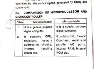
  • 1. controlled by the control signals generated by timing and control unit. 2.7. COMPARISON OF MICROPROCESSOR AND MICROCONTROLLER Microcontroller S.No Microprocessor 1. It is a general purpose It is a special purpose 1 digital computer. digital computer. It contains CPU, It contains CPU, Timers/ memory| Counters, serial and addressing circuits,parallel 1/0 ports, handlingInternal RAM, Internal ROM etc., 2. registers, interrupt circuits etc.,
  • 2. 2.08 3. It has many op-codes | It has one or two op-codes for moving 3. for moving data from extenal memory to the data from external| CPU. memory to the CPU. It has one or two bit handling instructions. It has many bit handling instructions. To function as computer, 4. To function as computer, 5 it needs additional it does not need any external parts. external parts. 6 Examples: 8085,8086, Exampes: 8051,8048, Z80 etc. 8052 etc., 2.8.SIGNAL DESCRIPTION OF 8051 PLO 40cc PI.I2 39 PO.0/ADO P1.2 3 38PO.1/ADI 37P0.2/AD2 36P0.3/AD3 P13 4 P14 5 PI.5 6 P16 7 35PO4/AD4 34 P0.5/AD5 P1.7 8 RESET9 (RXD)P3.010 IC 8051 31 EAVPP 33PO.6/AD6 32PO.7/AD7 TXD)P3.1 30AL.E/PROG INTO)P3.2 12 INTT)P3.3 13 29 PSEN 28 P2.7/A15 (TOP34 14 (TI)P3.5 15 (WRP3.6 16 27P2.6/A14 26P2.5/A13 25 P2.4/A12 (RD)P3.7 7 XTAL2 18 XTALI 19 s 20 24P2.3/A11 23P2.2/A10 22P2.1/A9 21P2.0/A8 Fig. 2.2 Pindiagram of 8051
  • 3. 2.09 M i c r o c o n t r o l l e r 8051 is a v a i l a b l e in a 40 pin plastin ceramic DIP p a c k a g e s . The pin diagram of8051 is shou a 40 pin plastic and 1 is show in the fig.2.2. b ) V s s : It is a return pin for the supply (Ground). b) ) V o c : It is a +5Vsupply voltage pin. a) to reset the c) m i c r o c o n t r o l l e r . RESET: The reset pin is used to reset the e d indicates that the valid address bits are available their respective pins. This ALE signal is valid only for external memory accesses. This pin also act as program pulse input during on-chip EPROM programming. d)ALE/PROG:Theaddress latch enable output pulse on e) EAVpp: External access pin, iftied low, indicates that the 8051 can address external program memory. For execution of programs in internal program memory this pin must be tied high. This pin also receives 21 Voits for programming the on-chip EPROM. PSEN: This program store enable pin is not activated for internal fetches. It is activated when the CPU IS accessing external program memory. PSEN I activated twice every cycle. g) Port0 (PO.0 P0.7): Port 0 acts as an 8" bidirectional bit/byte addressable /O port. This ra as been allotted an address in the SFR address rany range (ADa-AD) during external memory access. also receives code bytes during programming Port 0 acts as multiplexed address and data i R address ess and data line: 0 internal EPROM. the
  • 4. h) Port 1(P1.0 - P1.7): Port 1 acts as an 8-bit h) bidirectional bit/byte addressable port. It has been allotted an address in the SFR address range. i)Port 2 (P2.0 P2.7): Port2 acts as 8-bit bidirectional bitbyte addressable l/O port. It has been allotted an address in the SFR address range. During external memory access, port 2 emits higher eight bits of address (As - A15). Port 2 also receives higher order address bits during programming on the on-chip EPROM. Port 3 (P3.0- P3.7): Port 3 is an 8-bit bidirectional bit/ byte addressable l/0 port. It has been allotted an address in the SFR address range. The port 3 pins also serve the alternate functions as listed in the table below. Port Pins Alternate Functions P3.0 RXD (Serialinputport) P3.1 TXD (Serial output port) P3.2 INTO (External interrupt 0) P3.3 INT1. (External interrupt 1) P3.4 TO (Timer/Counter0 external input) P3.5 T1 (Timer/Counter 1 external input) P3.6 WR (External data memory write strobe) P3.7 RD (External data memory read strobe)
  • 5. 2.11 XTALI and XTAL2 There is an in-built oscillato. which derives the necessary clock frequency for tha operation of the oscillator. XTAL1 is the input to the inverting oscillator amplifier. XTAL2 is the output from the inverting oscillator amplifier. ALLL (ARITHMETIOAND LOCIR IAITV
  • 6. Spaces. 2.11.1. ROM (Program memory) Program memory can only be read, not written to. There can be upto 64 Kbytes of program memory. In the ROM and EPROM versions, the lowest 4 Kbytes are provided on-chip. In the ROM less versions all program memory is external (off-chip). The 64 Kbyte program memoiy
  • 7. 2.14 space consists of an internal and external memory portions. The memory map structure of program memory is shown in the fig. 2.3. In microcontroller 8051, the lower 4 Kbytes of program memory can be placed either in the on-chip ROM or in an external ROM. This selection is made by strapping the EA pin to either Vcc or Vss. If the EA pin is held high, the program fetches to addresses 0000H through OFFFH are directed to the internal ROM. Program fetches to addresses 1000H through FFFFH are directed to the external ROM. FFFF EXTERNAAL EA -0 or1 1000L OFFF OFFF EXTERNAL (EA=0) INTERNAL CEA = 1) Fig. 2.3 Memory map of program memory If the EA pin is held low, the microcontroller 8051 etches all instructions from external program memory. The read strobe to external ROM, PSEN is used for all program fetches. PSEN is not activated for internal program fetches. Locations 00 through 23H in program memory are used by interrupt service routine.
  • 8. 2.15 The data memory address space consists ns memory The 2.11.2. RAM (Data memory) of an internal and external memory spaces. External datamer is accessed, when a MOVX i n s t r u c t i o n is executed structure of data memory is shown in the fig.2.4. FFFFU INTERNAL DATA MEMORY EXTERNAL DATA MEMORY FFH SPECIAL (64 Kby tes) FUNCTION RECISTER 128 bytes sOH 7FH INTERNAL DATA RAM 128 bytes 00L1 0000H Fig.2.4 Memory, map ofdata memory Internal data memory is divided into two physically separate and distinct blocks. They are, i) The lower 128 bytes of RAM (internal RAM) area, and i) The upper 128 bytes of special function register (RAM) area The address range of internal RAM is from 00H to 7FH, and the address range of SFR is from 80H and FFH. The structure of internal data memory space is sno n in the fig.2.5. Four 8-bit register banks occupy locations through 31 in lower RAM area. Only one of these banks may
  • 9. 2.16 he enabled at a time, through a two bit field in PSW. The next 16-bytes, locations 32 through 47 contain 128 bit addressable locations. Again the next 80 bytes, locations 48 through 127 contain only byte addressable locations. The SFR area also has byte and bit addressable locations. Internal data memory addresses are always one byte wide. All the bytes in the lower 128 can be accessed by either direct or indirect addressing. The SFRs are accessed by only direct addressing. 255 FOH EOH DOH- B8H Special function BOH ADDRESABLE BITS IN SFRs registers A8H AOH 98H 90H 88H 128 80H 127 48 128 120 ADDRESABLE BITS IN RAM 32 7 (128 BITS) R BANK 3 24 R R1 INTERNAL BANK 2 DATA RAM 16 REGISTERS R BANK1 8 R R BANK R Fig. 2.5 Structure of internal data memory space
  • 10. 2.17 The CPU generates RD and WR signals as needed during external RAM accesses. There can be up to 64 Kbytes of external data memory. Memory addresses can be either 1 or 2 bytes wide. Only indirect addressing can be used for accessing external data memory. In one byte addresses, the location is indirectly specified either in register R0 or R1, which is specified as @Ri. In two byte addresses, the location is indirectly specified in register DPTR, specified as @DPTR. In all external data RAM accesses, the accumulator is always the destination or source of the data. The external RAM IS activated only during the execution of a MOVX instruction. 2.11.3. Internal RAM memory map 7F Only byte
  • 11. 3.05 34. ADDRESSING MODES The ways by which the addresses are specified in the struction are called addressing modes. Generally, the data sters or emory. But we can call for accessing the data in different modes. Hence the ways of accessingdata are required reQuired for manipulating instructions are either placed in called addressing modes. The microcontroller 8051 provides five addressing modes. Theyare a) Immediate addressing b) Direct addressing Indirect addressing d) Register addressing e) Index addressing a) Immediate addressing mode In this mode of addressing, an immediate data i.e. a constant is specified in the operand field. By using this addressing mode, we can move immediate data and also doing arithmetic and logical operations with immediate data. All immediate data are proceded by a hash (#) symbol. Example MOV A, #64H This instruction loads the A c c u m u l a t o r with the hexadecimal data of 64H. b) Register addressing mode In this mode of addressing, operands are stored in registers from RO to R7 of the s e l e c t e d register bank: the
  • 12. 3.06 When the instruction is executed, one of the eight registersin the selocted register bank is accessed. One of the four banks selec bits in the PSW register. The least significant three bito to be used, is selected at the execution time by using the two ba bits of the instruction op-code indicate which register is to be Acc B, DPTR and CY (boolean process accumulator) can also be addressed as registers. Example: MOV A, R3 This instruction moves the data from register R3 into Accumulator. c) Direct addressing Mode In this mode of addressing, the operand is specified by an 8-bit address field in the instruction format. Only internal data RAM(lower 128 bytes) and special function registers can be directly addressed. Example: MOV direct, A This instruction moves the content of accumulator of accumulator to direct address directly. NOTE: Direct is the address of either lower 128 byi lower 128 byte internal data memory or special function regis inction register. d) Indirect addressing mode In this mode of addressing, the instructi a ction specifie register which contains the address of the operand. Both internal and external RAM can be addressed indirectily.
  • 13. 3.07 address register for 8-6it address can be RO or oftheselec of thister for 16-bit address can only be the 16-bit ected register bank, or the stack pointer. The d a t ap o i n t e r ( D P T R ) . oE& bytes of external data memory can be specified The address of 128 bytes of internal RAM and the dóress space is accomplished using the 16-bit DPTR. The ress register for lower2 5 6 in register Ro 1. The full 64 Kbytes data memory cial function registers are not to be accessed by this method. Execution of PUSH and POP instructions also uses register-indirect addressing. Example: a)MOVR1, A This instruction moves the coutent of Acc to the internal RAM location, specified by the register R1. b) MOVX A, @DPTR This instruction moves the content of external RAM memory location specified by DPTR to Acc. e) Index addressing mode Index addressing mode is otherwise called as base egister plus index register indirect addressing intended for reading look-up table in program memory. COunter) points to the base of the table and the Accumulator Arde..ny program memory can be accessed with index addressing, ining, and it can only be read. This addressing mode is A 16-bit base register (either DPTR or the program
  • 14. 3.08 ress of the table is setup with the table entry number. The address of th entry in program memory is formed by adding the conte of Accumulator and the base register. In the case of jump instructions, the content Accumulator is added with one ot the specified 18 of 6-bit registers to form the jump destination address. Example: a) MOVCA, @A+DPTR The content of program memory, which address is specified by the sum of the contents of the registers A and DPTR is moved into Accumulator. b)JMP@A+DPTR The control of microcontroller is transferred to the memory location, which is the sum of the addresses specified by Accumulator and DPTR. Actually the sum of the contents of Accumulator and DPTR is loaded into the program counter. 3.5. DATA TRANSFER INSTRUCTIONs Data transfer instructions are divided into three classes. They are, a) General purpose instructions b) Accumulator specific instructions, and c) Address- object instructions. a) General purpose data transfer instructions There are 3 major types of instructions u used for transferring data in general purpose.
  • 15. IS moved Trom one place to anotner place. Except a iS moved Trom one place to another place. cept a POP PSW or MOV directly to the PSW instruction, the conditional flag settings are not affected. do ho> he byte level data transfer instructions are described belownStruc 1) MOV A, Rn (Move register to Accumulator) S (A) (Rn) The content of the register Rn is copied into the Accumulator 2) MOV A, direct.(Move direct byte to Accumulator) (A) (direct)
  • 16. 3.10 The content of directly addressed location is copied into the Accumulator. 3) MOV A. @Ri (Move indirect RAM to Accumulatol ((Ri) ator) (A) The content of memory location, which is ddressed by the register Ri is copied in to the Accumulato. Accumulato 4) MOV A, #data (Move immediate data to the Accumula (A) #data The content of second byte of the instruction is copied into the Accumulator 5) MOV Rn. A (Move Accumulator to register) (Rn) (A) The content of accumulator is copied into the register Rn. 6) MOV Rn, direct (Move direct byte to Register) (Rn) (direct) The content of directly addressed location is copie0 into register Rn. 7) MOV Rn, #data (Move immediate data to register) (Rn) #data is The content of the second byte of the instrucio copied into the register Rn. 8) MOV direct, A (Move Accumulator to direct byte) (direct) (A) The content of Accumulator is copied into the directly specified location.
  • 17. 3.11 MOVdirect, Rn (Move register to direct byte) (direct) (Rn) The content of register Rn is copied into the directly specified location. MOV direct, direct (Move direct byte to direct byte) (direct) (direct) The content of location directly specified in the source ocerand is copied into another directly specified location ir ne destination operand. 11) MOV direct, @Ri (direct) (R) The content of memory location, which is addressed by the register Ri is copied in to the directly specified location. 12) MOV direct, #data (direct) #data The content of third byte of the instruction is copied in to the directly specified location. 13) MOV @Ri, A (Move Accumulator to indirect RAM) ((Ri)) (A) The content of Accumulator is copied into the internal AM memory location, which address is specified in the egister Ri. 4) MOV @Ri, direct (Move direct byte to indirect RAM) ((Ri)) (direct)
  • 18. 3.12 The content of directly specified location is copied into internal RAM location, which address is specified in the register Ri (RO or R1) 15) MOV @Ri, #data (Move immediate data to indirect RAM) ((Ri)) #data The content of second byte of the instruction is The copied into internal RAM location, which address is specified in the register Ri (RO or R1)