
Recommended
More Related Content
What's hot
What's hot (20)
Similar to IC-741 (Op-Amp)
Similar to IC-741 (Op-Amp) (20)
Recently uploaded
Recently uploaded (20)
IC-741 (Op-Amp)
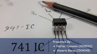
- 1. 741 IC Presented By: ● Nafisa Tasneem (1509032) ● Showrin Barua (1509048)
- 2. Introduction • An integrated circuit is a semiconductor wafer on which thousands or millions of tiny resistors, capacitors and transistors are fabricated. • IC-741 is most commonly used which is an Operational Amplifier. 625 Million Transistors 2
- 3. History • The IC-741 was designed by Dave Fullager of Fairchild Semiconductor in 1968. Genius Creation 3
- 4. Pin Diagram 1Offset Null 5 Offset Null The Offset Null pins are used for adjusting offset voltage to obtain better gain 4
- 5. Pin Diagram 1Offset Null 5 Offset Null This pin is used to invert the input voltage at 180° 2Inverting In 4
- 6. Pin Diagram 1Offset Null 5 Offset Null This pin does not change the polarity of the given input voltage 2Inverting In 3Non Inverting In 4
- 7. Pin Diagram 1Offset Null 5 Offset Null These pins are used for positive and negative supply to the IC 2Inverting In 3Non Inverting In 4-Vcc 7 +Vcc 4
- 8. Pin Diagram 1Offset Null 5 Offset Null This pin is used for taking output of the IC 2Inverting In 3Non Inverting In 4-Vcc 7 +Vcc 6 Output 4
- 9. Pin Diagram 1Offset Null 5 Offset Null 2Inverting In 3Non Inverting In 4-Vcc 7 +Vcc 6 Output 8 Not Connected 4
- 10. Other Types of 741 IC 5
- 11. Maximum Ratings Supply voltage ±18 𝑣𝑜𝑙𝑡𝑠 Internal power dissipation 500mW Differential input voltage ±30 𝑣𝑜𝑙𝑡𝑠 Input voltage ±15 𝑣𝑜𝑙𝑡𝑠 Voltage offset null/V- ±0.5 𝑣𝑜𝑙𝑡𝑠 Operating temperature range 0° to +70°C Storage temperature range -65° to +150°C Lead temperature 300°C Output short circuit Indefinite 6
- 12. Block Diagram Input stage Intermediate stage Level shifting stage Output stage + - o/p i/p This stage provides most of the voltage gain of the op-amp and establishes its input resistance 7
- 13. Block Diagram Input stage Intermediate stage Level shifting stage Output stage + - o/p i/p This stage uses unbalanced differential amplifier for direct coupling. At the output of this stage DC voltage is above ZERO 7
- 14. Block Diagram Input stage Intermediate stage Level shifting stage Output stage + - o/p i/p This stage uses level translator circuit. It makes the DC voltage downward to ZERO with respect to ground. 7
- 15. Block Diagram Input stage Intermediate stage Level shifting stage Output stage + - o/p i/p This stage uses complementary push-pull amplifier. It increases the output voltage swing and raises current supplying capability of the op-amp. It also establishes low output impedance. 7
- 16. Important Specifications i. Input offset voltage ii. Input offset current iii.Input bias current iv.Slew rate v. CMRR (Common mode rejection ratio) 8
- 17. Important Specifications i. Input offset voltage : It is the voltage that must be applied between the two input terminals of an op-amp to null the output voltage. Vio = Vdc1 – Vdc2 9
- 18. Important Specifications ii. Input offset current : It is the algebraic difference of two input currents that flow into the inverting and non-inverting terminals of an op-amp. Iio = | IB1 – IB2 | 10
- 19. Important Specifications iii. Input bias current : It is the average of two input currents that flow into the inverting terminal of an op-amp. IB = (IB1 + IB2) / 2 11
- 20. Important Specifications iv. Slew rate: It is defined as the maximum change of output voltage per unit time and expressed as v/μs. SR = 𝑑𝑉0 𝑑𝑡 |max 12
- 21. Important Specifications v. CMRR: Common mode rejection ratio is generally defined as the ratio of differential voltage gain (Ad) to the common mode voltage gain (Acm). CMRR = 𝐴 𝑑 𝐴 𝑐𝑚 & Acm = 𝑉 𝑜𝑐𝑚 𝑉 𝑐𝑚 13
- 22. Important Features i. Short circuit and overload protection provided. ii. Low power consumption. iii. Large common mode rejection ratio (CMRR) and differential voltage ranges. iv. No external frequency compensation is required v. No latch-up problem. 14
- 23. Important Applications (1/4) Headphone Amplifier 15
- 27. Future We have seen that many sectors have been developed using IC 741. As we are future electronics engineers, the future of IC 741 as well as other electronic devices depend on us. So it is our responsibility to think something different . Who knows it (IC 741) may create a new dimension in modern electronics! 19
- 28. References i. Op-amps and linear integrated circuits - Ramakant A. Gayakward ii. Ctcircuitstoday.com iii. Quora.com iv. Electroschematics.com 20
- 29. THANK YOU