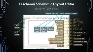
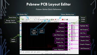
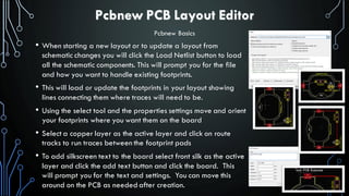
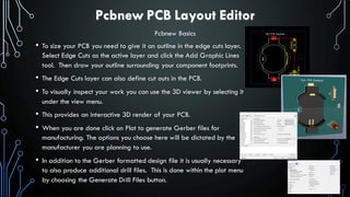
PCB Design
with the
KiCad EDA
PRESENTED BY RICHARD GOWEN (@alt_bier)
Created for BSidesDFW 2020 HHV
This Slide Deck Is Available at https://altbier.us/pcb/
What are all these acronyms?
• PCB = Printed Circuit Board
• A PCB mechanically supports and electrically connects electronic components using
conductive tracks and pads that are etched from copper laminated on sheets of a non-
conductive substrate. The pattern is etched using a form of photolithography allowing
mass duplication like photographs from a film negative thus ‘printing’ the circuit boards.
• EDA = Electronic Design Automation
• A category of software tools for designing electronic systems such as integrated circuits
and printed circuit boards.
• KiCad = “Ki” + Computer Aided Design
• The term ‘Ki’ (pronounced Key even though I keep saying it wrong) is a reference to a
company that the original software author Jean-Pierre Charras knew.
• Computer Aided Design refers to the use of computers in the creation, modification,
analysis, or optimization of a design.
• KiCad is an open source software suite for electronic design automation.
KiCad Overview
KiCad is an open source software suite for EDA that has the following features:
• A Schematic editor to create your design.
• It comes with a stocked library of schematic symbols but also includes a schematic
symbol editor to modify or create your own
• A PCB Layout editor supporting up to 32 copper layers with auto-routing options.
• It comes with a stocked library of PCB footprints but also includes a footprint editor to
modify or create your own
• A 3D Viewer which allows you to inspect your design in an interactive canvas.
• It comes with a stocked library of 3D models and includes options to easily import
additional 3D models as needed and tie them to footprints.
• These three features being linked together with reference points between symbols
and footprints and models allows for ease of design with quick visual confirmation
• You can download the program and find libraries and documentation here:
https://kicad-pcb.org/
Project File Layout
KiCad will create files in a project directory when you work with various features.
Here is a list of those files and a recommended directory structure to use for organization.
• < project name >.pro – the main project file.
Holds parameters that apply to the entire project (e.g. schematic, PCB layout, etc.).
• < project name >.sch – a schematic file.
• < project name >.kicad_pcb - a PCB New layout file.
• < project name >.net – netlist in "Pcbnew" format
• < project name >.bak – backup of schematic file.
• < project name >.kicad_pcb-bak – backup of the new PCB layout file.
• < project name >-cache.lib – a local cache copy of all the symbols used in the schematic
• < project name >-kicad_wks – page layout worksheet template file
• fp-lib-table – Footprint library list
• sym-lib-table – Schematic library list
• ./3d_models/ – Optional directory contains local 3d model files
• ./gerber/ – Optional directory contains gerber formatted output files for manufacturing
• ./lib_fp/ – Optional directory contains local footprint module directories
• ./lib_sh/ – Optional directory contains local schematic library files
• ./snapshots/ – Optional directory contains prints of schematic / cad files and images
Setting Project Preferences
You will want to review some default project
setting and adjust them as needed.
• Configure Paths allows you to set which
directories will be searched for files
• Manage Symbol Libraries allows you to set
which global libraries will be available to
your project and the location of local project
specific libraries (e.g. /lib_sh/local.lib)
• Manage Footprint Libraries allows you to set
which global libraries will be available to
your project and the location of local project
specific libraries (e.g. /lib_fp/local.pretty)
KiCad Program Layout
The program layout is intuitive and easy to navigate.
Schematic
Layout
Editor
Eeschema
Symbol
Editor
PCB
Layout
Editor
Pcbnew
Footprint
Editor
Gerber
File
Viewer
GerbView
Bitmap
Converter
Project
File
Explorer
PCB &
Component
Calculator
Page Layout
Editor
KiCad Design Workflow
• Open Eeschema to create a schematic
• Use the symbol editor as needed to create or modify symbols
• Use the calculator as needed to verify component values.
• Associate component symbols with footprints
• Use the footprint editor if needed to create or modify footprints
• Generate a Netlist file from Eeschema
• Open Pcbnew to layout the PCB
• Import the Netlist file
• Size the board, move components around, run traces, add vias, etc.
• Use the calculator as needed to verify track widths and spacing.
• Associate component footprints with 3D models if needed
• Use the 3D viewer to visually inspect your work.
• Plot gerber files from Pcbnew for manufacturing
• Open GerbView to confirm the integrity of the Gerber files
• Send Gerber files to manufacturer
Eeschema Schematic Layout Editor
Eeschema Button Quick Reference
Page
Settings
Select
Place Symbol
Place Wire
Wire to Bus
No Connection Flag
Net Label
Hierarchical Label
Hierarchical Pin Import
Graphic Lines
Highlight Net
Power Port
Place Bus
Bus to Bus
Junction
Option
Toggles
Global Label
Create Hierarchical Sheet
Create Hierarchical Pin
Place Text
Open
Footprint
Editor
Open
Symbol
Editor
Generate
Netlist
Assign Footprints to Symbols
Electrical Rules Check
Eeschema Schematic Layout Editor
• To place a new symbol on your schematic click the Place
Symbol tool and click on the schematic page. You will be
prompted to choose a symbol from the available libraries.
• To move or rotate a placed symbol right-click it and
choose the move or orientation menus
• To connect symbols choose the wire or bus tool and select
the symbol pins to connect.
• To edit a symbol reference number double-click on it
• To edit all the properties of a symbol right click and
choose the Edit Properties menu
Eeschema Basics
Eeschema Schematic Layout Editor
• To add additional information to a symbol under edit
properties click the + add field and enter your text and choose
if it should be shown.
• To place a label click the global label tool and click on the
schematic. You will be prompted enter the label and other
setting like orientation.
• Global labels can be used to connect wire nets without crossing
wires on the schematic.
• Make sure that all your symbols have associated footprints by
clicking the Assign Footprints button and selecting footprints for
the symbols that need them.
• When complete click the Generate Netlist button to create the
file that will be imported into Pcbnew
Eeschema Basics
Symbol Editor
The Symbol Editor works much like the Eeschema Schematic Layout Editor. The major
difference being that you are working with one symbol in a library at a time.
You can copy symbols to have variations of text or footprint assignments.
These symbols are stored in the libraries that are available for use by Eeschema.
Pcbnew PCB Layout Editor
Pcbnew Button Quick Reference
Change Track &
Via & Grid Settings
Select
Option
Toggles
Open
Footprint
Editor
Load
Netlist
Choose Working Layer
Plot Gerber Files
Board Setup
Highlight Net
Ratsnest
Add Footprint
Route Tracks
Add Vias
Add Filled Zones
Choose
Visible
Layers
Keepout Areas
Graphic Lines
Graphic Arc
Graphic Circle
Graphic Polygon
Add Text
Add Dimension
Layer Alignment
Pcbnew PCB Layout Editor
• When starting a new layout or to update a layout from
schematic changes you will click the Load Netlist button to load
all the schematic components. This will prompt you for the file
and how you want to handle existing footprints.
• This will load or update the footprints in your layout showing
lines connecting them where traces will need to be.
• Using the select tool and the properties settings move and orient
your footprints where you want them on the board
• Select a copper layer as the active layer and click on route
tracks to run traces between the footprint pads
• To add silkscreen text to the board select front silk as the active
layer and click the add text button and click the board. This
will prompt you for the text and settings. You can move this
around on the PCB as needed after creation.
Pcbnew Basics
Pcbnew PCB Layout Editor
• To size your PCB you need to give it an outline in the edge cuts layer.
Select Edge Cuts as the active layer and click the Add Graphic Lines
tool. Then draw your outline surrounding your component footprints.
• The Edge Cuts layer can also define cut outs in the PCB.
• To visually inspect your work you can use the 3D viewer by selecting it
under the view menu.
• This provides an interactive 3D render of your PCB.
• When you are done click on Plot to generate Gerber files for
manufacturing. The options you choose here will be dictated by the
manufacturer you are planning to use.
• In addition to the Gerber formatted design file it is usually necessary
to also produce additional drill files. This is done within the plot menu
by choosing the Generate Drill Files button.
Pcbnew Basics
Footprint Editor
The Footprint Editor works much like the Pcbnew PCB Layout Editor. The major difference
being that you are working with one footprint in a library at a time.
You can copy footprints to have variations of text or 3D model assignments.
These footprints are stored in the libraries that are available for use by Pcbnew.
Gerber File Viewer
The Gerber File Viewer lets you load Gerber formatted design files for viewing.
These can be files you have created or from a project you downloaded.
There is a separate Gerber file for each layer of the design. You can open multiple files
at once to overlay the entire PCB design.
Bitmap to Component Converter
This tool takes a bitmap image to generate a footprint file.
This can be a handy way to import a logo to your silkscreen layer.
It’s also good for complex fill areas or edge cuts created in an art program.
PCB Calculator
This tool bundles several useful calculation and reference items.
Page Layout Editor
This tool allows you to change the default look of the printed design pages.
PCB Manufacturing
Once you have completed your design you are ready to send it to be manufactured.
There are several factors to consider when choosing a PCB manufacturer. Cost is probably
the top factor. But time and location and quality are all also important. The cheapest PCB
manufacturer might take months to deliver or might have poor quality.
Look at customer reviews and do some small prototype runs to confirm they meet your
needs. There are many PCB manufacturers to choose from.
Here are a few:
• https://pcbshopper.com/ Travelocity like site for PCB Mfrs.
• https://jlcpcb.com/ Very Inexpensive but with some limitations.
• https://pcbway.com/ Inexpensive and fast shipping.
• https://oshpark.com/ Beautiful, High Quality, made in USA
THANK YOU
I hope you enjoyed this presentation and learned something from it.
-- @alt_bier
This Slide Deck – https://altbier.us/pcb/
Code – https://github.com/gowenrw/BSidesDFW_2020_HHV/

PCB Design with KiCad.pdf

  • 1.
    PCB Design with the KiCadEDA PRESENTED BY RICHARD GOWEN (@alt_bier) Created for BSidesDFW 2020 HHV This Slide Deck Is Available at https://altbier.us/pcb/
  • 2.
    What are allthese acronyms? • PCB = Printed Circuit Board • A PCB mechanically supports and electrically connects electronic components using conductive tracks and pads that are etched from copper laminated on sheets of a non- conductive substrate. The pattern is etched using a form of photolithography allowing mass duplication like photographs from a film negative thus ‘printing’ the circuit boards. • EDA = Electronic Design Automation • A category of software tools for designing electronic systems such as integrated circuits and printed circuit boards. • KiCad = “Ki” + Computer Aided Design • The term ‘Ki’ (pronounced Key even though I keep saying it wrong) is a reference to a company that the original software author Jean-Pierre Charras knew. • Computer Aided Design refers to the use of computers in the creation, modification, analysis, or optimization of a design. • KiCad is an open source software suite for electronic design automation.
  • 3.
    KiCad Overview KiCad isan open source software suite for EDA that has the following features: • A Schematic editor to create your design. • It comes with a stocked library of schematic symbols but also includes a schematic symbol editor to modify or create your own • A PCB Layout editor supporting up to 32 copper layers with auto-routing options. • It comes with a stocked library of PCB footprints but also includes a footprint editor to modify or create your own • A 3D Viewer which allows you to inspect your design in an interactive canvas. • It comes with a stocked library of 3D models and includes options to easily import additional 3D models as needed and tie them to footprints. • These three features being linked together with reference points between symbols and footprints and models allows for ease of design with quick visual confirmation • You can download the program and find libraries and documentation here: https://kicad-pcb.org/
  • 4.
    Project File Layout KiCadwill create files in a project directory when you work with various features. Here is a list of those files and a recommended directory structure to use for organization. • < project name >.pro – the main project file. Holds parameters that apply to the entire project (e.g. schematic, PCB layout, etc.). • < project name >.sch – a schematic file. • < project name >.kicad_pcb - a PCB New layout file. • < project name >.net – netlist in "Pcbnew" format • < project name >.bak – backup of schematic file. • < project name >.kicad_pcb-bak – backup of the new PCB layout file. • < project name >-cache.lib – a local cache copy of all the symbols used in the schematic • < project name >-kicad_wks – page layout worksheet template file • fp-lib-table – Footprint library list • sym-lib-table – Schematic library list • ./3d_models/ – Optional directory contains local 3d model files • ./gerber/ – Optional directory contains gerber formatted output files for manufacturing • ./lib_fp/ – Optional directory contains local footprint module directories • ./lib_sh/ – Optional directory contains local schematic library files • ./snapshots/ – Optional directory contains prints of schematic / cad files and images
  • 5.
    Setting Project Preferences Youwill want to review some default project setting and adjust them as needed. • Configure Paths allows you to set which directories will be searched for files • Manage Symbol Libraries allows you to set which global libraries will be available to your project and the location of local project specific libraries (e.g. /lib_sh/local.lib) • Manage Footprint Libraries allows you to set which global libraries will be available to your project and the location of local project specific libraries (e.g. /lib_fp/local.pretty)
  • 6.
    KiCad Program Layout Theprogram layout is intuitive and easy to navigate. Schematic Layout Editor Eeschema Symbol Editor PCB Layout Editor Pcbnew Footprint Editor Gerber File Viewer GerbView Bitmap Converter Project File Explorer PCB & Component Calculator Page Layout Editor
  • 7.
    KiCad Design Workflow •Open Eeschema to create a schematic • Use the symbol editor as needed to create or modify symbols • Use the calculator as needed to verify component values. • Associate component symbols with footprints • Use the footprint editor if needed to create or modify footprints • Generate a Netlist file from Eeschema • Open Pcbnew to layout the PCB • Import the Netlist file • Size the board, move components around, run traces, add vias, etc. • Use the calculator as needed to verify track widths and spacing. • Associate component footprints with 3D models if needed • Use the 3D viewer to visually inspect your work. • Plot gerber files from Pcbnew for manufacturing • Open GerbView to confirm the integrity of the Gerber files • Send Gerber files to manufacturer
  • 8.
    Eeschema Schematic LayoutEditor Eeschema Button Quick Reference Page Settings Select Place Symbol Place Wire Wire to Bus No Connection Flag Net Label Hierarchical Label Hierarchical Pin Import Graphic Lines Highlight Net Power Port Place Bus Bus to Bus Junction Option Toggles Global Label Create Hierarchical Sheet Create Hierarchical Pin Place Text Open Footprint Editor Open Symbol Editor Generate Netlist Assign Footprints to Symbols Electrical Rules Check
  • 9.
    Eeschema Schematic LayoutEditor • To place a new symbol on your schematic click the Place Symbol tool and click on the schematic page. You will be prompted to choose a symbol from the available libraries. • To move or rotate a placed symbol right-click it and choose the move or orientation menus • To connect symbols choose the wire or bus tool and select the symbol pins to connect. • To edit a symbol reference number double-click on it • To edit all the properties of a symbol right click and choose the Edit Properties menu Eeschema Basics
  • 10.
    Eeschema Schematic LayoutEditor • To add additional information to a symbol under edit properties click the + add field and enter your text and choose if it should be shown. • To place a label click the global label tool and click on the schematic. You will be prompted enter the label and other setting like orientation. • Global labels can be used to connect wire nets without crossing wires on the schematic. • Make sure that all your symbols have associated footprints by clicking the Assign Footprints button and selecting footprints for the symbols that need them. • When complete click the Generate Netlist button to create the file that will be imported into Pcbnew Eeschema Basics
  • 11.
    Symbol Editor The SymbolEditor works much like the Eeschema Schematic Layout Editor. The major difference being that you are working with one symbol in a library at a time. You can copy symbols to have variations of text or footprint assignments. These symbols are stored in the libraries that are available for use by Eeschema.
  • 12.
    Pcbnew PCB LayoutEditor Pcbnew Button Quick Reference Change Track & Via & Grid Settings Select Option Toggles Open Footprint Editor Load Netlist Choose Working Layer Plot Gerber Files Board Setup Highlight Net Ratsnest Add Footprint Route Tracks Add Vias Add Filled Zones Choose Visible Layers Keepout Areas Graphic Lines Graphic Arc Graphic Circle Graphic Polygon Add Text Add Dimension Layer Alignment
  • 13.
    Pcbnew PCB LayoutEditor • When starting a new layout or to update a layout from schematic changes you will click the Load Netlist button to load all the schematic components. This will prompt you for the file and how you want to handle existing footprints. • This will load or update the footprints in your layout showing lines connecting them where traces will need to be. • Using the select tool and the properties settings move and orient your footprints where you want them on the board • Select a copper layer as the active layer and click on route tracks to run traces between the footprint pads • To add silkscreen text to the board select front silk as the active layer and click the add text button and click the board. This will prompt you for the text and settings. You can move this around on the PCB as needed after creation. Pcbnew Basics
  • 14.
    Pcbnew PCB LayoutEditor • To size your PCB you need to give it an outline in the edge cuts layer. Select Edge Cuts as the active layer and click the Add Graphic Lines tool. Then draw your outline surrounding your component footprints. • The Edge Cuts layer can also define cut outs in the PCB. • To visually inspect your work you can use the 3D viewer by selecting it under the view menu. • This provides an interactive 3D render of your PCB. • When you are done click on Plot to generate Gerber files for manufacturing. The options you choose here will be dictated by the manufacturer you are planning to use. • In addition to the Gerber formatted design file it is usually necessary to also produce additional drill files. This is done within the plot menu by choosing the Generate Drill Files button. Pcbnew Basics
  • 15.
    Footprint Editor The FootprintEditor works much like the Pcbnew PCB Layout Editor. The major difference being that you are working with one footprint in a library at a time. You can copy footprints to have variations of text or 3D model assignments. These footprints are stored in the libraries that are available for use by Pcbnew.
  • 16.
    Gerber File Viewer TheGerber File Viewer lets you load Gerber formatted design files for viewing. These can be files you have created or from a project you downloaded. There is a separate Gerber file for each layer of the design. You can open multiple files at once to overlay the entire PCB design.
  • 17.
    Bitmap to ComponentConverter This tool takes a bitmap image to generate a footprint file. This can be a handy way to import a logo to your silkscreen layer. It’s also good for complex fill areas or edge cuts created in an art program.
  • 18.
    PCB Calculator This toolbundles several useful calculation and reference items.
  • 19.
    Page Layout Editor Thistool allows you to change the default look of the printed design pages.
  • 20.
    PCB Manufacturing Once youhave completed your design you are ready to send it to be manufactured. There are several factors to consider when choosing a PCB manufacturer. Cost is probably the top factor. But time and location and quality are all also important. The cheapest PCB manufacturer might take months to deliver or might have poor quality. Look at customer reviews and do some small prototype runs to confirm they meet your needs. There are many PCB manufacturers to choose from. Here are a few: • https://pcbshopper.com/ Travelocity like site for PCB Mfrs. • https://jlcpcb.com/ Very Inexpensive but with some limitations. • https://pcbway.com/ Inexpensive and fast shipping. • https://oshpark.com/ Beautiful, High Quality, made in USA
  • 21.
    THANK YOU I hopeyou enjoyed this presentation and learned something from it. -- @alt_bier This Slide Deck – https://altbier.us/pcb/ Code – https://github.com/gowenrw/BSidesDFW_2020_HHV/