The document discusses registers and counters in clocked sequential circuits, focusing on their functions and constructions, particularly with flip-flops. It describes different types of registers, such as shift registers and bcd counters, along with their operational mechanisms including parallel and serial data transfers. Additionally, it covers universal shift registers, ripple counters, and synchronous counters, explaining their applications in digital systems.


![12
Serial Transfer
n To prevent the loss of information stored in
the source register, the information in
register A is made to circulate by connecting
the serial output to its serial input.
n The shift control input determines when and
how many times the registers are shifted.
This is done with an AND gate that allows
clock pulses to pass into the CLK terminals
only when the shift control is active. [Fig. 6-
4(a)].](https://image.slidesharecdn.com/sequentialcircuits-240209052844-4873578e/85/Sequential-circuits-Sequential-circuits1-12-320.jpg)


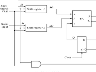
![17
Serial Addition
n Operations in digital computers are usually
done in parallel because this is a faster
mode of operation.
n Serial operations are slower, but have the
advantage of requiring less equipment.
n The two binary numbers to be added serially
are stored in two shift registers.
n Bits are added one pair at a time through a
single full adder. [Fig. 6-5]](https://image.slidesharecdn.com/sequentialcircuits-240209052844-4873578e/85/Sequential-circuits-Sequential-circuits1-17-320.jpg)

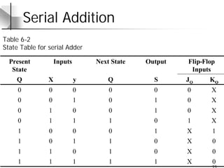
![20
Serial Addition
n To show that serial operations can be
designed by means of sequential circuit
procedure, we will redesign the serial adder
using a state table.
n The serial outputs from registers are
designated by x and y.
n The sequential circuit proper has two inputs,
x and y, that provide a pair of significant bits,
an output S that generates the sum bit, and
flip-flop Q for storing the carry. [Table. 6-2]](https://image.slidesharecdn.com/sequentialcircuits-240209052844-4873578e/85/Sequential-circuits-Sequential-circuits1-20-320.jpg)
![22
Serial Addition
n The two flip-flop input equations and the
output equation can be simplified by means
of map to obtain
n JQ=xy
n KQ=x’y’=(x+y)’
n S=x⊕y⊕Q
n The circuit diagram is shown in [Fig. 6-6]](https://image.slidesharecdn.com/sequentialcircuits-240209052844-4873578e/85/Sequential-circuits-Sequential-circuits1-22-320.jpg)


![30
Binary Ripple Counter
n The output of each flip-flop is connected to
the C input of the next flip-flop in sequence.
n The flip-flop holding the last significant bit
receives the incoming count pulse.
n A complementing flip-flop can be obtained
from:
n JK flip-flop with the J and K inputs tied together.
n T flip-flop
n D flip-flop with the complement output
connected to the D input. [Fig. 6-8]](https://image.slidesharecdn.com/sequentialcircuits-240209052844-4873578e/85/Sequential-circuits-Sequential-circuits1-30-320.jpg)


![36
BCD Ripple Counter
n The BCD counter of [Fig. 6-9] is a decade
counter.
n To count in decimal from 0 to 999, we need
a three-decade counter. [Fig. 6-11]
n Multiple decade counters can be constructed
by connecting BCD counters ic cascade, one
for each decade.](https://image.slidesharecdn.com/sequentialcircuits-240209052844-4873578e/85/Sequential-circuits-Sequential-circuits1-36-320.jpg)


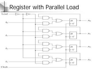
![44
Binary Counter with Parallel Load
n Counters employed in digital systems quite
often require a parallel load capability for
transferring an initial binary number into the
counter prior to count operation.
n The input load control when equal to 1
disables the count operation and causes a
transfer of data from the four data inputs
into the four flip-flops [Fig. 6-14]](https://image.slidesharecdn.com/sequentialcircuits-240209052844-4873578e/85/Sequential-circuits-Sequential-circuits1-44-320.jpg)


![47
Binary Counter with Parallel Load
n A counter with parallel load can be used to
generate any desire count sequence.
n [Fig.6-15] shows two ways in which a
counter with parallel load is used to generate
the BCD count.](https://image.slidesharecdn.com/sequentialcircuits-240209052844-4873578e/85/Sequential-circuits-Sequential-circuits1-47-320.jpg)


![52
Counter with Unused States
n The count has a repeated sequence of six
states.
n The simplified equations are:
n JA=B KA=B
n JB=C KB=1
n JC=B’ KC=1
n The logic diagram and state diagram is
shown in [Fig. 6-16]](https://image.slidesharecdn.com/sequentialcircuits-240209052844-4873578e/85/Sequential-circuits-Sequential-circuits1-52-320.jpg)

![54
Ring Counter
n A ring counter is a circular shift register with
only one flip-flop being set at any particular
time, all others are cleared.
n The single bit is shifted from one flip-flop to
the next to produce the sequence of timing
signals. [Fig. 6-17(a)] [Fig. 6-17(c)]
n The decoder shown in [Fig. 6-17(b)]
decodes the four states of the counter and
generates the required sequence of timing
signals](https://image.slidesharecdn.com/sequentialcircuits-240209052844-4873578e/85/Sequential-circuits-Sequential-circuits1-54-320.jpg)

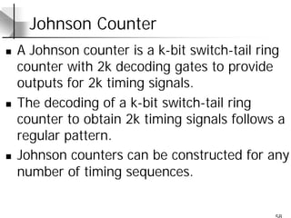
![56
Johnson Counter
n Generate the timing signals with a
combination of a shift register and a decoder,
which is called a Johnson counter.
n The number of states can be double if the
shift register is connect as a switch-tail ring
counter. [Fig. 6-18(a)]
n Starting from a cleared state, the switch-tail
ring counter goes through a sequence of
eight states, as shown in [Fig. 6-18(b)].](https://image.slidesharecdn.com/sequentialcircuits-240209052844-4873578e/85/Sequential-circuits-Sequential-circuits1-56-320.jpg)


![60
Shift Register
//Behavioral description of universal shift register Fig. 6-7 and Table 6-3
Module shftreg (s1,s0,Pin,lfin,rtin,A,CLK,Clr);
input s1,s0 //Select inputs
input lfin, rtin; //Serial inputs
input CLk, clr; //Clock and Clear
input [3:0] Pin; //Parallel input
output [3:0] A; //Register output
reg [3:0] A;
always @ (posedge CLK or negedge Clr)
if (~Clr) A = 4’ b0000’
else
case ({s1,s0}) //No change
2’ b00: A = A; //Shift right
2’ b01: A = {rtin,A[3:1]}; //Shift left
2’ b10: A = {A[2:0],lfin}; //Parallel load input
2’ b11: A =Pin;
endcase
endmodule](https://image.slidesharecdn.com/sequentialcircuits-240209052844-4873578e/85/Sequential-circuits-Sequential-circuits1-60-320.jpg)
![61
Shift Register
//Structural description of Universal shift register(see Fig.6-7)
module SHFTREG (I,select,lfin,rtin,A,CLK,Clr);
input [3:0] I; //Parallel input
input [1:0] select; //Mode select
input lfin,rtin,CLK,Clr; //Serial inputs,clock,clear
output [3:0] A; //Parallel output
//Instantiate the four stages
stage ST0 (A[0],A[1],lfin,I[0],A[0],select,CLK,Clr);
stage ST1 (A[1],A[2],A[0],I[1],A[1],select,CLK,Clr);
stage ST2 (A[2],A[3],A[1],I[2],A[2],select,CLK,Clr);
stage ST3 (A[3],rtin,A[2],I[3],A[3],select,CLK,Clr);
endmodule](https://image.slidesharecdn.com/sequentialcircuits-240209052844-4873578e/85/Sequential-circuits-Sequential-circuits1-61-320.jpg)
![62
Shift Register
//One stage of shift register
module stage(i0,i1,i2,i3,Q,select,CLK,Clr);
input i0,i1,i2,i3,CLK,Clr;
input [1:0] select;
output Q;
reg Q;
reg D;
//4x1 multiplexer
always @ (i0 or i1 or i2 or i3 or select)
case (select)
2'b00: D = i0;
2'b01: D = i1;
2'b10: D = i2;
2'b11: D = i3;
endcase
//D flip-flop
always @ (posedge CLK or negedge Clr)
if (~Clr) Q = 1'b0;
else Q = D;
endmodule](https://image.slidesharecdn.com/sequentialcircuits-240209052844-4873578e/85/Sequential-circuits-Sequential-circuits1-62-320.jpg)
![63
Synchronous Counter
//Binary counter with parallel load See Figure 6-14 and Table 6-6
module counter (Count,Load,IN,CLK,Clr,A,CO);
input Count,Load,CLK,Clr;
input [3:0] IN; //Data input
output CO; //Output carry
output [3:0] A; //Data output
reg [3:0] A;
assign CO = Count & ~Load & (A == 4'b1111);
always @ (posedge CLK or negedge Clr)
if (~Clr) A = 4'b0000;
else if (Load) A = IN;
else if (Count) A = A + 1'b1;
else A = A; // no change, default condition
endmodule](https://image.slidesharecdn.com/sequentialcircuits-240209052844-4873578e/85/Sequential-circuits-Sequential-circuits1-63-320.jpg)