Download to read offline


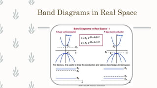
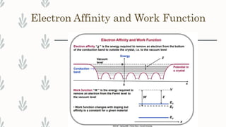

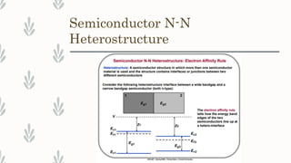
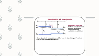
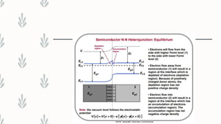
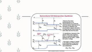
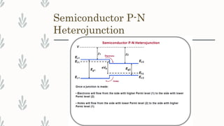
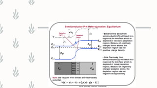
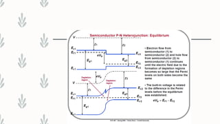

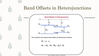
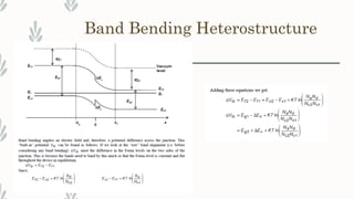
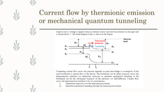
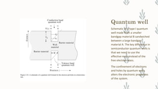
The document discusses semiconductor heterostructures, focusing on their band diagrams and types such as n-n and p-n junctions. It explains band offsets, band bending, and current flow mechanisms like thermionic emission and quantum tunneling. Additionally, it highlights the significance of effective mass in quantum wells formed from materials with different bandgaps, affecting the electronic properties of the system.


