1) The document discusses isolated and non-isolated bi-directional DC/DC converters for use in a Formula Hybrid electric vehicle.
2) It evaluates two isolated uni-directional converter topologies and discusses the working principles of three bi-directional converter topologies.
3) The goal is to determine the most efficient topology by conducting a comparative analysis to minimize losses.
![Isolated and Non-Isolated Bi-Directional
DC/DC Converters for Formula Hybrid
Racing ElectricVehicle
Marcus Howard, Ali Emadi and Alireza Khaligh
NSF – REU in Hybrid Electric and Plug-In Electric Vehicles
Energy Harvesting and Renewable Energies Laboratory (EHREL),
Electric Power and Power Electronics Center, Electrical and Computer Engineering Department,
Illinois Institute of Technology, 3301 S. Dearborn St., Chicago, IL, USA
E-mails: mhoward6@fvsu.edu, emadi@iit.edu, khaligh@ece.iit.edu; URL: www.ece.iit.edu/~khaligh/reu.php
Abstract- The Formula Hybrid International
Competition challenges students to design, build, and
race fuel efficient high-performance hybrid electric
vehicles. This event provides students and their
respective universities a chance to compete against each
other in a real world engineering environment. By
participating in this competition the Illinois Institute of
Technology (IIT) can teach students this advanced
technology for real world applications to this one of a
kind competition.
The WISER team at IIT has a cutting edge
student-designed hybrid electric vehicle for the 2011
competition. From this research, an evaluation of two
different isolated uni-directional DC/DC converter
topologies (a phase-shifted full-bridge ZVS PWM
converter, and a duty-cycle shifted half-bridge ZVS
PWM converter) will be examined. Also, the working
principles of three different bi-directional DC/DC
converter topologies (ZVS dual half-bridge converter,
conventional PWM converter, and synchronous
rectification PWM converter) are discussed.
I. INTRODUCTION
In May 2011, the IIT WISER team will compete
against several universities in an international
competition. The SAE International Formula Hybrid
competition challenges undergraduates and graduates
to design, build, and race high-performance hybrid
vehicles. The goal is better overall efficiency in
comparison to the standard ICE vehicles. For the
accumulator system, the WISER team will be using
lithium polymer batteries that are typically used in
RC aircraft. The configuration will consist of 30
individual cells in series and 8 strings in parallel
giving a nominal system voltage of 110 V and a
capacity of 48 Ahr. The vehicle topology will be a
series hybrid as seen in Figure 1. The powertrain
configuration will be four independent electric drive
utilizing four outboard hub mounted motors. Each
motor will drive the wheels through a 3.5:1 elliptical
gear train that is contained inside the vehicles
upright. A permanent magnet DC motor will be
coupled with an internal combustion engine to form a
genset [1, 2]. Lithium Polymer battery packs have
the best energy density in comparison to lead
acid/NiMH/Li-Ion. The approximate value of the
horsepower outputted by the motors is 120 hp. The
gen set will output at least 1.6 kW.
This study will introduce bi-directional DC/DC
converters that will enable the interactions of the high
voltage battery pack and the genset. Also, isolated
buck converters will enable operation of the electric
clutch, motor controllers, microcontrollers, lights,
relay coils, back-up battery pack, and the DAQ. The
objective is to determine which inverter minimizes
losses and is the most efficient. In order to achieve
the best performance, a comparative analysis will be
conducted to determine which topology is the most
efficient with accruing minimal losses.
II. WISER: SERIES HYBRID DESIGN
Figure 1. WISER Series Hybrid Powertrain Topology
The topology as seen in Figure 1 utilizes the
lithium-polymer battery pack for energy storage, the
electric motors for propulsion, and the combination
of the ICE and electric generator for power
generation [1, 2]. As shown in Figure 2, the bi-
directional DC/DC converters will provide electrical
power from the battery pack to the genset which will
be used by the electric traction motor or restore
energy back into the battery pack during regenerative
braking. Regenerative braking converts the formula
hybrid vehicle’s kinetic energy into electric energy
that can be stored in the lithium-polymer battery pack](https://image.slidesharecdn.com/a7dd541d-3d0e-4b53-a7d1-3cd16f31d3a9-150820215944-lva1-app6892/85/REU_report_paper-1-320.jpg)
![instead of being wasted as heat energy like
conventional brakes [7]. There are two modes of
operation in series hybrid electric vehicles, charge
depletion (CD) mode and charge sustaining (CS)
mode. In CD mode, the vehicle operation is
dependent upon energy from the battery pack. In CS
mode, the formula hybrid vehicle can remain within a
finite state of charge range for its accumulator [1, 2].
Charge-depleting mode is used at startup, and then
switches to charge-sustaining mode allowing the
vehicle to operate in all-electric mode. The series
topology simplifies the mechanical components that
have to be used in comparison to the parallel
topology [1, 2]. The series design allows for better
fuel economy and fuel efficiency because the electric
motor is more efficient than the ICE. A
microcontroller unit compares the power demanded
from the driver to the power outputted from the
battery pack to determine if extra power is required
from the generator [1, 2]. As shown in Figure 2, the
isolated buck converter will supply power to the
control systems as well as other electrical loads such
as the backup battery, lights, and the DAQ. The
DAQ, Data Acquisition system records and displays
real-time vehicle performance.
Figure 2. Formula Hybrid Vehicle Voltage System
III. SYSTEM DESCRIPTION
The WISER team’s formula hybrid electric
vehicle will utilize a permanent magnet DC
motor/generator to sustain energy to the internal
combustion engine. Figure 3a displays requirements
for operation of the permanent magnet DC motor that
will couple with the internal combustion engine.
P(rated) η(rated) I(rated) V(rated) ω(rated)
4 Hp 87% 75 A 48 V 694 rad/s
Figure 3a. Optimized values of the motor of the Genset
P(rated) η(rated) I(rated) V(rated) ω(rated)
23 Hp 91% 200 A 496 V 422 rad/s
Figure 3b. Optimized values for the wheel control motors
Figure 3b displays requirements for operation of the
permanent magnet DC motor that will control each
wheel. Bi-directional DC/DC converters will be
implemented to buck the voltage from the high
voltage battery pack to the genset in buck operation
and boost the voltage from the genset/motor to the
high voltage battery pack . The bi-directional
DC/DC converters in this paper will reflect the
operation of the motor used for the genset. The
system will convert the maximum voltage of 126 V
to the rated voltage of 48 V.
IV. OVERVIEW OF SWITCHING POWER
SUPPLIES
In switching power supplies, transformation of
DC voltage from one level to another is
accomplished by using DC/DC converter circuits.
These circuits employ transistors, MOSFETS,
IGBTs, etc. which operates comparable to an ideal
switch: either completely OFF or ON. Power
electronic devices aren’t required to operate in their
active region [18]. This mode of operation results in
lower power dissipations, increased switching speeds,
higher voltage and current ratings, and relatively
lower cost. By avoiding their operation in their
active region, significant reduction in power losses is
achieved resulting in higher energy efficiency, in the
range of 70 to 90% . Electrical isolation in feedback
loop is provided either through the isolation
transformer or optocoupler [21].
The average DC output voltage must be
controlled to equal a desired voltage level. The
average value Vo of the output voltage vo depends on
tON and tOFF [19]. In pulse width modulation (PWM)
the switch control signal that controls the ON or OFF
state is generated by comparing a signal level control
voltage vcontrol with a repetitive waveform. A control
voltage signal is obtained by amplifying the error or
difference between the actual output voltage and the
desired voltage [19]. When the amplified error
signal, which varies slowly with time relative to the
switching frequency is greater than the sawtooth
waveform, switch control signal becomes high,
causing switch to turn ON otherwise switch is OFF
[19].
V. THEORY OF OPERATION
A. UNIDIRECTIONAL DC/DC
CONVERTERS
Several topologies have been proposed for high
frequency isolated DC/DC conversion to reduce
component stresses and switching losses while
improving performance and sustaining high power
density. The following isolated DC/DC converters
researched are capable of transferring the 90-126 V
high voltage battery pack to 25V/4A for the small
electrical loads. As shown in Figure 5, the isolated
buck converter will buck the 126 V from the high
voltage battery pack to 25 V low voltage side. This
operation will enable control of the DAQ, lights,
relay coils, backup battery, and microcontrollers.
One of these proposed topologies is the phase-shifted
zero voltage switching (ZVS) full-bridge converter
[8]. Zero voltage switching conditions allow for
operation in the entire operating range and do not
generate parasitic oscillations that invoke voltage](https://image.slidesharecdn.com/a7dd541d-3d0e-4b53-a7d1-3cd16f31d3a9-150820215944-lva1-app6892/85/REU_report_paper-2-320.jpg)
![spikes. When the transistor current waveform and
voltage waveforms do not overlap, ZVS conditions
are fulfilled [21]. This condition makes the converter
devoid of the transistors switching power dissipation
within the whole operation range therefore it is
marked by high efficiency. The configuration of the
phase-shifted Full-Bridge ZVS PWM as shown in
Figure 4 allows all switches to operate at ZVS by
utilizing transformer leakage inductance and the
MOSFETs junction capacitance without having to
add an auxiliary switch. The complexity of the full-
bridge is cumbersome in comparison to the
conventional topologies due to its large switch count
and complicated control and driving of the circuit
[12].
Figure 4. Phase-shifted Full-Bridge ZVS PWM DC/DC Converter
Because of the simplicity of the half-bridge
converter topology it is very attractive for middle
power level applications. To achieve ZVS operation
for half-bridge DC/DC converters the asymmetric
control has been researched. Two drive signals are
complimentary generated turning on the high side
and low side switches. ZVS conditions are achieved
from the transformer primary current charging and
discharging the junction capacitance. The half-bridge
DC/DC converter has a DC gain ratio that is
nonlinear allowing operation beyond the optimum
operation point at high input voltage [8].
In this research, the duty-cycle shifted PWM
control displayed in Figure 5 will be analyzed for
determination if this topology is best suited for the
WISER’s Formula Hybrid Electric Vehicle. The
duty-cycle shifted PWM is applicable for a wide
input voltage range. Higher efficiency is expected
from the reduction of switching losses and
transformer leakage-inductance-related losses. This
control offers zero-voltage switching (ZVS)
operation for one of the two switches disallowing the
need to add extra components and without
asymmetric penalties of the asymmetric control [8].
This scheme shifts one of the two symmetric PWM
driving signals closer to the other, shortening the
resonant interval in the lagging switch achieving ZVS
operation. Energy trapped in the leakage inductance
is utilized for ZVS of the other switch. The duty-
cycle shifted PWM control scheme eliminates the
ringing result from the oscillation between the
transformer leakage inductance and the switches
junction capacitances during the OFF-time period [8].
Reverse recovery of the body diodes causes
significant harmonic distortion on the primary side
between the MOSFETs junction capacitance and the
transformer leakage inductance. Snubber circuits are
initialized to suppress the ringing. At, high current
and high switching frequencies losses dissipated in
the snubber become significantly large [20].
Figure 5. Duty-cycle shifted Half-Bridge PWM DC/DC Converter
Figure 6. Duty-cycle shifted HB PWM Control Waveforms
Figure 6 displays the key waveforms of the
researched duty-cycle shifted PWM half-bridge
converter. From symmetric PWM control, Vgs2 the
driving signal of S2 is shifts left bringing the Vgs2
rising edge closer to the falling edge of Vgs1 [8].
While S2 is turned off, current in the primary of the
transformer charges the junction capacitance of S2.
When the voltage across drain-to-source of S2
becomes zero, the current in the body diode of S2
conducts. S2 can be turned on during the body diode
conduction period, employing zero-voltage switching
operation. During this transition period, no ringing](https://image.slidesharecdn.com/a7dd541d-3d0e-4b53-a7d1-3cd16f31d3a9-150820215944-lva1-app6892/85/REU_report_paper-3-320.jpg)
![occurs [8]. For realization of the duty-cycle shifted
PWM control of the modulated carrier waveform is
vital. Using a repeated signal in the form of a
sawtooth waveform, -VC and VC are control voltages.
Gate drive signals for S1 and S2 are induced from
modulating –VC and VC. ZVS for S2 is achieved by
the falling edge of S1 being significantly close to the
rising edge of S2. The duty cycle of S1 is allocated
by shifting its rising edge left and right. The duty
cycle of S2 is allocated by shifting its falling edge
right and left. Because VC and –VC are
symmetrically centered about its zero axis, S1 and S2
retain the same duty cycle, as shown in the Figure 7
[8].
Figure 7. Duty-cycle shifted HB PWM Modulation Waveforms
In comparison to the conventional symmetric
PWM controller, the duty-cycle shifted PWM
controlled half-bridge dc/dc converter has identical
voltage-second values and magnetizing B-H of the
transformer and matching voltage and current
stresses in the primary side and secondary side [8].
Correlating to the design and characteristics of the
transformer for both systems are equivalent. From
the asymmetric PWM control there are asymmetric
penalties that allow the duty-cycle shifted PWM to
operate in a wide input voltage range [8]. Made
possible by the secondary inductor current reflecting
into the transformer primary side and discharging the
output capacitor of S2 creating a zero voltage
switching condition [8]. From analysis of the data
researched the duty-cycle shifted PWM ZVS half-
bridge DC/DC converter in comparison to the
conventional ZVS PWM half-bridge DC/DC
converter is more efficient. Even though the
conventional topology employs zero-voltage
switching methodology its switching characteristics
are not instantaneous like the duty-cycle shifted
PWM ZVS DC/DC converter.
B. BI-DIRECTIONAL DC/DC
CONVERTERS
Conventional bi-directional DC/DC converters
operate with their inductor current flowing in both
directions during each cycle. The drawback is the
inductor has a lot of ripple with very high peaks.
Additional filtering is needed to reduce the voltage
ripple. Soft switching using quasi-resonant or multi-
resonant techniques is another type of converter that
yields high peak voltage and/or current stresses [17].
This method could force the converter to operate with
variable switching frequency control which
complicates the design when factoring the magnetic
and filtering elements. An auxiliary circuit could be
employed to assist switches to operate with soft
switching as done in zero voltage transition (ZVT)
converters. Using this method is costly and complex.
There have been several techniques proposed for high
frequency DC/DC conversion to reduce component
stresses and switching losses while improving
performance and sustaining high power density [12].
A ZVS dual half-bridge bi-directional DC/DC
converter has been researched to accomplish the task
of converting the 126V from the high voltage battery
pack to 48 V needed for the genset. When compared
to the full-bridge bi-directional DC/DC converter,
this topology has half the component count with the
same power rating and no total –device-rating penalty
[5, 6]. This system is easier to control and has an
efficient power conversion. The ZVS dual half-
bridge DC/DC converter researched increases the
order of the system.
Figure 8. ZVS Bi-directional Half-Bridge DC/DC Converter
Figure 8 displays the ZVS dual half-bridge
DC/DC converter. Zero voltage switching is
generated from the two half-bridges operating with a
phase shift. Before the switching devices conduct
there is a resonant discharge of the lossless snubber
capacitances of the switching devices and each
device’s antiparallel diode [5, 6]. Each switch
instantaneously turns ON or OFF. Transformer
leakage inductance is utilized as an energy transfer
element between the high voltage side and low
voltage side [5,6]. There are four modes of operation
in one switching cycle. In each mode the transformer](https://image.slidesharecdn.com/a7dd541d-3d0e-4b53-a7d1-3cd16f31d3a9-150820215944-lva1-app6892/85/REU_report_paper-4-320.jpg)
![current ir can be calculated. From the symmetric
property of dual active half-bridges, boost mode and
buck mode operation principles are identical except
for the polarity of the phase shift angle [5, 6]. An
averaged model can be developed for both modes.
Output voltage is regulated by controlling the
switching frequency and phase shift. A controller has
to be implemented to stabilize the system and reduce
the effect of exogenous disturbances in the system [5,
6].
Analysis of the data researched leads to the
conclusion this topology is a great candidate to be
employed in the WISER’s Formula Hybrid Vehicle.
Although a better controller can be derived for this
system in its current state has an overshoot of output
voltage of less than 0.2% [5, 6]. When the input
voltage is changed 1V the reference remains at the
desired output. The systems response to a load step
change was exceptional, overshoots are negligible [5,
6].
For this research, a non-isolated bi-directional
DC/DC converter is proposed to control the flow of
energy between the high voltage battery pack and
permanent magnet DC motor. Conventional PWM
control, as shown in Figure 9a, and synchronous
rectification PWM control, as shown in Figure 9b,
are explored to determine efficiency gained from
implementing synchronous rectification. The
Formula Hybrid Electric Vehicle will employ a
DC/DC converter that bucks the 90- 126 V from the
high voltage battery pack to 48 V utilized by the
permanent magnet DC motor to initialize start-up and
maintain idle speed, and boosts the 48 V from the
motor to 126 V for the high voltage battery pack.
There are two modes of operation in all
converters, continuous conduction mode (CCM) and
discontinuous conduction mode (DCM). In
discontinuous conduction mode, inductor current
reaches zero in one switching cycle producing a non-
linear relationship with the input voltage. In
continuous conduction mode, inductor current never
reaches zero enabling a linear relationship with the
input voltage [18]. My analysis and simulation
focuses on utilizing CCM. This mode offers high
efficiency and optimal utilization of passive
components and semiconductor switches.
Figure 9a. Non-Isolated Bidirectional PWM DC/DC Converter
Figure 9b. Non-Isolated Bidirectional Synchronous Rectification
PWM DC/DC Converter
In buck mode operation for conventional PWM,
as depicted in Figure 9a, when S1 is ON and S2 is
OFF, enacting the antiparallel body diode of the
MOSFET which is in reverse bias, energy is provided
from the input to the inductor and load [21]. During
the OFF state transition, when both S1 and S2 are
OFF, the antiparallel body diode of S2 is forward
biased while S1 is in reverse bias allowing the
inductor current to transfer stored energy into to the
load [21].
The diode forward voltage drop is appreciable,
reducing the converter efficiency during the second
cycle [22]. In order to avoid shunt supply currents,
non-overlap logic must be implemented during
synchronous rectification. During synchronous
rectification PWM switching control, when S2 is ON
and S1 is OFF, current drifts upward out of the drain
of S2 achieving higher efficiency [9].
In continuous conduction mode, the duty cycle
of the S1 for a given input voltage varies linearly with
the output voltage. This is equivalent to transformer
operation where the turns ratio can be continuously
controlled electronically from a range of 0 to 1 by
controlling the duty cycle of the switch [18]. To
eliminate undesired current harmonics large
capacitors are employed as filters for the input
voltage and output voltage. During each switching
cycle the change in the net capacitor charge is zero
[20]. The output capacitor becomes a temporary
storage unit for surplus loads and inductor currents.
Faraday’s law states the inductor volt-second product
over a period of steady-state operation is zero [9].
When considering design parameters for the
buck converter, high switching frequencies are
desired to reduce the size of the capacitor and
inductor [20]. There is a trade-off when increasing
the switching frequency, power loss in the switches is
increased. A larger heat sink is required from the
increased power loss of the switches and the
converter’s efficiency decreases [21]. Switching
frequencies typically should be greater than 20 kHz
so the component vibrations are inaudible. The
inductor value should at least 25% larger than the
minimum inductance obtained from calculations, for
optimization [22]. The inductor core cannot saturate
for peak inductor current and the inductor wire have
to be rated at the rms current value [18]. The switch,](https://image.slidesharecdn.com/a7dd541d-3d0e-4b53-a7d1-3cd16f31d3a9-150820215944-lva1-app6892/85/REU_report_paper-5-320.jpg)
![either a metal-oxide-semiconductor field-effect
transistor (MOSFET) or an insulated-gate bipolar
transistor IGBT), and diode have to withstand the
maximum voltage stress in the OFF state and
maximum current in the ON state. Steady state
analysis is assumed when configuring design
parameters and the components are ideal [18]. The
duty cycle for continuous current is calculated from
the ratio of output voltage to source voltage: ܦ =
(
௦
). The minimum inductor size is calculated using
the equation: ݊݅݉ܮ =
(ଵି)ோ
ଶ
[21, 22]. The average
inductor current and the change in current are figured
using the equations: ݈ܫ = ቀ
ோ
ቁ and ∆݈݅ = (
௦ି
) ×
.ܶܦ The ripple requirement in inductor current
dictates the value of the inductor [9]. The change in
current generally lies within 10-20% of the maximum
value of the output current [18]. The minimum and
maximum inductor currents are calculated using the
equations: ݔܽ݉ܫ = ݈ܫ + (
∆
ଶ
) and ݊݅݉ܫ =
݈ܫ − ቀ
௱
ଶ
ቁ . To compute the inductor rms current for
the offset triangular wave the following equation is
used: ,݈ܫ ݏ݉ݎ = ට((݈ܫଶ) + ((
∆
ଶ
)/(√3))ଶ . The
capacitor is selected from the equation: ܥ =
(
ଵି
଼ቀ
೩ೇ
ೇ
ቁమ
) [21, 22].
In boost mode the output voltage is greater than
the input voltage, as shown in Figure 9a. When the
conventional PWM switching control is
implemented, S2 is ON and the current in the inductor
rises linearly while the capacitor partially discharges
supplying current to the load [21]. Amid the second
interval, S2 is OFF and the body diode of S1 is
forward biased allowing the inductor to provide
current to the load and recharge the capacitor. To
achieve the steady state output voltage equation the
inductor-volt balance principle is used [22]. Due to
the output voltage being greater than the input
voltage, the inductor current which is the input
current is larger than the output current. At high duty
cycles the efficiency of a boost converter degrades
exponentially [20].
To configure design parameters for Boost mode
operation for the non-isolated bidirectional DC/DC
converter the following criteria are analyzed. The
analysis assumes that steady state conditions exist
and the components are ideal [18]. Determine the
duty ratio of the converter using the equation:
ܦ = 1 − (
௦
). For continuous current to be
determined the minimum inductance must be
calculated: ݊݅݉ܮ =
൫(ଵି)మ൯ோ
ଶ
. The capacitor
value is determined using the equation: ܥ >
ோቀ
∆ೇ
ೇ
ቁ
. The average current in the inductor is
determined from the equation: ݈ܫ =
௦
(ଵି)మோ
. The
maximum and minimum inductor current values also
have to be considered. There are computed using the
following equations: ݔܽ݉ܫ = ݈ܫ + (
௦்
ଶ
) and
݊݅݉ܫ = ݈ܫ − (
௦்
ଶ
) [21, 22].
VI. CONTROL STRATEGY
Input voltage and the output load can fluctuate
but the average DC output voltage and current must
to be controlled to equal the desired levels of the
WISER team’s Formula Hybrid Electric Vehicle
specifications. Controlling the switch ON and OFF
durations determines the average output voltage.
Pulse-Width Modulation switching, commonly
referred to as the switch duty ratio D, is the ratio of
the ON-duration to the switching time period [18-22].
The control voltage signal is generated from
obtaining the amplified error, or difference between a
desired value and the actual voltage controlling the
ON and OFF state of the switch. Similar to the
waveforms depicted in Figure 7. When the amplified
error signal becomes greater than the sawtooth
waveform the switch control signal becomes high
enabling switch operation [19].
Design analysis for the feedback loop of the
bidirectional DC/DC converter boost mode operation
led to the construction of a power controller, as
shown in figure 10a and 10b. Since the output for
boost mode is a voltage source the current into the
system needs to be controlled [19]. Both of these
methods use current as the reference in regards to the
Proportional-Integral-Derivative controller. The
cascaded design assists in the elimination of
oscillations in the output signals. The Proportional-
Integral-Derivative controller (PID) takes the
difference between the reference value and the actual
value, the tracking error, and determines the
derivative and integral of the signal [23]. The
proportional controller will effectively reduce the rise
time. However, it cannot discard the steady-state
error. The integral controller can eliminate the
steady-state error. The integral controller has the
ability to worsen the transient response. The
derivative controller stabilizes the system [23].
Accomplishes this task by reducing the overshoot and
enhance the transient response.
The power controllers in Figure 10a and Figure 10b
allow the reference power of the genset to be applied
to the high voltage battery pack. The high voltage
battery pack’s charging power can be maintained
from the desired reference power. This reference
power is determined from the state of charge from the
battery [19]. The high voltage battery pack will
accommodate the power received during regenerative
braking.](https://image.slidesharecdn.com/a7dd541d-3d0e-4b53-a7d1-3cd16f31d3a9-150820215944-lva1-app6892/85/REU_report_paper-6-320.jpg)
![Figure 10a. Bidirectional DC/DC Converter Boost Mode Power
Controller
Figure 10b. Bidirectional DC/DC Converter Boost Mode Power
Controller
Design analysis of the feedback loop for buck
mode operation in the bidirectional DC/DC converter
led to the implementation of a voltage controller, as
in figure 11. The output for buck mode is basically
to a current source load with nominal resistance. The
voltage to the load needs to be under control. In the
voltage controller, the Permanent Magnet DC
motor’s voltage is the reference voltage for the PID
controller. The duty cycle is determined from the
output of the PID and compared with the sawtooth
signal [19]. The resulting signal is applied to S1/S2.
Figure 11. Bidirectional DC/DC Convert Buck Mode Voltage
Controller
VII. SOFTWARE
MATLAB version 7.6.0.324 (R2008a) was the
software used to conduct simulations of the proposed
circuits. With the use of the SimPower Systems
library, unidirectional and bidirectional DC/DC
converters were designed and simulated.
VIII. SIMULATION RESULTS
The schematic diagram of Figure 9a and 9b were
constructed in Simulink. The circuits were modeled
first at ideal source and load conditions. Operating at
the input and output specifications declared by the
WISER team, simulation results yielded a DC/DC
conversion of 110 V to 48 V in buck mode and 48 V
to 128 V in boost mode. The results from the buck
mode operation are closed loop values, whereas boost
mode operation results are open loop values. The
Simulink library did not have a permanent magnet
DC motor in SimPower Systems but has a separately
excited DC motor on file. The parameters of the
separately excited DC motor were configured to
behavior responses similar to the permanent DC
motor. The Simulink library did not have a lithium-
polymer battery. A lithium-ion battery modeled to
have similar characteristics as the lithium-polymer
battery is used as the power source. The switching
frequency of the system is 75 khz. S1 and S2 are
modeled after off the shelf components. The value of
the inductor is 2.5 mH. The value of the capacitors is
3333µF.
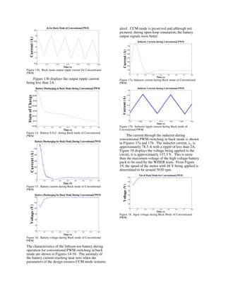
Figure 12a. Buck mode output voltage for Conventional PWM
Figure 12b. Buck mode output ripple voltage for Conventional
PWM
Conventional PWM switching in buck mode has
an output voltage that is approximately 48.5 V as
shown in Figure 12. The output ripple voltage is less
than 10mV as depicted in Figure 12b.
Figure 13a. Buck mode output current for Conventional PWM
Figure 13a shows that the output current during
conventional PWM switching in buck mode is
approximately 78 A.
0 0.1 0.2 0.3 0.4 0.5 0.6 0.7 0.8
0
10
20
30
40
50
60
Time (s)
Voltage(V)
Vo for Buck Mode of Conventional PWM
0.72 0.725 0.73 0.735 0.74 0.745 0.75 0.755 0.76
48.4
48.45
48.5
48.55
48.6
48.65
48.7
48.75
48.8
Time (s)
Voltage(V)
Vo for Buck Mode of Conventional PWM
0 0.1 0.2 0.3 0.4 0.5 0.6 0.7 0.8
0
100
200
300
400
500
600
700
Time (s)
Current(A)
Io for Buck Mode of Conventional PWM](https://image.slidesharecdn.com/a7dd541d-3d0e-4b53-a7d1-3cd16f31d3a9-150820215944-lva1-app6892/85/REU_report_paper-7-320.jpg)


![the duty-cycle shifted PWM is instantaneous, unlike
other topologies. From the asymmetric PWM control
there are asymmetric penalties that allow the duty-
cycle shifted PWM to operate in a wide input voltage
range. The duty-cycle shifted PWM ZVS half-bridge
DC/DC converter in comparison to the conventional
ZVS PWM half-bridge DC/DC converter is more
efficient. An inference can be drawn that the duty-
cycle shifted PWM ZVS half-bridge DC/DC
converter is comparably efficient to the phase-shifted
full-bridge ZVS PWM DC/DC converter since there
is a reduction is switch count. Since, the duty-cycle
shifted PWM ZVS half-bridge DC/DC converter can
be constructed and operated at cheaper price
producing the same results. The duty-cycle shifted
PWM ZVS half-bridge DC/DC converter is my
selection for usage by the WISER team for their
Formula Hybrid Electric Vehicle to isolate the low
electrical loads from the high voltage battery pack.
XI. ETHICS IN ENGINEERING
Technology has double implications: it creates
benefits along with fostering moral dilemmas.
Researchers should avoid allowing technological
risks to surpass technological benefits. Moral values
are ingrained in engineering projects as standards of
eminence. Morally good judgment and technical
skill should dictate the solution when faced with an
ethical dilemma. Researchers encounter both
technical and moral problems involving the quality of
work by coworkers, materials available to them, and
the pressure imposed by duration to complete project.
Researchers should form consistent and
comprehensive viewpoints based on the data. One
should be willing to apply moral reasonableness.
There has to be a respect for ethnic and religious
differences. There should be a rational dialogue
when resolving ethical dilemmas.
ACKNOWLEDGEMENT
This work has been supported by the U.S.
National Science Foundation under Grant number
0852013, which is greatly acknowledged.
REFERENCS
[1] Jonathan Sibley, S. G. Wirasingha, and Ali Emadi,
“Formula Hybrid Racing at Illinois Institute of Technology:
Academic Year 2007/2008,” in Proc. IEEE Vehicle Power
and Propulsion Conference, Sept. 2008, Harbin, China.
[2] Garrett T. Nielson, Jonathan Sibley, Sanjaka G.
Wirasingha, Antonis I. Antoniou, and Ali Emadi, “Formula
Hybrid Racing at Illinois Institute of Technology:
Academic Year 2008/2009,” in Proc. IEEE Vehicle Power
and Propulsion Conference, Sept. 2009, Dearborn, MI.
[3] Riku Pöllänen, Antti Tarkiainen, and Olli Pyrhönen,
“Simulation of current-mode controlled DC-DC boost
converter in chaotic regime evaluating different simulation
methods,” Electrical Engineering (Archiv fur
Elektrotechnik), vol. 88, no. 1, July 2004, pp. 35-44.
[4] Hui Li, F. Z. Peng, and J. S. Lawler, “ZVS Medium-
Power DC-DC Converter with Minimum Number of
Devices,” IEEE Transactions of Industry Applications, vol.
39, no. 2, April 2003, pp. 525-535.
[5] Hui Lu, and F. Z. Peng, “Modeling of a New ZVS Bi-
Directional DC-DC Converter,” IEEE Trans. On Aerospace
and Electronic Systems,” vol. 40, no. 1, pp. 272-283, Jan.
2004.
[6] Y. Lee, A. Khaligh, and A. Emadi, “Advanced
Integrated Bidirectional AC/DC and DC/DC Converter for
Plug-In Hybrid Electric Vehicles,” IEEE Trans. Veh.
Technol., vol. 58, no. 8, pp. 3970-3980, Oct. 2009.
[7] A. Emadi, S. Williamson, and A. Khaligh, “Power
Electronics Intensive Solutions for Advanced Electric,
Hybrid electric, and Fuel Cell Vehicular Power Systems,”
IEEE Trans. Power Electronics, vol. 21, no. 3, pp. 567-
577, May 2006.
[8] R. Madhusudhanan, and S. Rama Reddy. “Digital
Simulation of ZVS DC to DC Converter Using Simulink.”
European Journal of Scientific Research, vol. 23, no. 2,
2008, pp.317-329.
[9] Saurabh Kasat, Analysis, Design and Modeling of DC-
DC Converter Using Simulink, M.S. Thesis, Oklahoma
State University, December 2004.
[10] Sangtek Han, and D. Divan, “Bi-directional DC/DC
converters for plug-in hybrid electric vehicles (PHEV)
applications,” in Proc. IEEE 23rd
Applied Power
Electronics Conference, Austin, TX, Feb. 2008.
[11] S. Jalbrzykowski, and T. Citko, “A bi-directional
DC/DC converter for renewable energy systems,” Bulletin
of the Polish Academy of Sciences, Technical Sciences, vol.
57, no. 4, 2009, pp. 363-368.
[12] F. Krismer, J. Biela, and J. W. Kolar, “A Comparative
Evaluation of Isolated Bi-directional DC/DC Converters
with Wide Input and Output Voltage Range,” in Proc.
IEEE 40th
Industry Applications Conference, Hong Kong,
China, Oct. 2005.
[13] . Jalbrzykowski, and T. Citko, “Current-Fed Resonant
Full-Bridge Boost DC/AC/DC Converter,” IEEE
Transactions on Industrial Electronics,” vol. 55, no. 3,
March 2008, pp. 1198-1205.
[14] I.Khan, “DC-to-DC Converters for Electric and
Hybrid Vehicles,” in Proc. IEEE Power Electronics and
Transportation Conference, Dearborn, MI, Oct. 1994.
[15] S. Kim, W. Jang, J. Song, O. Kang, and H. Kim, “A
Novel Isolated Buck-Boost Converter,” in Proc. IEEE 31st
Telecommunications Energy Conference, Incheon, South
Korea, Oct. 2009.
[16] B.Laan, P. Das, S. A. Mosavi, and G. Moschopoulos,
“A Novel Bidirectional PWM DC-DC Converter,” in Proc.
IEEE Electrical and Computer Engineering Conference,
Niagara Falls, ON, May 2008.
[17] M. Gang, L. Yuanyuan, and Q. Wenlong, “A Novel
Soft Switching Bidirectional DC/DC Converter and its
Output Characteristics,” in Proc. IEEE 5th
International
Power Electronics and Motion Control Conference,
Shanghai, China, Feb. 2009.
[18] Ned Mohan, Tore Undeland, and William Robbins,
“Power Electronics: Converters, Applications and Design,”
New York, NY: John Wiley & Sons, 1989.](https://image.slidesharecdn.com/a7dd541d-3d0e-4b53-a7d1-3cd16f31d3a9-150820215944-lva1-app6892/85/REU_report_paper-14-320.jpg)
![[19] Abraham Pressman, Keith Billings, and Taylor Morey,
“Switching Power Supply Design, 3rd
ed.,” New York, NY:
McGraw-Hill, 2009.
[20] Barry Williams, “Principles and Elements of Power
Electronics: Devices, Drivers, Applications and Passive
Components,” Glasgow: Barry Williams, April 2006.
[21] Robert Erickson and Dragan Maksimovic,
“Fundamentals of Power Electronics, 2nd
ed.,” New York,
NY: Springer, January 2001.
[22] Daniel Hart, “Introduction to Power Electronics,”
Upper Saddle River, NJ: Prentice Hall, 1997.
[23] Aiden O’Dywer, “Handbook of PI and PID Controller
Tuning Rules, 3rd
ed.,” Covent Grove, London: Imperial
College Press, 2009.](https://image.slidesharecdn.com/a7dd541d-3d0e-4b53-a7d1-3cd16f31d3a9-150820215944-lva1-app6892/85/REU_report_paper-15-320.jpg)


![6.[36 45]seven level modified cascaded inverter for induction motor drive app...](https://cdn.slidesharecdn.com/ss_thumbnails/6-36-45sevenlevelmodifiedcascadedinverterforinductionmotordriveapplications-111118181646-phpapp02-thumbnail.jpg?width=640&height=640&fit=bounds)


![2100069076 [Autosaved].pptx jnunuuhhihihhi](https://cdn.slidesharecdn.com/ss_thumbnails/2100069076autosaved-251230044957-c15eebae-thumbnail.jpg?width=640&height=640&fit=bounds)


