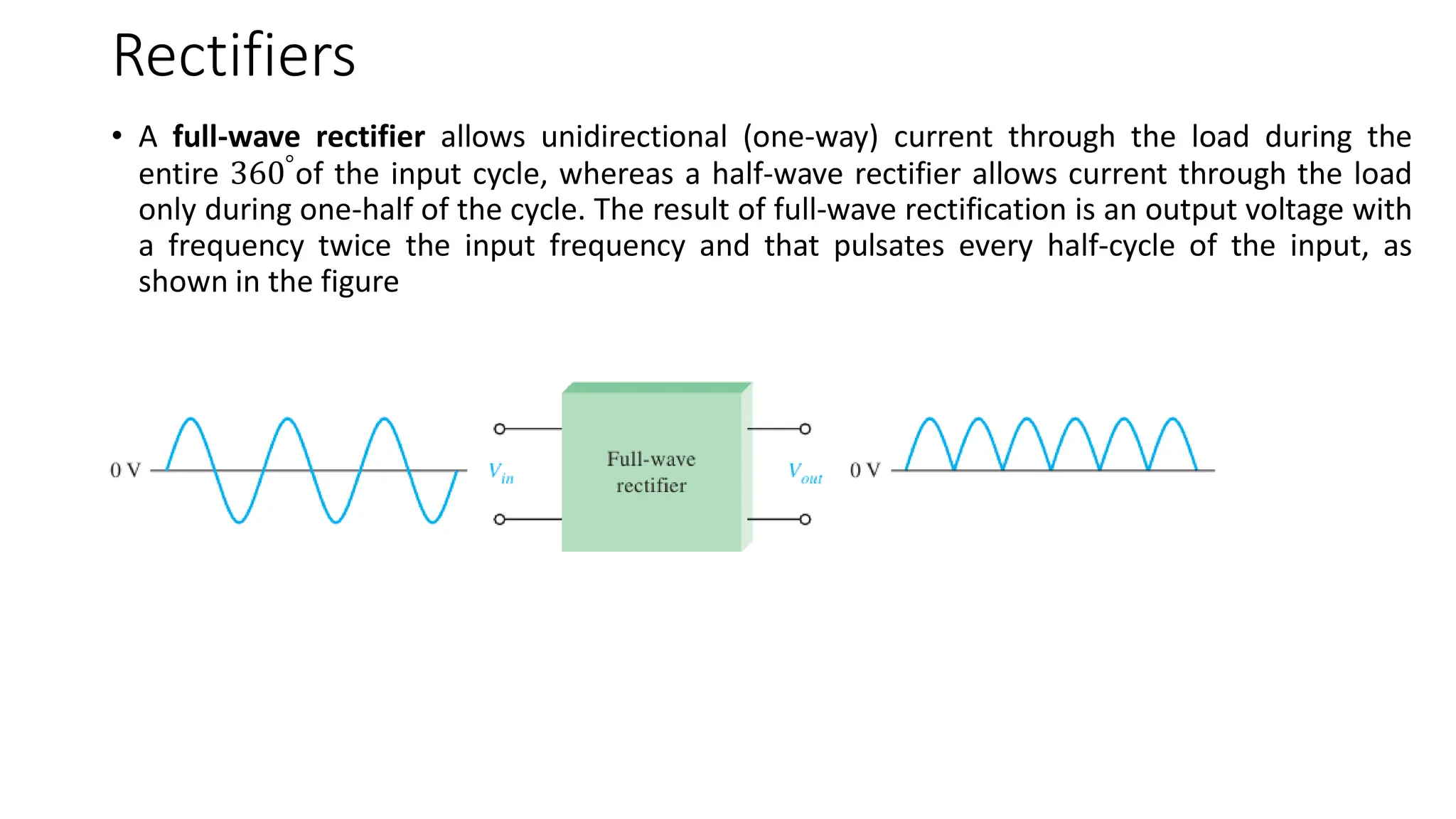
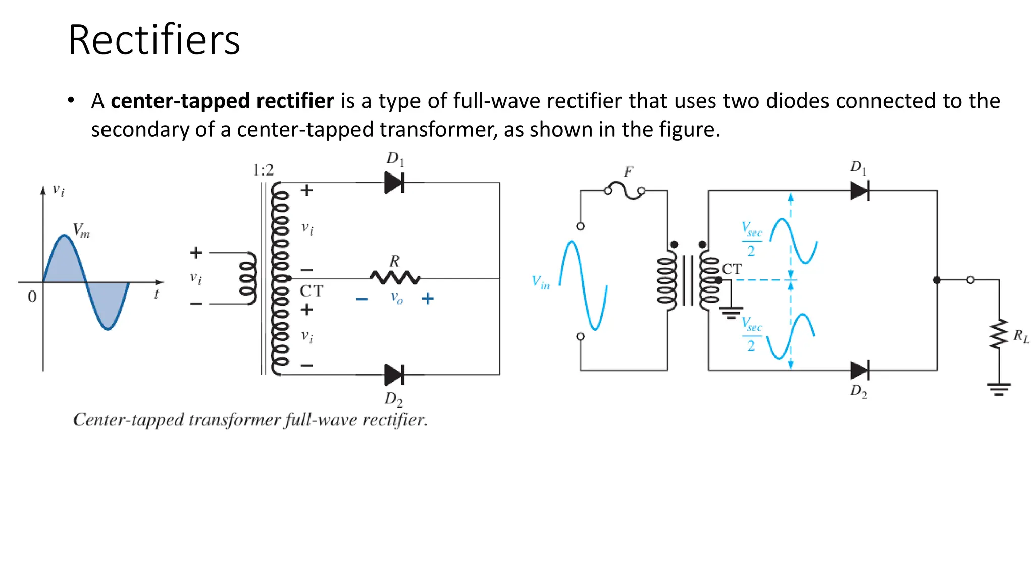
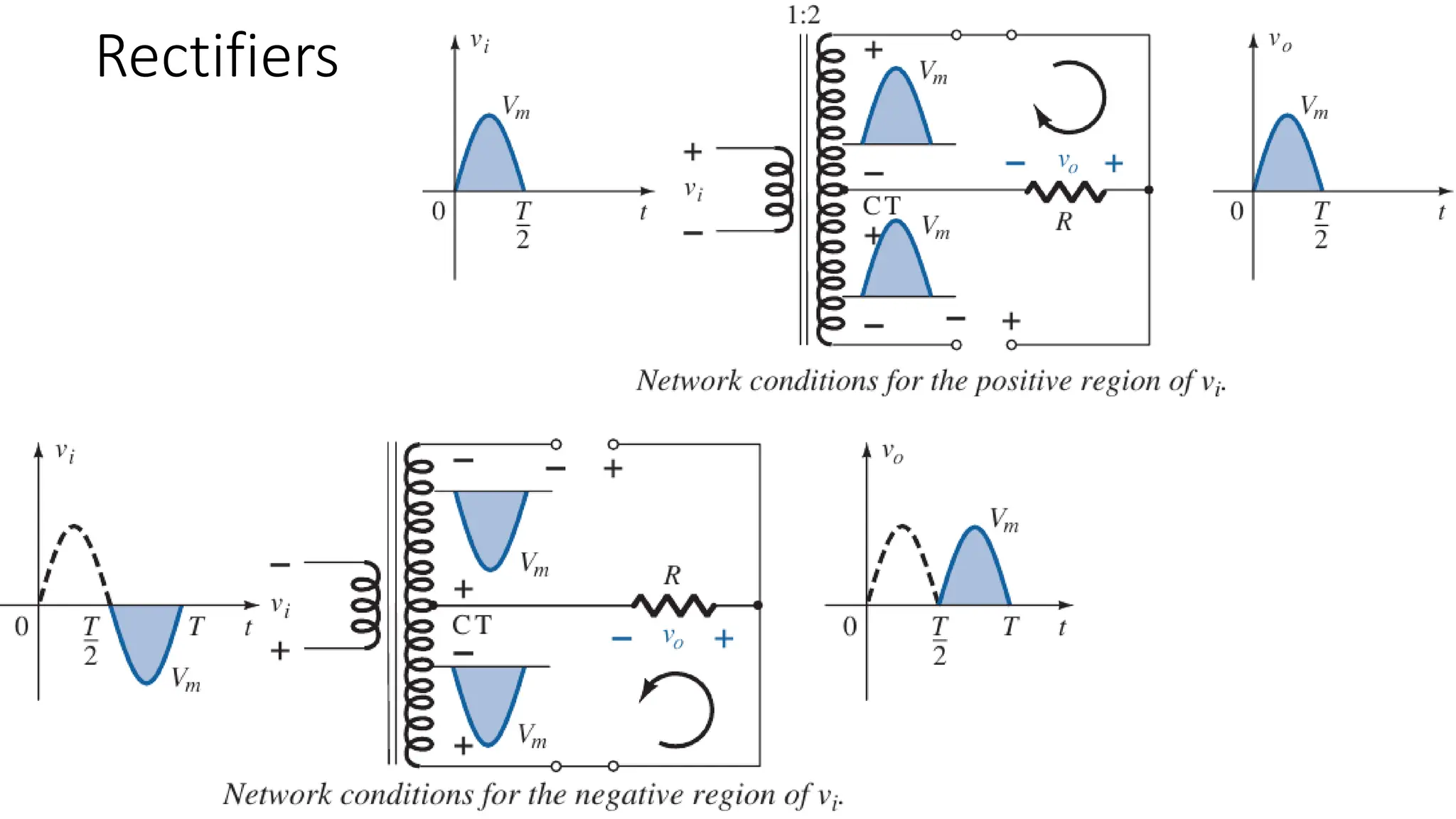
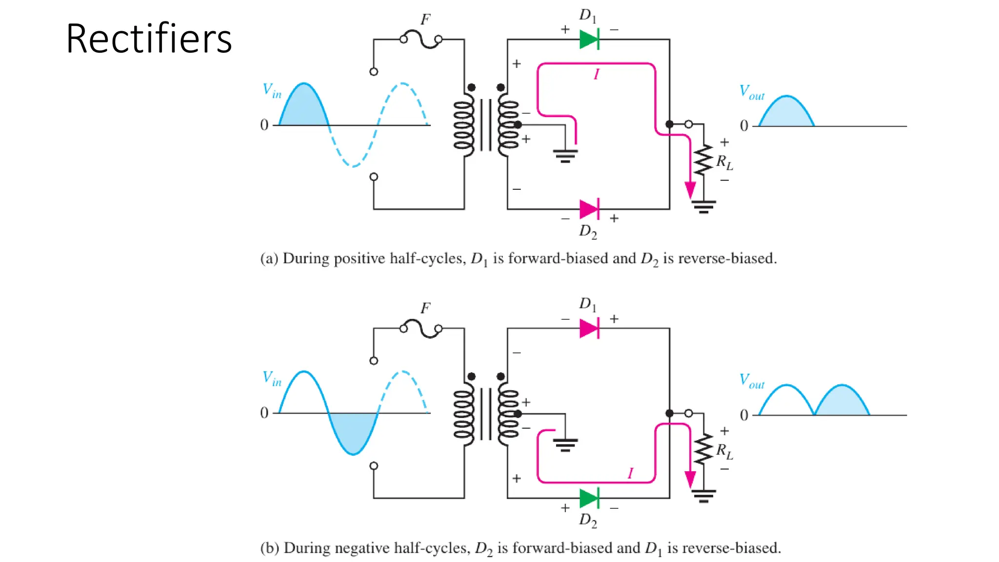
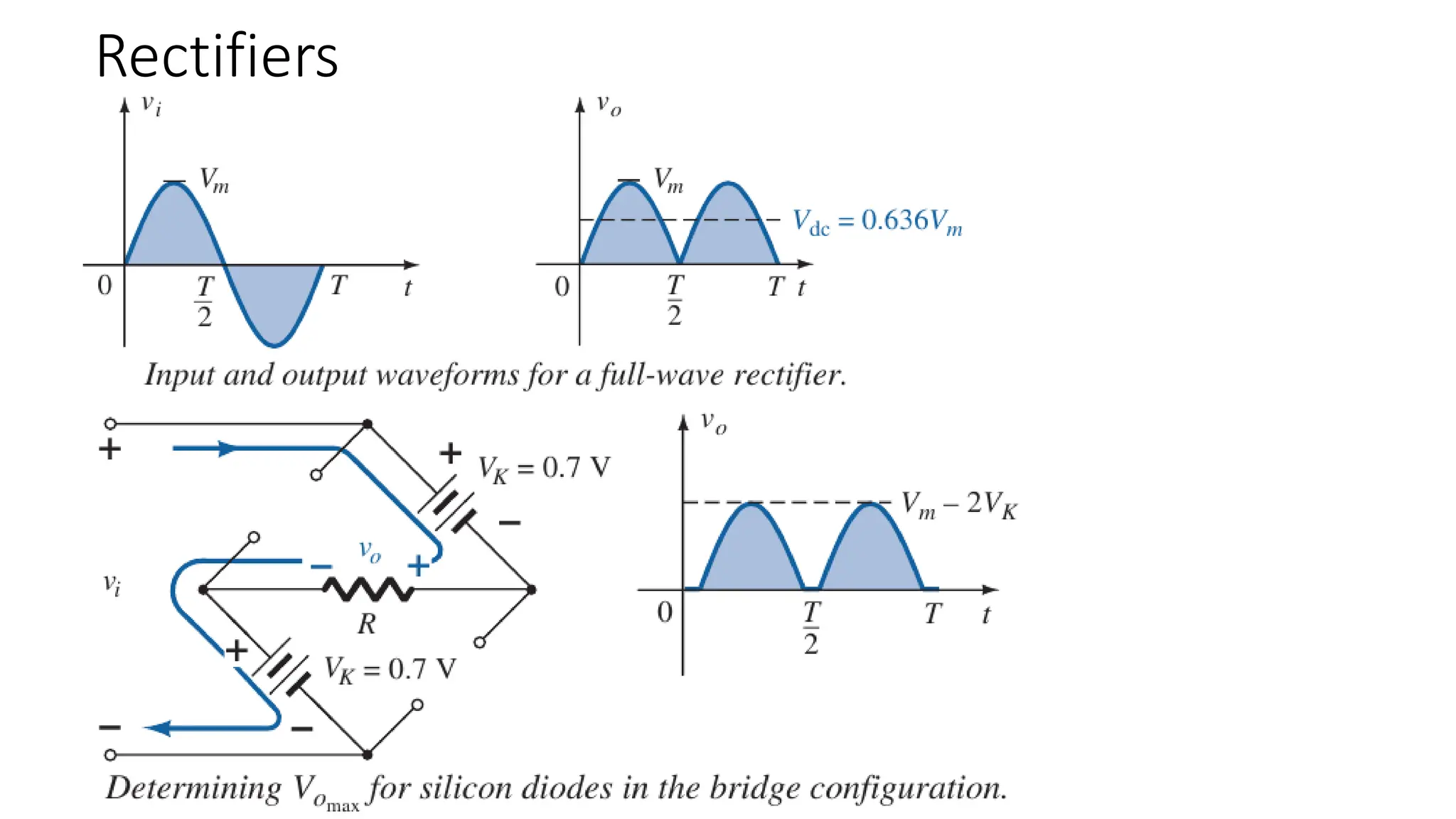
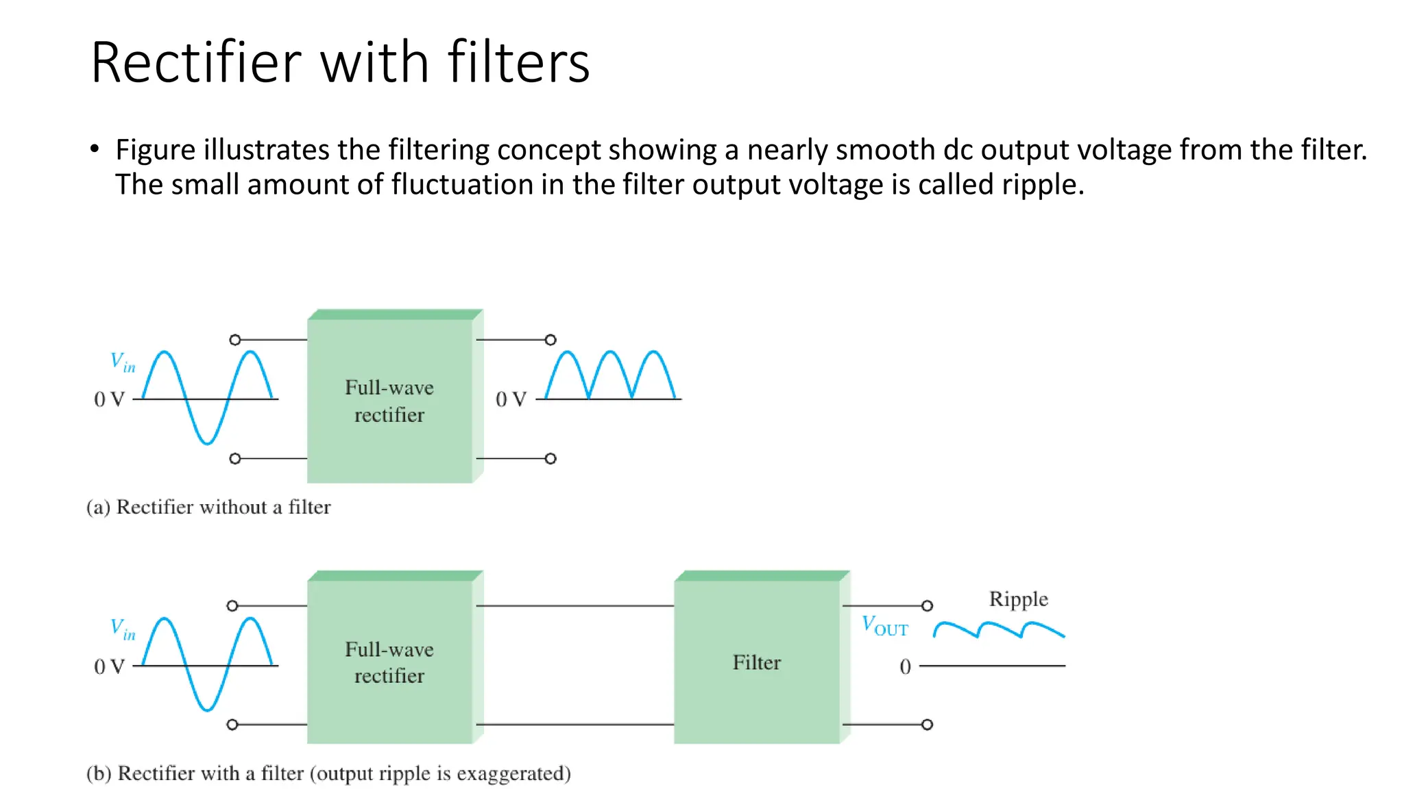
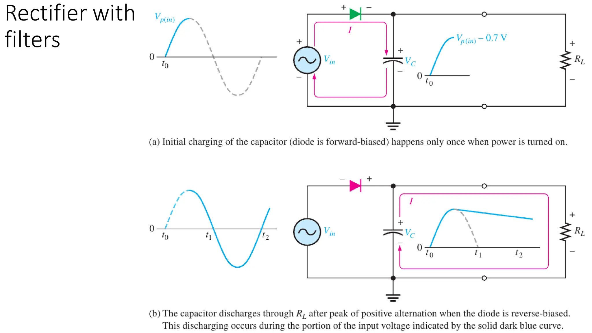
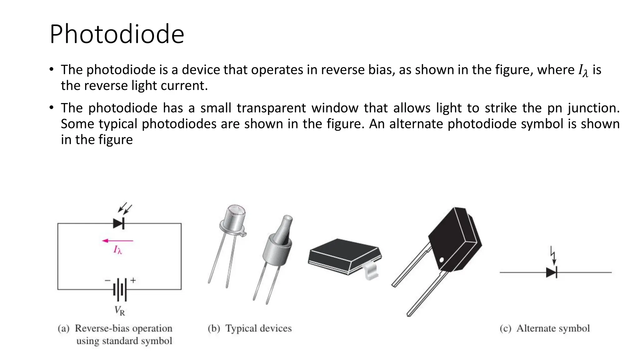
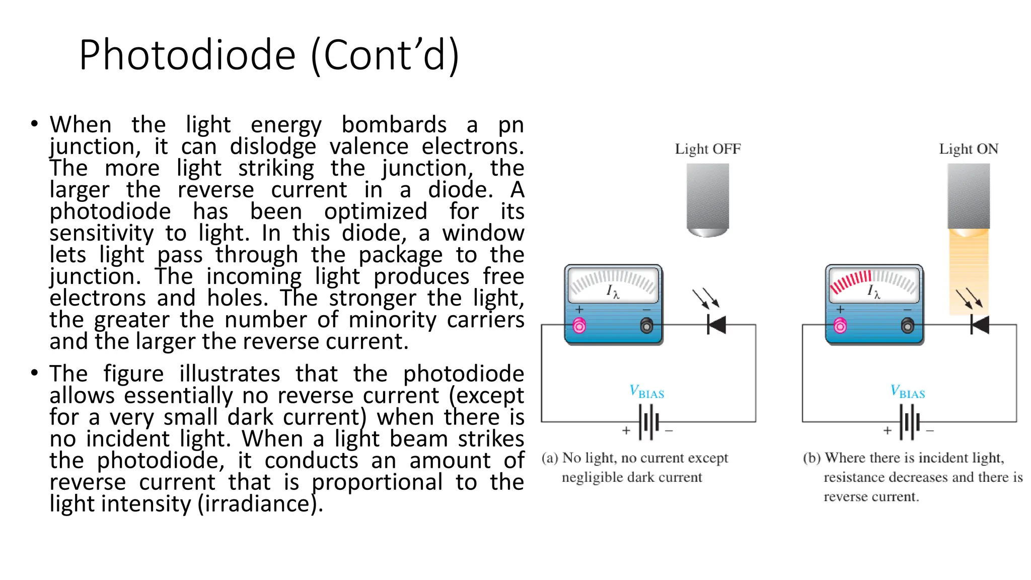
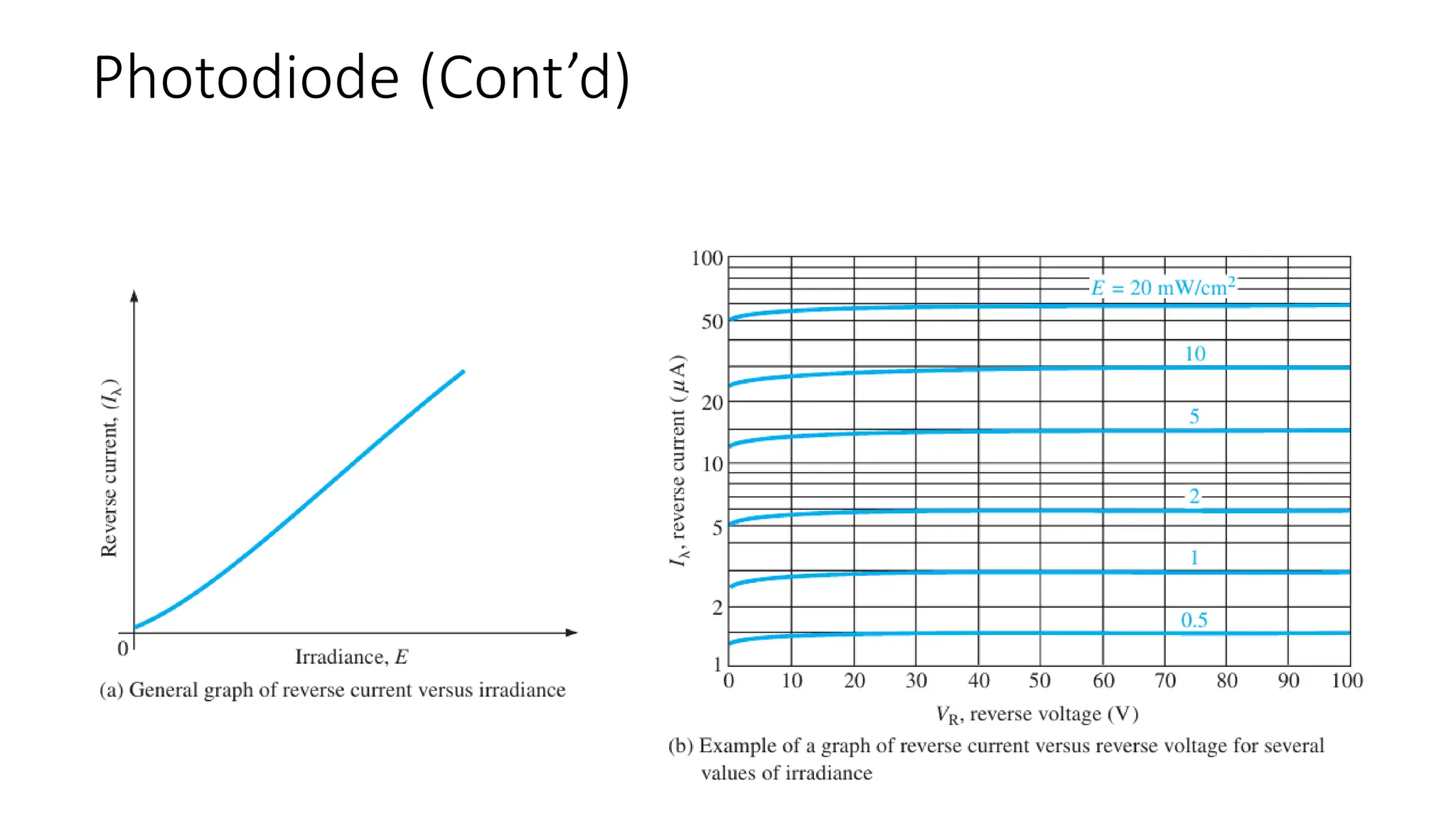
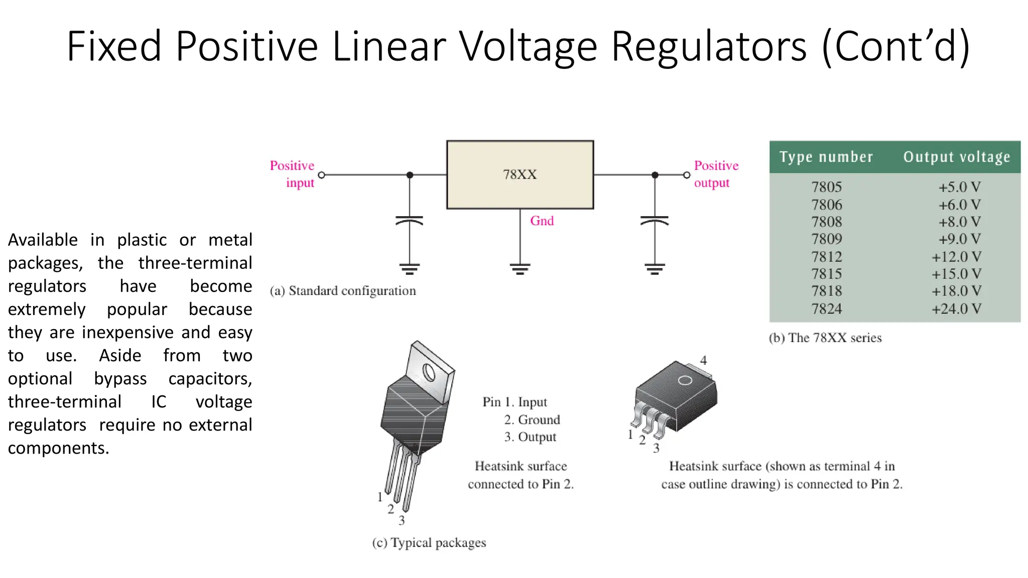
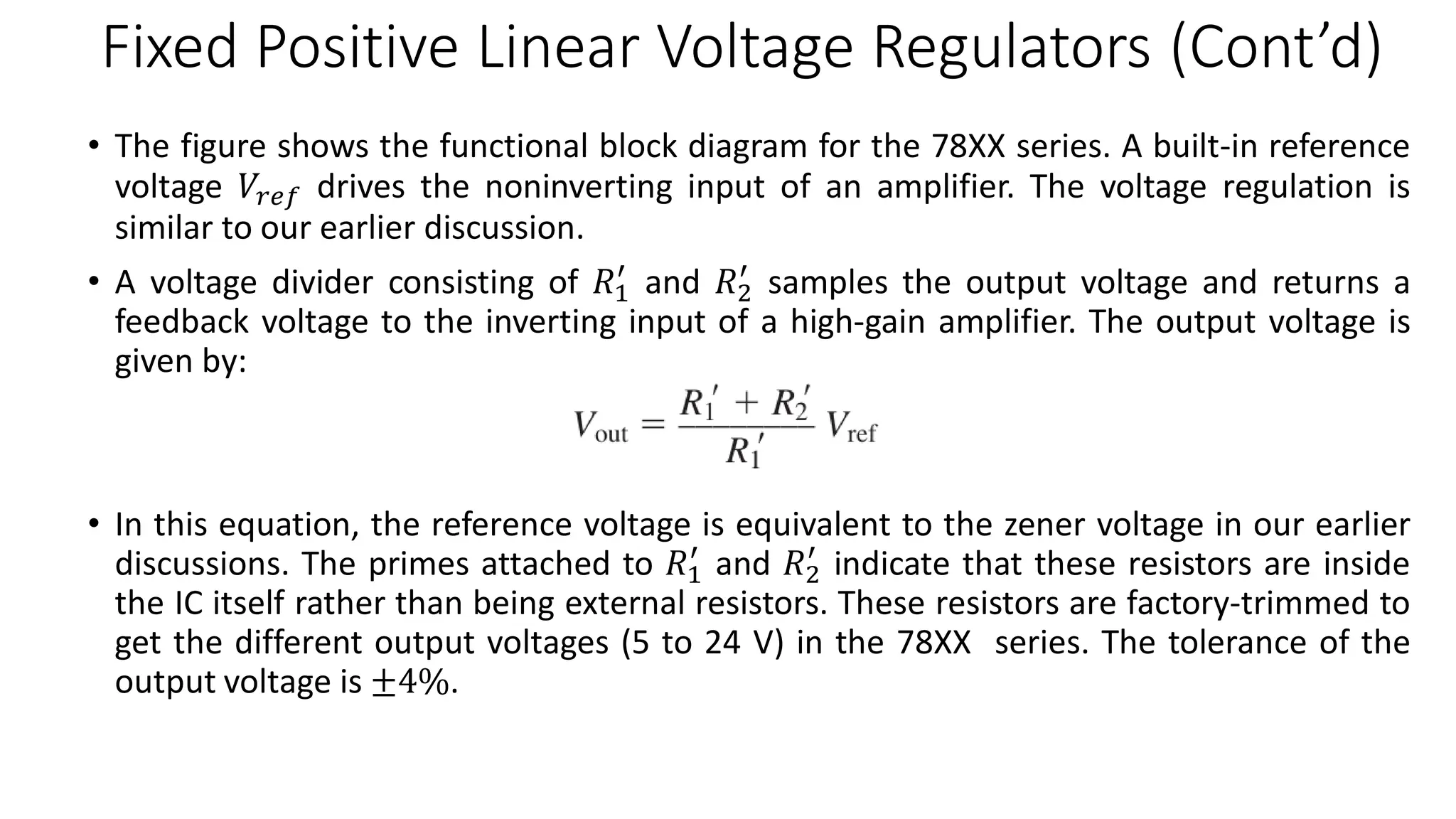
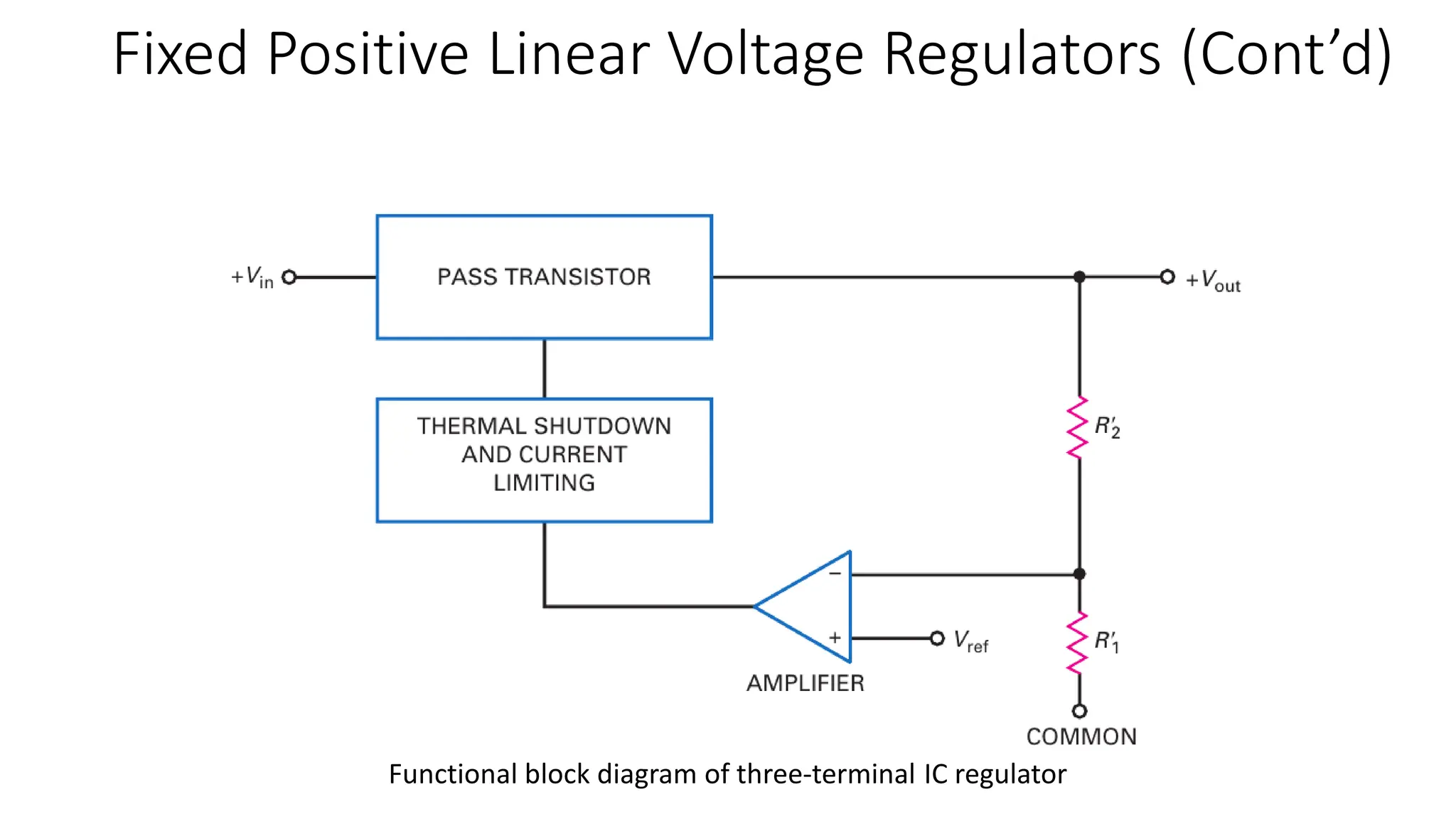
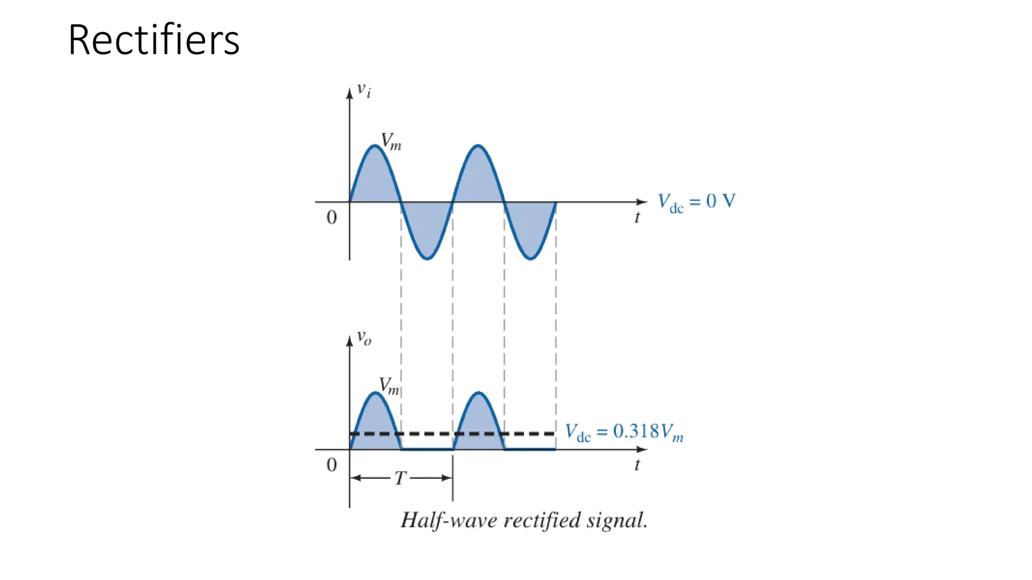
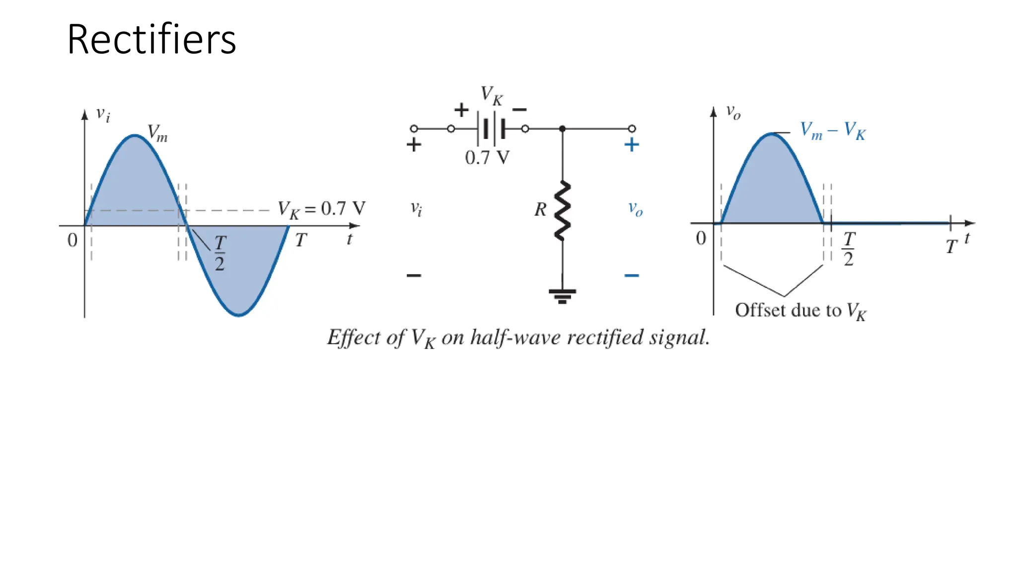
The document discusses various electronic components, including rectifiers, light-emitting diodes (LEDs), photodiodes, optocouplers, and fixed positive linear voltage regulators. It explains their operation, applications, and characteristics such as ripple voltage in rectification, light emission in LEDs, and electrical isolation in optocouplers. The text provides insights into the configuration and function of the 78xx series of voltage regulators, highlighting their reliability and ease of use.

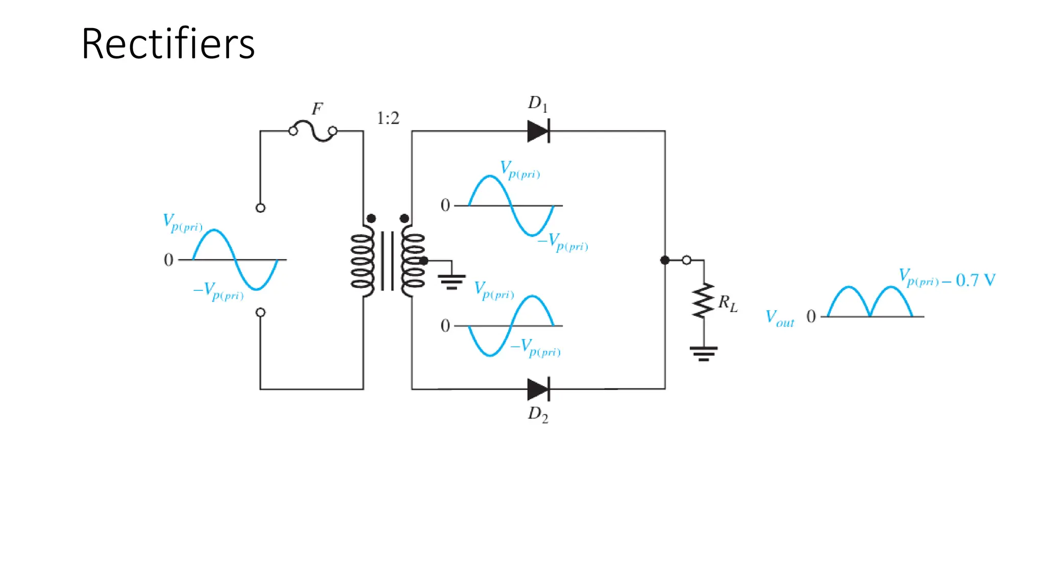
![Rectifiers
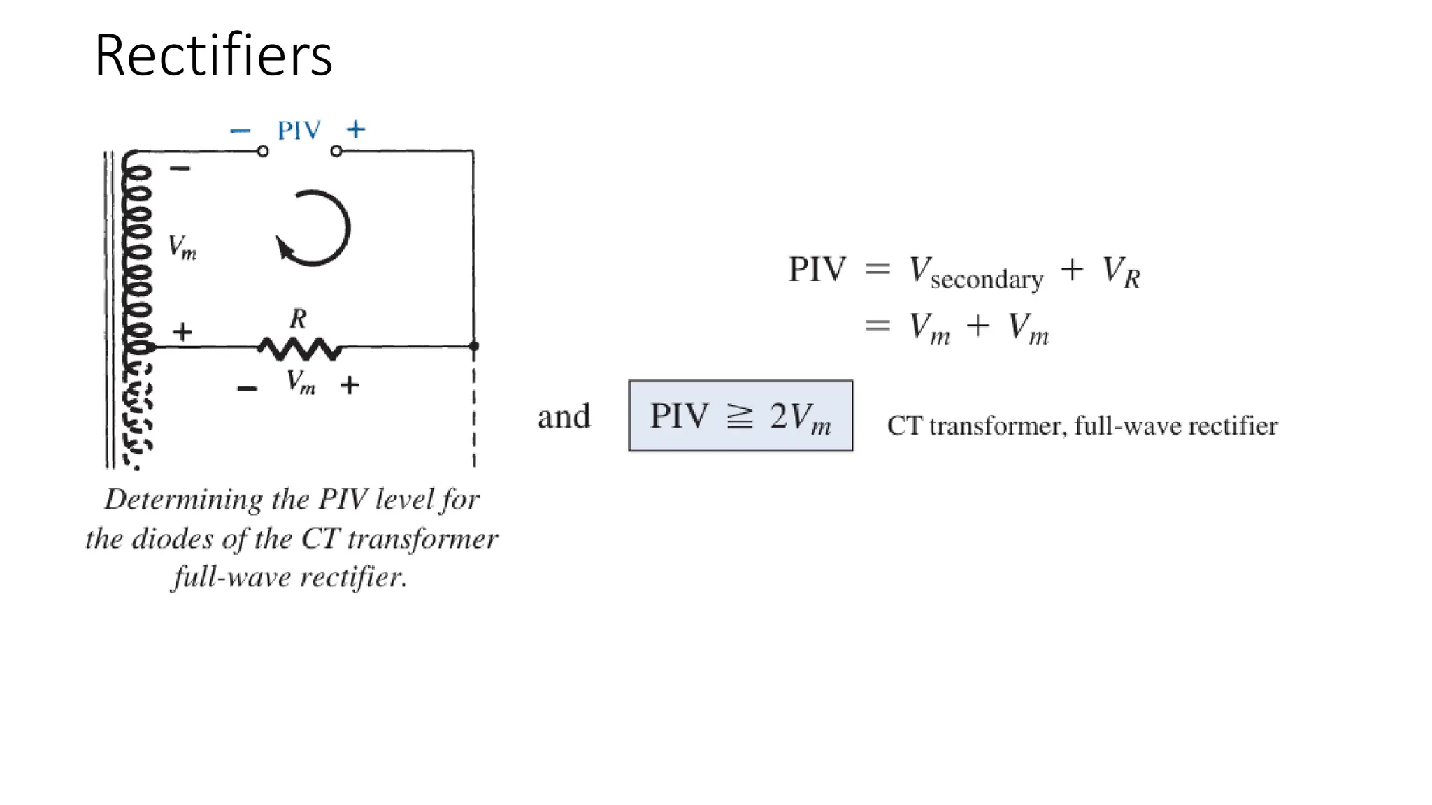
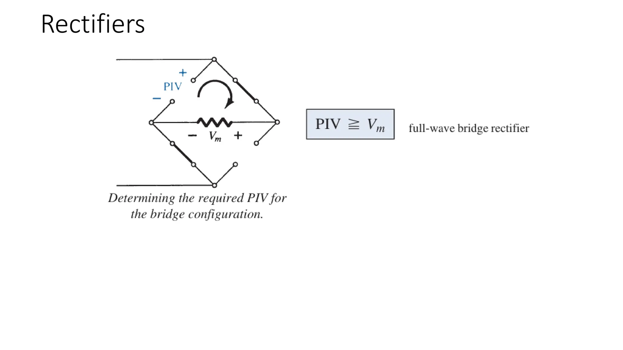
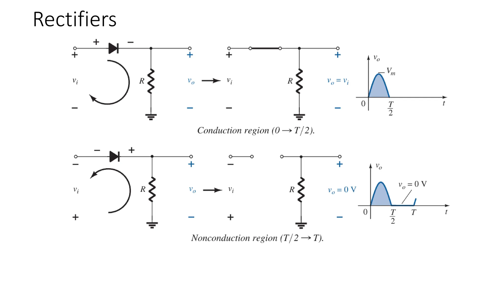
The peak inverse voltage (PIV) [or PRV (peak reverse voltage)] rating of the diode is of primary
importance in the design of rectification systems. Recall that it is the voltage rating that must
not be exceeded in the reverse-bias region or the diode will enter the Zener avalanche region.](https://image.slidesharecdn.com/rectifiersledphotodiodeandphotocoupler-250110134612-70a68e1a/75/Rectifiers-LED-Photodiode-and-Photocoupler-pdf-6-2048.jpg)