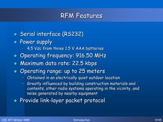
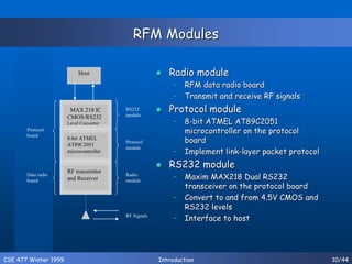
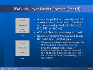
The document provides an overview of radio frequency (RF) data communications technology, focusing on its characteristics, regulations, and applications. It details the components of RF systems, such as transceivers, data radio boards, and protocol microcontrollers, along with their operations and interfaces. The document emphasizes low-power wireless communication capabilities, typical uses, and operational parameters like data rates and regulatory compliance.
![CSE 477 Winter 1999 Introduction 52/44
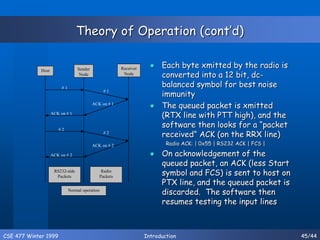
Sample Codes
RFSend(Byte ToFrom, Char* Data)
{
FIRST:
SerSend(ToFrom, 1);
SECOND:
begin = TimGetTicks();
do {
end = TimGetTicks();
SerReceiveCheck(&numBytes);
} while(numBytes < 0 && (end-begin/100) < .05);
THIRD:
if(numBytes > 0) {
SerReceive(rcvQueue, numBytes);
if(rcvQueue[0] == ToFrom) {
SerSend(pktNum, 1);
SerSend(StrLen(data), 1);
SerSend(data, StrLen(data));
FIRST:
Send ToFrom byte to RFM
SECOND:
Check to see if anything is
echoed back in 50ms
THIRD:
Check to see if this byte is the
ToFrom byte
If it is, then RFM is ready for
the rest of the packet: packet
number, data size, and actual
data; else, can assume that RFM
is busy.
Note: assume data size is less
than 32 bytes, which is the
maximum number of bytes that a
packet can take](https://image.slidesharecdn.com/rf-240428071144-8c8d6afa/85/Radio-frequency-data-communication-DT-ppt-52-320.jpg)
![CSE 477 Winter 1999 Introduction 53/44
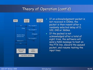
Sample Codes (cont’d)
FOURTH:
SerReceive(rcvQueue, 3);
switch(rcvQueue[2]) {
case 0xE1:
case 0xE2:
case 0xE3:
case 0xE4:
case 0xE5:
case 0xE6:
case 0xE7:
case 0xE8: if(++pktNum >= 8) pktNum = 1;
return true;
case 0xDD: return false;
}
}
}
return false;
}
FOURTH:
Receive the echo-back packet (3
bytes in size)
If the last byte is 0xEn where n =
1 - 8 (the number of retries),
then the packet is the ACK, and
data is successfully sent and
received; Else, if the last byte is
0xDD, it is the NAK, signaling a
link failure](https://image.slidesharecdn.com/rf-240428071144-8c8d6afa/85/Radio-frequency-data-communication-DT-ppt-53-320.jpg)
![CSE 477 Winter 1999 Introduction 54/44
Sample Codes (cont’d)
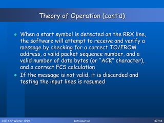
RFReceive(Byte localAddr, Byte* From, Byte* PktNum, Char*
retData)
{
FIRST:
SerReceiveCheck(&numBytes);
if (numBytes > 3) {
SerReceive(rcvQueue, 1);
SECOND:
if ((rcvQueue[0] >> 4) == localAddr) {
SerReceive(rcvQueue+1, 2);
*From = rcvQueue[0] & 0x0F; // Get FROM nibble
*PktNum = rcvQueue[1];
SerReceive(rcvQueue+3, rcvQueue[2]);
StrCopy(retData, rcvQueue+3);
return true;
}
}
return false;
}
FIRST:
Check the serial receive queue
to see whether at least 3
bytes have been received
(To/From, packet number,
packet size)
SECOND:
Get the first byte to see if it
is equal to the local node
address
If it is, get the next 2 bytes:
packet number and packet size,
and then get the rest of the
packet based on the packet
size received;
Else, do nothing](https://image.slidesharecdn.com/rf-240428071144-8c8d6afa/85/Radio-frequency-data-communication-DT-ppt-54-320.jpg)


