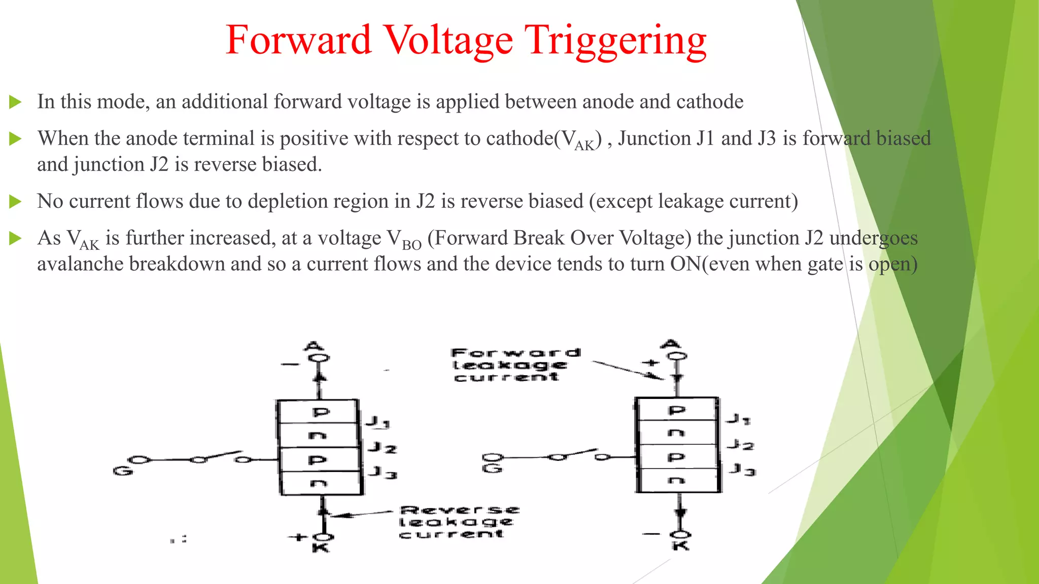
POWER SEMICONDUCTING SWITCHES
Delivered By :
Indubhushan Kumar
Assistant Professor -II
Department of Electrical Engineering
JECRC University , Jaipur
OVERVIEW
 Power Semiconducting Switch : Introduction
 Silicon Control Rectifier
 Thyristor Characteristics
 Protection
 Applications
Power Semiconductor Switches
o Broadly Classified into 3-Types : Power Diodes
: Power Transistors
: Thyristors
o Used to Control & Conversion of Electric Power
o Rated at Power Level rather than Signal Level
o Fast dynamic response
o Small Size & Less Maintenance
o Highly Efficient & Reliable
Thyristors Family
 Silicon controlled switch (SCR) : Unidirectional , 7000 V/ 5000 A , 1kHz
 Gate-turnoff thyristor (GTO) : Unidirectional , 5000V/ 3000A , 2kHz
 Triac : Bidirectional , 1200 V/ 1000 A, 0.5 kHz
 Silicon induction Thyristor (SITH) : Unidirectional , 2500 V/ 500 A , 100kHz
 Mos-controlled switch (MCT) : Unidirectional , 1200 V/ 40 A, 20 kHz
 ASCR /RCT : Bidirectional , 2500 V/ 400 A , 2 kHz
 LASCR : Unidirectional , 6000 V/ 3000 A, 1 kHz
Silicon Controlled Rectifier
 Most popular of thyristor family
 Commonly used in power electronic applications.
 3 terminals (Anode , cathode ,Gate ) , 4-layers switch
 Turned on by applying +ve gate signal when anode is +ve w.r.t cathode
 SCR is turned off by interrupting anode current
SCR Characteristic Curve
SCR Triggering (Turn-on) Methods
 The turning on Process of the SCR is known as Triggering.
 In other words, turning the SCR from Forward-Blocking state to Forward-Conduction
state is known as Triggering.
SCR Triggering Method
 Forward Voltage Triggering
 Thermal or Temperature Triggering
 Radiation or Light triggering
 dv/dt Triggering
 Gate Triggering
Forward Voltage Triggering
 In this mode, an additional forward voltage is applied between anode and cathode
 When the anode terminal is positive with respect to cathode(VAK) , Junction J1 and J3 is forward biased
and junction J2 is reverse biased.
 No current flows due to depletion region in J2 is reverse biased (except leakage current)
 As VAK is further increased, at a voltage VBO (Forward Break Over Voltage) the junction J2 undergoes
avalanche breakdown and so a current flows and the device tends to turn ON(even when gate is open)
Thermal Triggering
 The width of depletion layer of SCR decreases with increase in junction
temperature.
 when anode voltage is very near its breakdown voltage, the device is triggered by
increasing the junction temperature.
 By increasing the junction temperature the reverse biased junction collapses
thus the device starts to conduct.
Light Triggering
 For light triggered SCRs a special terminal niche is made inside the inner P layer
instead of gate terminal
 When light is allowed to strike this terminal, free charge carriers are generated.
 When intensity of light becomes more than a normal value, thyristor starts conducting
 This type of SCRs are called as LASCR
dv/dt Triggering
 When the device is forward biased, J1 and J3 are forward biased, J2 is reverse biased.
 Junction J2 behaves as a capacitor, due to the charges existing across the junction.
 If voltage across the device is V, the charge by Q and capacitance by C then,
ic = dQ/dt , Q = CV
ic = d(CV) / dt
= C. dV/dt + V. dC/dt ( as dC/dt = 0)
ic = C.dV/dt
 Therefore when the rate of change of voltage across the device
becomes large, the device may turn ON, even if the voltage across
the device is small.
Gate Triggering Method
 Most widely used SCR triggering method
 Applying a positive voltage between gate and cathode can Turn ON a forward
biased thyristor
 When a positive voltage is applied at the gate terminal, charge carriers are injected
in the inner P-layer, thereby reducing the depletion layer thickness
 As the applied voltage increases, the carrier injection increases, therefore the
voltage at which forward break-over occurs decreases
Contd…
Thyristor Protection
 For reliable operation of SCR, it should be operated within the specific ratings
 SCRs are very delicate devices and so they must be protected against abnormal
operating conditions. Various protection of SCR are
 di/dt Protection
 dv/dt Protection
 Over voltage Protection
 Over Current Protection
 Gate Protection
di/dt Protection
 local hot spots is created near the gate due to increased current density.
 This localised heating may damage the device.
 This is done by means of connecting an inductor in series with the thyristor.
dv/dt Protection
 We know that iC=C.dv/dt. ie, when dv/dt is high, iC is high.
 This high current(iC) may turn ON SCR even when gate current is zero. This is called as
dv/dt turn ON or false turn ON of SCR
 To protect the thyristor against false turn ON or against high dv/dt a "Snubber Circuit"
is used.
Overvoltage & OverCurrent Protection
 Overvoltage may result in false turn ON of the device (or) damage the device.
 The effect of overvoltage is reduced by using Snubber circuits and Non-Linear Resistors called Voltage
Clamping Devices
 In an SCR due to over-current, the junction temperature exceeds the rated value and the device gets
damaged.
 Over-current is interrupted by conventional fuses and circuit breakers
Gate Protection
o Gate circuit should be protected against Overvoltage & Overcurrent
o Protection against overvoltage is achieved by connecting Zener Diode across it
o A resistance is connected in series with Gate Circuit used to protect against Overcurrent
o Protection against Noise is done by connecting R-C across it.
Applications
 Traction Control of Electric Vehicles
 Switching Purpose
 HVDC Transmission Lines
 Excitation System
 Textile Miles
 Evevators
 Aerospace
 Trolley Bus etc ..
THANK YOU
GO GREEN

Power semiconducting switches

  • 1.
    POWER SEMICONDUCTING SWITCHES DeliveredBy : Indubhushan Kumar Assistant Professor -II Department of Electrical Engineering JECRC University , Jaipur
  • 2.
    OVERVIEW  Power SemiconductingSwitch : Introduction  Silicon Control Rectifier  Thyristor Characteristics  Protection  Applications
  • 3.
    Power Semiconductor Switches oBroadly Classified into 3-Types : Power Diodes : Power Transistors : Thyristors o Used to Control & Conversion of Electric Power o Rated at Power Level rather than Signal Level o Fast dynamic response o Small Size & Less Maintenance o Highly Efficient & Reliable
  • 5.
    Thyristors Family  Siliconcontrolled switch (SCR) : Unidirectional , 7000 V/ 5000 A , 1kHz  Gate-turnoff thyristor (GTO) : Unidirectional , 5000V/ 3000A , 2kHz  Triac : Bidirectional , 1200 V/ 1000 A, 0.5 kHz  Silicon induction Thyristor (SITH) : Unidirectional , 2500 V/ 500 A , 100kHz  Mos-controlled switch (MCT) : Unidirectional , 1200 V/ 40 A, 20 kHz  ASCR /RCT : Bidirectional , 2500 V/ 400 A , 2 kHz  LASCR : Unidirectional , 6000 V/ 3000 A, 1 kHz
  • 6.
    Silicon Controlled Rectifier Most popular of thyristor family  Commonly used in power electronic applications.  3 terminals (Anode , cathode ,Gate ) , 4-layers switch  Turned on by applying +ve gate signal when anode is +ve w.r.t cathode  SCR is turned off by interrupting anode current
  • 7.
  • 8.
    SCR Triggering (Turn-on)Methods  The turning on Process of the SCR is known as Triggering.  In other words, turning the SCR from Forward-Blocking state to Forward-Conduction state is known as Triggering.
  • 9.
    SCR Triggering Method Forward Voltage Triggering  Thermal or Temperature Triggering  Radiation or Light triggering  dv/dt Triggering  Gate Triggering
  • 10.
    Forward Voltage Triggering In this mode, an additional forward voltage is applied between anode and cathode  When the anode terminal is positive with respect to cathode(VAK) , Junction J1 and J3 is forward biased and junction J2 is reverse biased.  No current flows due to depletion region in J2 is reverse biased (except leakage current)  As VAK is further increased, at a voltage VBO (Forward Break Over Voltage) the junction J2 undergoes avalanche breakdown and so a current flows and the device tends to turn ON(even when gate is open)
  • 11.
    Thermal Triggering  Thewidth of depletion layer of SCR decreases with increase in junction temperature.  when anode voltage is very near its breakdown voltage, the device is triggered by increasing the junction temperature.  By increasing the junction temperature the reverse biased junction collapses thus the device starts to conduct.
  • 12.
    Light Triggering  Forlight triggered SCRs a special terminal niche is made inside the inner P layer instead of gate terminal  When light is allowed to strike this terminal, free charge carriers are generated.  When intensity of light becomes more than a normal value, thyristor starts conducting  This type of SCRs are called as LASCR
  • 13.
    dv/dt Triggering  Whenthe device is forward biased, J1 and J3 are forward biased, J2 is reverse biased.  Junction J2 behaves as a capacitor, due to the charges existing across the junction.  If voltage across the device is V, the charge by Q and capacitance by C then, ic = dQ/dt , Q = CV ic = d(CV) / dt = C. dV/dt + V. dC/dt ( as dC/dt = 0) ic = C.dV/dt  Therefore when the rate of change of voltage across the device becomes large, the device may turn ON, even if the voltage across the device is small.
  • 14.
    Gate Triggering Method Most widely used SCR triggering method  Applying a positive voltage between gate and cathode can Turn ON a forward biased thyristor  When a positive voltage is applied at the gate terminal, charge carriers are injected in the inner P-layer, thereby reducing the depletion layer thickness  As the applied voltage increases, the carrier injection increases, therefore the voltage at which forward break-over occurs decreases
  • 15.
  • 16.
    Thyristor Protection  Forreliable operation of SCR, it should be operated within the specific ratings  SCRs are very delicate devices and so they must be protected against abnormal operating conditions. Various protection of SCR are  di/dt Protection  dv/dt Protection  Over voltage Protection  Over Current Protection  Gate Protection
  • 17.
    di/dt Protection  localhot spots is created near the gate due to increased current density.  This localised heating may damage the device.  This is done by means of connecting an inductor in series with the thyristor.
  • 18.
    dv/dt Protection  Weknow that iC=C.dv/dt. ie, when dv/dt is high, iC is high.  This high current(iC) may turn ON SCR even when gate current is zero. This is called as dv/dt turn ON or false turn ON of SCR  To protect the thyristor against false turn ON or against high dv/dt a "Snubber Circuit" is used.
  • 19.
    Overvoltage & OverCurrentProtection  Overvoltage may result in false turn ON of the device (or) damage the device.  The effect of overvoltage is reduced by using Snubber circuits and Non-Linear Resistors called Voltage Clamping Devices  In an SCR due to over-current, the junction temperature exceeds the rated value and the device gets damaged.  Over-current is interrupted by conventional fuses and circuit breakers
  • 20.
    Gate Protection o Gatecircuit should be protected against Overvoltage & Overcurrent o Protection against overvoltage is achieved by connecting Zener Diode across it o A resistance is connected in series with Gate Circuit used to protect against Overcurrent o Protection against Noise is done by connecting R-C across it.
  • 21.
    Applications  Traction Controlof Electric Vehicles  Switching Purpose  HVDC Transmission Lines  Excitation System  Textile Miles  Evevators  Aerospace  Trolley Bus etc ..
  • 22.