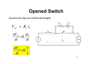
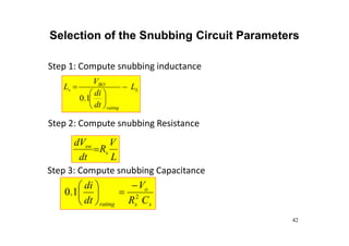
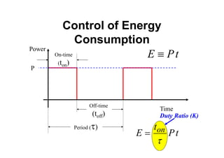
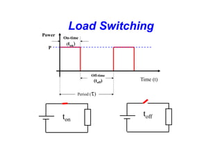
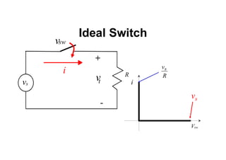
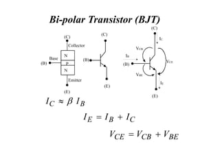
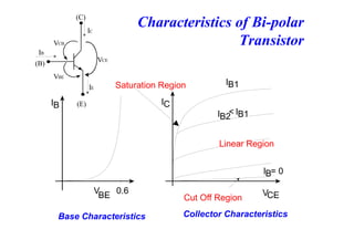
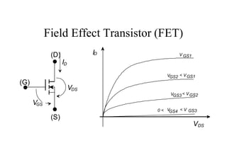
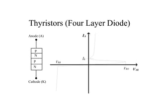
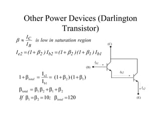
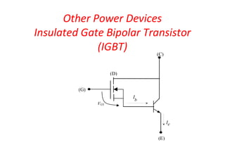
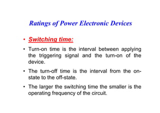
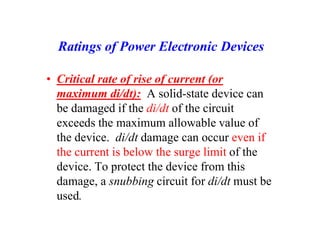
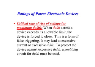
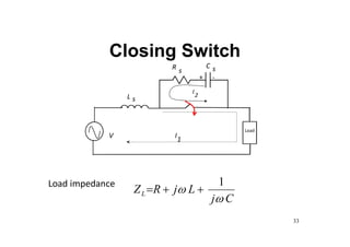
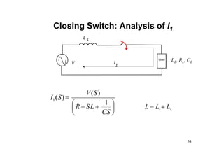
This document discusses power electronic devices and their characteristics. It describes several types of power devices including bipolar junction transistors (BJT), field effect transistors (FET), thyristors, Darlington transistors, and insulated gate bipolar transistors (IGBT). It covers the key characteristics, operating principles, and ratings of these devices. It also discusses how snubber circuits using inductors, resistors, and capacitors can be designed to protect power devices from high rates of change of current (di/dt) and voltage (dv/dt) during switching.

![Thyristors [Silicon Controlled Rectifier
(SCR)]
AK
VBO
I
A
V
VRB
Anode (A)
Cathode (K)
Gate (G)
V
TO
Ig > 0
Ig = 0
Ig = max
Ih](https://image.slidesharecdn.com/powerelectronicsdevicesandtheircharacteristics-220114182638/85/Power-electronics-devices-and-their-characteristics-15-320.jpg)
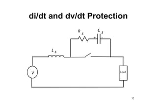
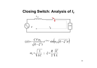
![Snubbing Circuit: Ls
]
)
1
(
[
cos
]
)
1
(
[
sin
)
1
(
2
2
2
2
2
1
t
e
V
C
t
e
V
C
dt
di
n
t
n
n
t
n n
n
L
V
dt
di
max
1
Worst Scenario for Maximum di/dt: When the load capacitor is not charged at t=0
L
s L
dt
di
V
L
max
1
L
rating
BO
s L
dt
di
V
L
1
.
0
2
max
1
n
V
C
dt
di
36
LC
n
1
](https://image.slidesharecdn.com/powerelectronicsdevicesandtheircharacteristics-220114182638/85/Power-electronics-devices-and-their-characteristics-36-320.jpg)