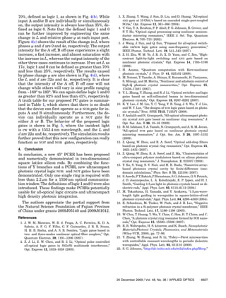
This document proposes and analyzes photonic NOT and NOR logic gates based on a single photonic crystal ring resonator (PCRR). The PCRR is formed by removing rods along the ΓM direction in a square lattice photonic crystal structure. Beam interference theory and 2D FDTD simulations are used to analyze the logic gate behavior. The simulations show the gates can function as NOT and NOR gates without requiring nonlinear materials. An output intensity greater than 50% is defined as logic 1, and less than 50% as logic 0. This approach could potentially be used to integrate photonic logic circuits on a chip.
MINIATURIZATION OF BRANCH-LINE COUPLERS USING OPEN STUBS AND STEPPED IMPEDANC...csijjournal
The document summarizes two proposed structures for compact branch-line couplers (BLCs) using miniaturization techniques. The first structure uses open stubs and meandering transmission lines, reducing the area to 61.8% of a conventional design. The second uses open stub and stepped impedance unit cells, reducing the area to 50.8%. Simulation results show the first structure achieves return losses and isolation of -27.8 dB and -27.9 dB respectively with a 312 MHz bandwidth. The second structure achieves comparable performance to previously published measured results. Both miniaturized designs achieve good size reduction while maintaining BLC performance compared to a conventional design.
International Journal of Engineering Research and Applications (IJERA) is an open access online peer reviewed international journal that publishes research and review articles in the fields of Computer Science, Neural Networks, Electrical Engineering, Software Engineering, Information Technology, Mechanical Engineering, Chemical Engineering, Plastic Engineering, Food Technology, Textile Engineering, Nano Technology & science, Power Electronics, Electronics & Communication Engineering, Computational mathematics, Image processing, Civil Engineering, Structural Engineering, Environmental Engineering, VLSI Testing & Low Power VLSI Design etc.
Welcome to International Journal of Engineering Research and Development (IJERD)IJERD Editor
This document summarizes research on novel photonic crystal fiber (PCF) structures with elliptical holes whose dimensions are derived from Dolph Tschebysheff polynomials. Three new PCF structures are proposed and their propagation characteristics are analyzed using simulations. The simulations show that the proposed structures exhibit negligible waveguide dispersion over a wide wavelength range, making them suitable for long distance communications. However, the birefringence of the structures is higher than PCF structures based on Pascal's triangle. The confinement losses of the proposed structures are also slightly higher. In conclusion, the PCF structures derived from Dolph Tschebysheff polynomials show potential for applications requiring low dispersion, but have increased birefringence and losses compared
Design of a Selective Filter based on 2D Photonic Crystals Materials IJECEIAES
Two dimensional finite differences temporal domain (2D-FDTD) numerical simulations are performed in cartesian coordinate system to determine the dispersion diagrams of transverse electric (TE) of a two-dimension photonic crystal (PC) with triangular lattice. The aim of this work is to design a filter with maximum spectral response close to the frequency 1.55 μm. To achieve this frequency, selective filters PC are formed by combination of three waveguides W 1 K A wherein the air holes have of different normalized radii respectively r 1 /a=0.44, r 2 /a=0.288 and r /a= 0.3292 (a: is the periodicity of the lattice with value 0.48 μm). Best response is obtained when we insert three small cylindrical cavities (with normalized radius of 0.17) between the two half-planes of photonic crystal strong lateral confinement.
The document discusses a new method for evaluating interactions in the method of moments (MoM) for antennas printed on ultra-thin substrates. It first presents the scalar Green's functions and their asymptotic forms for ultra-thin substrates. It then describes using the Kummer principle to extract the asymptotic Green's functions from the total Green's functions to calculate the Z impedance matrix in the MoM. Validation and numerical results are presented to demonstrate advantages in terms of time consumption. The goal is to develop a robust treatment of antennas on very thin substrates to enable applications in areas like printed electronics and sensors.
The document discusses simulation and testing of antennas for 4G LTE-MIMO systems. It describes simulating a PIFA antenna in CST Studio Suite to compare matched and unmatched cases. Results showed improved return loss and far-field patterns when the antenna was matched. Testing of a MIMO antenna system involved measuring isolation between antennas and comparing performance with the enclosure open versus closed.
Ieee 802.20 working group on mobile broadband wireless accessNguyen Minh Thu
This document discusses inconsistencies in the path loss models recommended for evaluating mobile broadband wireless access (MBWA) proposals for the IEEE 802.20 working group. It proposes additions to clarify the frequency dependence of the path loss models for different environments (macrocell suburban/urban, microcell LOS/NLOS, indoor). Models are provided for path loss as a function of carrier frequency and distance. It recommends adopting the proposed path loss formulations and accounting for carrier frequency and bandwidth when evaluating proposals using different channel models.
Design and simulation of broadband rectangular microstrip antennaBASIM AL-SHAMMARI
Abstract
In this work, many techniques are suggested and analyses for
rectangular microstrip antenna (RMSA) operating in X-band for 10 GHz
center frequency. These approaches are: lowering quality factor, shifting
feeding point , using reactive loading and modification of the patch shape.
The design of a RMSA is made to several dielectric materials, and the
selection is based upon which material gives a better antenna performance
with reduced surface wave loss. Duroid 5880 and Quartz are the best materials
for proposed design to achieve a broader Bandwidth (BW) and better
mechanical characteristics than using air. The overall antenna BW for RMSA
is increased by 11.6 % with Duroid 5880 with shifted feeding point and with
central shorting pin (Reactive loading) while that for Quartz is 17.4 %.
Modification of patch shape with similar improving techniques gives an
overall increasing VSWR bandwidth of 26.2 % for Duroid 5880 and a
bandwidth of 30.9 % for Quartz. These results are simulated using Microwave
Office package version 3.22, 2000.
This document describes a simulation of an optical orthogonal frequency division multiplexing (OFDM) system using different M-ary quadrature amplitude modulation (QAM) techniques. The performance of the system was evaluated in terms of bit error rate (BER) and signal-to-noise ratio (SNR) by varying the modulation order M to 16, 64, and 256. Simulation results showed that higher modulation orders require higher SNR values to achieve the same BER as lower modulation orders. The simulated results closely matched theoretical predictions, though there was a deviation of 3-3.5 dB, likely due to additional noise and losses not accounted for in the theoretical model.
Scattering Regimes for Underwater Optical Wireless Communications using Monte...IJECEIAES
Optical wireless communications has shown tremendous potential for underwater applications as it can provide higher bandwidth and better security compared to acoustic technologies. In this paper, an investigation on scattering regimes for underwater links using Monte Carlo simulation has been presented.While the focus of this paper is on diffuse links, the simulation results of collimated links is also provided for comparison purpose. Three types of water namely clear, coastal and turbid water are being used in the simulation. It is shown that the effect of scattering on the path loss cannot be accurately modeled by the existing channel model; ie. Beers-Lambert (BL) law. It has been shown that the distance at which the unscattered light drops to zero can be used to estimate the transition point for the scattering regimes in case of diffuse links. The transition point for diffuse links in coastal water and turbid water can be estimated to be around 22 m and 4 m respectively. Further analysis on the scattering order probability at different scattering regimes illustrates how scattering is affected by beam size, water turbidity and distance. From the frequency response plot, it is estimated that the bandwidth of several order of GHz can be achieved when the links are operating in the minimal scattering region and will reduce to several hundreds of MHz when the link is operating in multiple scattering region.
Miniaturized Minkowski-Island Fractal Microstrip Antenna Fed by Proximity Cou...TELKOMNIKA JOURNAL
This paper proposed a new design of Minkowski Island microstrip antenna fed by proximity coupling with partial ground plane. The design was consisted of two layers of substrate, on the top substrate was the antenna patch and on the bottom substrate was the proximity feed line and the partial ground. At the first stage, the normal square patch antenna was mainly designed. Then, the Minkowski patch antenna was designed using 1st iteration technique and 2nd iteration technique. The Minkowski fractal shape slot was embedded in the center of the patch to form a Minkowski Island patch antenna. Using the Minkowski Island fractal technique, the dimension of the patch can be reduced up to 58.7%. The proximity feed line in this design was used to increase the impedance bandwidth, and from the measurement the impedance bandwidth of the proposed antenna was 240 MHz with return loss of -24.54 dB and VSWR of 1.126.
Enhanced Mobile Node Tracking With Received Signal Strength in Wireless Senso...IOSR Journals
Node localization is important parameter in WSN. Node localization is required to report origin of
events which makes it one of the important challenges in WSN. Received signal strength (RSS) is used to
calculate distance between mobile node and reference node. The position of the mobile node is calculated using
multilateration algorithm (MA). Extended Kalman filter (EKF) is utilized to estimate the actual position. In this
paper, the implementation and enhancement of a tracking system based on RSS indicator with the aid of an
Extended Kalman Filter (EKF) is described and an adaptive filter is derived.
This paper presents a trifocal Rotman Lens Design
approach. The effects of focal ratio and element spacing on
the performance of Rotman Lens are described. A three beam
prototype feeding 4 element antenna array working in L-band
has been simulated using RLD v1.7 software. Simulated
results show that the simulated lens has a return loss of –
12.4dB at 1.8GHz. Beam to array port phase error variation
with change in the focal ratio and element spacing has also
been investigated.
This paper summarizes research on using fiber Bragg gratings (FBG) for dispersion compensation in a 10 Gbps optical communication system using return-to-zero (RZ) modulation format. Simulation results showed that using an FBG to compensate for dispersion in a 3200 km long single mode fiber transmission link improved the bit error rate and Q-factor. Eye diagrams taken at 100 km, 1600 km, and 3200 km after dispersion compensation by the FBG demonstrated reduced pulse spreading and improved eye openings compared to the uncompensated case. The FBG provided effective dispersion compensation to improve transmission performance over long distances.
Investigation of optimal duty cycle for gvd undercompensatedIAEME Publication
This document summarizes an investigation into optimizing the duty cycle of input pulses in an undercompensated optical fiber link. The link consists of 5 loops, each with 50km of standard single mode fiber followed by dispersion compensating fiber. Simulation results show that higher duty cycle pulses (66-75%) permit greater undercompensation (up to 1.3% reduction in dispersion compensating fiber length) while maintaining reliable communication compared to lower duty cycle pulses (25-33%) which only tolerate up to 1% undercompensation. The optimal duty cycle balances fiber nonlinearities and accumulated dispersion to maximize the quality factor over the greatest range of input powers for a given level of undercompensation.
This document proposes and evaluates scheduling frameworks for optical integrated interconnection networks (ONoC) to address limitations of electrical interconnects like power dissipation and latency. It presents a two-step scheduling approach involving maximum weight matching for packet scheduling and first-fit wavelength assignment. Simulation results show tunable transmitters and ring topologies achieve better performance than fixed transmitters and bus topologies. Maximum weight matching also outperforms iSLIP scheduling. Future work may explore bidirectional topologies and other scheduling frameworks.
The document describes two unique photonic crystal fiber (PCF) designs shaped like an S and a U. The S-shaped PCF exhibits zero dispersion at three points within the third optical window, while the U-shaped PCF has zero dispersion at the first optical window. Both designs show birefringence on the order of 10-5 and confinement loss on the order of 10-3. Simulation results show the S-shaped PCF has more suitable properties for applications like sensing.
Realization of Dual-Dipole-Antenna System for Concurrent Dual-Radio Operation...Saou-Wen Su
The document proposes a dual-dipole-antenna system for concurrent dual-radio operation at 2.4 GHz and 5 GHz bands. It first studies the mutual coupling between two dipole antennas and finds good isolation when the antennas are orthogonal in polarization. Based on this, the design places a 2.4 GHz dipole perpendicular to a 5 GHz dipole on a two-layer substrate. Simulations show the antennas, stacked just 0.8 mm apart, achieve over 15 dB isolation across bands. Measurements of a prototype confirm bandwidth and radiation pattern specifications for both WiFi standards are met while maintaining low coupling between closely packed antennas.
Band Clustering for the Lossless Compression of AVIRIS Hyperspectral ImagesIDES Editor
Hyperspectral images can be efficiently compressed
through a linear predictive model, as for example the one
used in the SLSQ algorithm. In this paper we exploit this
predictive model on the AVIRIS images by individuating,
through an off-line approach, a common subset of bands, which
are not spectrally related with any other bands. These bands
are not useful as prediction reference for the SLSQ 3-D
predictive model and we need to encode them via other
prediction strategies which consider only spatial correlation.
We have obtained this subset by clustering the AVIRIS bands
via the clustering by compression approach. The main result
of this paper is the list of the bands, not related with the
others, for AVIRIS images. The clustering trees obtained for
AVIRIS and the relationship among bands they depict is also
an interesting starting point for future research.
Very-Low-Cost Copper-Wire Antenna for 2.4-GHz WLAN OperationSaou-Wen Su
A very-low-cost copper-wire antenna, easily fabricated by bending a single 70-mm-long copper wire two times, for WLAN operation in the 2.4 GHz band (2400-2484 MHz) is presented. The antenna has a very simple structure and is easily fed by using a 50- mini-coaxial cable. A prototype of the proposed antenna with the overall dimensions 40 mm x 5 mm is constructed and tested.
This document discusses the effects of time offset (TO) and carrier frequency offset (CFO) on orthogonal frequency division multiplexing (OFDM) systems and proposes interference cancellation techniques. It introduces the OFDM system model and how CFO causes loss of orthogonality between subcarriers, resulting in inter-carrier interference (ICI) that degrades performance. The paper proposes an ICI reduction scheme using self-cancellation and evaluates its performance compared to standard OFDM. It also discusses using space-time block coding (STBC) with OFDM to improve performance by reducing bit error rate (BER) under different signal-to-noise ratios. Simulation results show STBC effectively mitigates the effects of inter-
International Journal of Engineering (IJE) Volume (2) Issue (3)CSCJournals
This document summarizes the analysis and design of a Hilbert curve fractal antenna with a coplanar waveguide feed for multi-band wireless communications. The authors designed and simulated a small Hilbert curve fractal antenna using simulation software. They analyzed the antenna using concepts of coplanar waveguide transmission lines and the mathematical definition of fractals to develop electromagnetic and empirical models. These models can predict the antenna's multi-resonance frequencies. Based on experiments, the electromagnetic model had a lower percent difference from experimental results compared to the empirical model, because it used a transmission line model while the empirical model used numerical methods. The models developed will help with the design and fabrication of Hilbert curve fractal antennas.
This document describes the design and analysis of a novel hexagonal lattice photonic crystal fiber with circular air holes to achieve low confinement loss and low chromatic dispersion. A fiber is designed with four rings of circular air holes with a radius of 0.8 μm, lattice pitch of 2.3 μm, and silica core. Finite difference time domain analysis shows this design achieves low confinement loss below 1 dB/km from 0.8-1.4 μm for both TE and TM modes. Dispersion is also flattened and near-zero from 0.8-1.3 μm. This novel fiber design optimizes parameters to gain low confinement loss and flattened dispersion over a wide wavelength range.
In this research paper, substrate integrated waveguide (SIW) was proposed as a technique by
realizing bilateral edge walls to produce a compact 5G beam-steering antenna at 24 GHz. The beam
forming network is produced using SIW directional coupler perform as 2×2 Butler Matrix (BM) fed with SIW
slotted waveguide antenna array. The output signal is steered from -29 degrees and +29 degrees when
the signal is fed to the respective input ports. If one of the input ports is fed, the signal is evenly distributed
between the adjacent output ports with 90 degree constant phase shift. The compact size of directional
coupler was designed by longitude slots on the surface of SIW substrate with bandwith of 16.85% at the
operating frequency. The proposed antenna produce gain of 6.34 dB at operating frequency and the
promising outcome of the beam steering make proposed design suitable for 5G communications especially
with tracking capabilities.
Analysis of Highly Birefringent Photonic Crystal Fiber Employing Different Ge...ijsrd.com
In this paper we are proposed three different types of photonic crystal fibers and compared them for higher birefringence by using finite element method. Using elliptical holes instead of circular air holes we are getting high birefringence. We also obtained low dispersion for the same structure consist of a defect in the center design flexibility and high index contrast give a better birefringence in the range of 10-3 to 10-2.Also the characteristics of PCF are plotted for a range of wavelength
This document discusses full dimension MIMO (FD-MIMO) technology for LTE-Advanced and 5G networks. It provides an overview of 3GPP activities related to FD-MIMO, including the recently completed 3D channel model, ongoing studies of FD-MIMO scenarios and antenna architectures. FD-MIMO uses a base station with a 2D active antenna array to support multi-user beamforming in both the elevation and azimuth dimensions, resulting in significantly higher cell capacity compared to conventional systems. The document also discusses challenges of reducing channel state information feedback overhead for large FD-MIMO systems.
Silicon Photonics and Photonic NoCs: A Surveydrv11291
This document summarizes a survey on silicon photonics and photonic Networks-on-Chip (NoCs). It discusses why photonic interconnects could replace metallic interconnects due to issues like RC delays and data transfer rates. It describes early work on the idea of silicon photonics and how photonic NoCs would affect router structures and architectures. The document summarizes several proposed photonic NoC architectures, routers, and simulation tools. It discusses tradeoffs between latency, throughput, and power for different architectures. While photonic NoCs show potential for improved performance, the document concludes that design and fabrication tools still need development before they can be considered practically viable for multi-core systems-on-chips.
This document summarizes a research paper about the development of a ground plane aperture technique to enhance capacitive coupling in parallel-coupled microstrip lines (PCMLs) and enable the design of broadband multi-pole microstrip bandpass filters. The technique involves forming an aperture in the ground plane of the PCML. Equivalent circuit models of the PCML indicate that the aperture increases the coupling factor in a frequency-dependent manner. A novel multi-pole broadband filter topology is proposed using a single microstrip line resonator connected between two PCML sections. Predicted and measured results confirm attractive properties such as 60% bandwidth, deep stop-band rejection, and compact size.
International Journal of Engineering Research and Applications (IJERA) is a team of researchers not publication services or private publications running the journals for monetary benefits, we are association of scientists and academia who focus only on supporting authors who want to publish their work. The articles published in our journal can be accessed online, all the articles will be archived for real time access.
Our journal system primarily aims to bring out the research talent and the works done by sciaentists, academia, engineers, practitioners, scholars, post graduate students of engineering and science. This journal aims to cover the scientific research in a broader sense and not publishing a niche area of research facilitating researchers from various verticals to publish their papers. It is also aimed to provide a platform for the researchers to publish in a shorter of time, enabling them to continue further All articles published are freely available to scientific researchers in the Government agencies,educators and the general public. We are taking serious efforts to promote our journal across the globe in various ways, we are sure that our journal will act as a scientific platform for all researchers to publish their works online.
Non-radiative wireless energy transfer with single layer dual-band printed sp...journalBEEI
Accomplishing equilibrium in terms of transfer efficiency for dual-band wireless energy transfer (WET) system remains as one of key concerns particularly in the implementation of a single transmitter device which supports simultaneous energy and data transfer functionality. Three stages of design method are discussed in addressing the aforementioned concern. A single layer dual-band printed spiral resonator for non-radiative wireless energy transfer operating at 6.78 MHz and 13.56 MHz is presented. By employing multi-coil approach, measured power transfer efficiency for a symmetrical link separated at axial distance of 30 mm are 72.34% and 74.02% at the respective frequency bands. When operating distance is varied between 30 mm to 38 mm, consistency of simulated peak transfer efficiency above 50% is achievable.
Theoretical Analysis of a two-stage Sagnac loop filter Using Jones Matrices IJECEIAES
In this work, a theoretical analysis of a Sagnac loop filter (SLF) with twostage polarization maintaining fibers (PMFs) and polarization controllers (PCs) is presented. The transmission function of this two-stage SLF is calculated in detail by using Jones matrix. The calculation is performed in order to investigate the filtering characteristics. The theoretical results show that the wavelength interval is depending on the dynamic settings of the length of the PMFs and the polarization angle of the PCs. By changing the polarization angle of the PCs, a multiple of single, dual or triple wavelength in each channel can be achieved. Based on this study, a flat multiwavelength spectrum can be obtained by adjusting the PMFs and the PCs in the twostage SLF. This finding significantly contributes to the generation of multiwavelength fiber laser (MWFL) that can be used for many optical applications.
MICROSTRIP COUPLED LINE FILTER DESIGN FOR ULTRA WIDEBAND APPLICATIONSjmicro
A compact microstrip parallel coupled line filter for ultra wide band applications by means of combining a network of coupled line and defected ground is proposed. The design equations for three and five interconnected networks are derived and implemented. Simulations for three different configurations for filters are optimized. Then three prototype circuits are constructed, a bandpass filter with center frequency 2.25 GHz and two different bandpass filters (in terms of perturbations) with center frequencies 2.33GHz.
For 2.25 GHz circuit wide fractional bandwidth of about 90% is obtained but undesired high return loss existed. For 2.33GHz circuit with grooves in sides fractional bandwidth of about 60% is obtained at about 3.4 GHz center frequency. However undesired return loss existed for this circuit whereas good out off or 2.33GHz circuit with grooves in whole sections the center frequency got shifted to about 3.4 GHz and about 50% fractional bandwidth is obtained with very good out off band performance observed.
In this paper, a low pass filter based on T-Shaped resonator is presented. The T-Shaped resonator consists of meandered lines and rectangular patches. Also, the LC model and transfer function of the proposed resonator is presented. For suppression of spurious harmonics, a bandstop structure consists of hexangular patches and open stubs has been utilized. Finally, the wide stopband microstrip lowpass filter with cutoff frequency 2.72 GHz has been simulated, fabricated and measured. The LPF has good characteristics such as wide stopband and insertion loss lower than 0.18 dB in the passband region. The rejection level is less than -20 dB from 2.98 up to 21.3 GHz. The filter size is 10.5 mm×12.7 mm, or 0.131 λg× 0.158 λg, where λg is the guided wavelength. The measured and simulated results of the filter is in good agreement with each other, which show the merits of low insertion loss and wide stopband.
Improving Splitting Efficiency in Photonic Crystal WaveguideIJERA Editor
“Photonic Crystals (PCs)” are dielectric structures with periodic spatial alternations of refractive index on the
scale of the wavelength of light. Many optical devices, based on PCs, have been proposed. There are
multiple ways by which equal amount of power of incoming signals can be divided into two, three and
four output channels; for example using multiple coupled photonic crystal waveguides, directional coupling and
cascaded multimode PC waveguides. Ideally, the splitter should divide the input power equally into the output
channels without significant reflection or radiation losses and should be compact in size. In this thesis I
have proposed the optical power splitting using Y-junction. The optical modeling of this proposed structure
was investigated by finite difference time domain (FDTD) simulation. The goal was to achieve equal power at
each output channel with broad spectrum around the target wavelength with low loss.
Analysis of dual core hexagonal pcf based polarization beam splitterAlexander Decker
This document analyzes the design and performance of polarization beam splitters based on dual core hexagonal photonic crystal fiber (PCF). The analysis uses finite element methods to calculate the effective refractive indices and coupling lengths of the even and odd supermodes for orthogonal polarizations. Numerical results show that coupling lengths increase with larger air hole diameters, and decrease with increasing operating wavelength. The analysis demonstrates that an 8.4 mm polarization beam splitter can achieve an extinction ratio of 250dB. This simple design of PCF polarization beam splitters may allow for easier fabrication while maintaining good performance.
This document describes two techniques for designing optical XNOR and NAND logic gates. The first technique uses a 2D array of coupled optical cavities with Kerr nonlinearity. Discrete cavity solitons are numerically simulated and used to demonstrate optical XNOR and NAND gates by controlling soliton interactions with a Gaussian beam. The second technique uses multi-mode interference waveguides to convert the phase of binary-phase-shift keying input signals to amplitude at the output, implementing optical XNOR and NAND logic. Numerical simulations using the finite element method show contrast ratios of 21.5 dB for the XNOR gate and 22.3 dB for the NAND gate.
Lantiq/Intel Contributions to G.fast at Scientific ConferencesLantiq
This document summarizes research on achievable data rates for hybrid copper/fiber networks using G.fast technology. It finds that linear precoding methods like zero-forcing perform well for shorter copper line lengths, while nonlinear methods have advantages for longer lines. The work analyzes performance losses from implementation limitations and proposes optimizing the transmit spectrum to improve achievable rates by incorporating these limitations into the optimization process. Rate-reach curves are generated based on a statistical channel model and constraints from the G.fast standard.
Design and manufacturing of iris waveguide filters for satellite communicationTELKOMNIKA JOURNAL
We propose in this paper, two bandpass filters in waveguide technology having rectangular symmetrical discontinuities with a half-radius r, designed and operating respectively in the X-Band (9-11.5) GHz and C-Band (3.5-5.5) GHz. These filters consists of eight irises placed symmetrically respectively on standard rectangular waveguides WR90 and WR229 in which resonant irises are inserted. These irises are used to couple the sections very strongly in this filter, which allows the bandwidth to be increased and the matching to be controlled. The comparison between the numerical and electromagnetic results, which we obtained for the filters, constitutes a means of validation of computer simulation technology (CST) environment and Mician for the design of the other circuit elements in the various frequency bands. We observed excellent consistency between the simulation curves and those of the measurements. The results obtained are promising and pave the way for the use of these structures in the fields of telecommunications.
International Journal of Engineering Research and Applications (IJERA) is an open access online peer reviewed international journal that publishes research and review articles in the fields of Computer Science, Neural Networks, Electrical Engineering, Software Engineering, Information Technology, Mechanical Engineering, Chemical Engineering, Plastic Engineering, Food Technology, Textile Engineering, Nano Technology & science, Power Electronics, Electronics & Communication Engineering, Computational mathematics, Image processing, Civil Engineering, Structural Engineering, Environmental Engineering, VLSI Testing & Low Power VLSI Design etc.
Design and optimization of microstrip filtering antenna with modified shaped ...TELKOMNIKA JOURNAL
This paper presents a new compact microstrip filtering antenna with modified shaped slots to improve the impedance bandwidth. The proposed microstrip filtering antenna consists of three parts; the monopole radiating patch antenna, the SIR filter, and the feeding microstrip line. The design structure is achieved on one sided glass epoxy FR-4 substrate with dielectric constant ε_r = 4.4 and thickness of h = 1.6 mm. The design procedures of the proposed filtering antenna starts from the second order Chebyshev low pass filter prototype. The simulation results throughout this article are done by a computer simulation technology (CST) software. The simulated results have been achieved show good performance of S11-parameter and broad side antenna gain on +z-direction. This design has two transmission zeros at 5.4 GHz and 7.7 GHz, and bandwidth (B.W) of about 1.66 GHz so; it is suitable for high speed data communication. This design has good skirt selectivity.
Time Domain Modelling of Optical Add-drop filter based on Microcavity Ring Re...iosrjce
IOSR Journal of Electronics and Communication Engineering(IOSR-JECE) is a double blind peer reviewed International Journal that provides rapid publication (within a month) of articles in all areas of electronics and communication engineering and its applications. The journal welcomes publications of high quality papers on theoretical developments and practical applications in electronics and communication engineering. Original research papers, state-of-the-art reviews, and high quality technical notes are invited for publications.
This document summarizes the time domain modeling of an optical add-drop filter based on microcavity ring resonators. It uses the Multiresolution Time Domain (MRTD) technique to analyze the transmission characteristics of single and double ring configurations. The MRTD method provides high numerical accuracy while reducing computational burden compared to FDTD. The analysis investigates parameters like gap size, distance between rings, and ring/waveguide width to understand their effects on transmitted power and quality factors. Studies of a 3.4 μm diameter ring show quality factors of several thousand and a free spectral range of 9 THz can be achieved in the 1.55 μm wavelength range.
Design and Fabrication of the Novel Miniaturized Microstrip Coupler 3dB Using...TELKOMNIKA JOURNAL
In this work, a novel miniaturized compact coupler using the shunt-stubs artificial transimission
lines with high and low impedances is presented. Design of the proposed coupler is accomplished by
modifying the length and impedance of the branch lines in the conventional structure with the planar
resonators in order to achieve branch line coupler with compact size and improvement of the
performances. First part of this work is focusing on the theorical study of the proposed resonators where
the equations are obtained. Secondly, the proposed coupler is designed on FR4 susbtrate, and simulated
by using the EM Solver (ADS from Agilent technologies and CST microwave studio) in order to operate in
the ISM band. The obtained results show good agreement with the simulations and the coupler shows a
good perfo6rmance in the hole bandwidth. The size of the proposed coupler is reduced around 50%
compared to the conventional design. The last part conerns the fabrication and test of the proposed
coupler. The measurement and simulation results are in good agreements.
Coplanar waveguide low pass filter based on square complementary split ring r...TELKOMNIKA JOURNAL
In this paper, we present a novel coplanar waveguide low pass filter (LPF)structure based on the use of square complementary split ring resonators (CSRRs) in order to enhance the performances of a low pass filter. Especially, to enlarge the bandwidth of the LPF, the insertion losses and to increase the rejection of the LPF. The CSRRs are optimised and inserted periodically along the center conductor of the CPW line with a CPW ground integrating stubs permitting to enlarge the bandwidth. The simulation results of this filter show a -3 dB cut-off frequency equal to fc = 5.28 GHz. The designed filter has a good rejection in the stop band which below -20 dB and presents a good insertion loss in the bandwidth. The proposed filter has been fabricated and tested which give a good agreement between simulation and measurement results, the whole dimensions of the validated filter are 35.48x21.16 mm2. The originality of this work is the wide rejection band and the miniature dimensions.
An analytical method with numerical results to be used in the design of optic...nooriasukmaningtyas
This study develops an analytical method with numerical results for the design of optical slab waveguides for optical communication system applications. An optical slab waveguide structure made of silicon on silicon dioxide material is designed and analyzed. The effective index of the mode is studied against variations in the waveguide dimensions. Transmission and reflection coefficients are studied and compared to the wavelength and dimensions of the waveguide. Variations are sketched with the x-axis, in addition to the electric field intensity distribution and effective refractive index. Waveguide bending loss is also studied with waveguide thickness and length variations within three waveguide transmission windows of 850 nm, 1300nm, and 1550nm.
The document discusses various techniques for measuring properties of optical fibers, including:
- Attenuation measurement using the cut-back method to determine loss per unit length.
- Absorption and scattering loss measurement using temperature rise calculations and comparing scattered light.
- Dispersion measurement in the time domain using pulse broadening or in the frequency domain using spectral broadening.
- Refractive index profiling using interferometry of fiber slices or near-field scanning of light distributions.
- Numerical aperture determination by measuring far-field emission patterns or trigonometric calculations from patterns.
- Diameter measurement using laser scanning of fiber shadows or analysis of far-field scattering patterns.
Similar to Photonic not and_nor_gates_based_on_a_si (20)
Advanced control scheme of doubly fed induction generator for wind turbine us...IJECEIAES
This paper describes a speed control device for generating electrical energy on an electricity network based on the doubly fed induction generator (DFIG) used for wind power conversion systems. At first, a double-fed induction generator model was constructed. A control law is formulated to govern the flow of energy between the stator of a DFIG and the energy network using three types of controllers: proportional integral (PI), sliding mode controller (SMC) and second order sliding mode controller (SOSMC). Their different results in terms of power reference tracking, reaction to unexpected speed fluctuations, sensitivity to perturbations, and resilience against machine parameter alterations are compared. MATLAB/Simulink was used to conduct the simulations for the preceding study. Multiple simulations have shown very satisfying results, and the investigations demonstrate the efficacy and power-enhancing capabilities of the suggested control system.
Using recycled concrete aggregates (RCA) for pavements is crucial to achieving sustainability. Implementing RCA for new pavement can minimize carbon footprint, conserve natural resources, reduce harmful emissions, and lower life cycle costs. Compared to natural aggregate (NA), RCA pavement has fewer comprehensive studies and sustainability assessments.
Understanding Inductive Bias in Machine LearningSUTEJAS
This presentation explores the concept of inductive bias in machine learning. It explains how algorithms come with built-in assumptions and preferences that guide the learning process. You'll learn about the different types of inductive bias and how they can impact the performance and generalizability of machine learning models.
The presentation also covers the positive and negative aspects of inductive bias, along with strategies for mitigating potential drawbacks. We'll explore examples of how bias manifests in algorithms like neural networks and decision trees.
By understanding inductive bias, you can gain valuable insights into how machine learning models work and make informed decisions when building and deploying them.
Embedded machine learning-based road conditions and driving behavior monitoringIJECEIAES
Car accident rates have increased in recent years, resulting in losses in human lives, properties, and other financial costs. An embedded machine learning-based system is developed to address this critical issue. The system can monitor road conditions, detect driving patterns, and identify aggressive driving behaviors. The system is based on neural networks trained on a comprehensive dataset of driving events, driving styles, and road conditions. The system effectively detects potential risks and helps mitigate the frequency and impact of accidents. The primary goal is to ensure the safety of drivers and vehicles. Collecting data involved gathering information on three key road events: normal street and normal drive, speed bumps, circular yellow speed bumps, and three aggressive driving actions: sudden start, sudden stop, and sudden entry. The gathered data is processed and analyzed using a machine learning system designed for limited power and memory devices. The developed system resulted in 91.9% accuracy, 93.6% precision, and 92% recall. The achieved inference time on an Arduino Nano 33 BLE Sense with a 32-bit CPU running at 64 MHz is 34 ms and requires 2.6 kB peak RAM and 139.9 kB program flash memory, making it suitable for resource-constrained embedded systems.
A SYSTEMATIC RISK ASSESSMENT APPROACH FOR SECURING THE SMART IRRIGATION SYSTEMSIJNSA Journal
The smart irrigation system represents an innovative approach to optimize water usage in agricultural and landscaping practices. The integration of cutting-edge technologies, including sensors, actuators, and data analysis, empowers this system to provide accurate monitoring and control of irrigation processes by leveraging real-time environmental conditions. The main objective of a smart irrigation system is to optimize water efficiency, minimize expenses, and foster the adoption of sustainable water management methods. This paper conducts a systematic risk assessment by exploring the key components/assets and their functionalities in the smart irrigation system. The crucial role of sensors in gathering data on soil moisture, weather patterns, and plant well-being is emphasized in this system. These sensors enable intelligent decision-making in irrigation scheduling and water distribution, leading to enhanced water efficiency and sustainable water management practices. Actuators enable automated control of irrigation devices, ensuring precise and targeted water delivery to plants. Additionally, the paper addresses the potential threat and vulnerabilities associated with smart irrigation systems. It discusses limitations of the system, such as power constraints and computational capabilities, and calculates the potential security risks. The paper suggests possible risk treatment methods for effective secure system operation. In conclusion, the paper emphasizes the significant benefits of implementing smart irrigation systems, including improved water conservation, increased crop yield, and reduced environmental impact. Additionally, based on the security analysis conducted, the paper recommends the implementation of countermeasures and security approaches to address vulnerabilities and ensure the integrity and reliability of the system. By incorporating these measures, smart irrigation technology can revolutionize water management practices in agriculture, promoting sustainability, resource efficiency, and safeguarding against potential security threats.
Redefining brain tumor segmentation: a cutting-edge convolutional neural netw...IJECEIAES
Medical image analysis has witnessed significant advancements with deep learning techniques. In the domain of brain tumor segmentation, the ability to
precisely delineate tumor boundaries from magnetic resonance imaging (MRI)
scans holds profound implications for diagnosis. This study presents an ensemble convolutional neural network (CNN) with transfer learning, integrating
the state-of-the-art Deeplabv3+ architecture with the ResNet18 backbone. The
model is rigorously trained and evaluated, exhibiting remarkable performance
metrics, including an impressive global accuracy of 99.286%, a high-class accuracy of 82.191%, a mean intersection over union (IoU) of 79.900%, a weighted
IoU of 98.620%, and a Boundary F1 (BF) score of 83.303%. Notably, a detailed comparative analysis with existing methods showcases the superiority of
our proposed model. These findings underscore the model’s competence in precise brain tumor localization, underscoring its potential to revolutionize medical
image analysis and enhance healthcare outcomes. This research paves the way
for future exploration and optimization of advanced CNN models in medical
imaging, emphasizing addressing false positives and resource efficiency.
TIME DIVISION MULTIPLEXING TECHNIQUE FOR COMMUNICATION SYSTEMHODECEDSIET
Time Division Multiplexing (TDM) is a method of transmitting multiple signals over a single communication channel by dividing the signal into many segments, each having a very short duration of time. These time slots are then allocated to different data streams, allowing multiple signals to share the same transmission medium efficiently. TDM is widely used in telecommunications and data communication systems.
### How TDM Works
1. **Time Slots Allocation**: The core principle of TDM is to assign distinct time slots to each signal. During each time slot, the respective signal is transmitted, and then the process repeats cyclically. For example, if there are four signals to be transmitted, the TDM cycle will divide time into four slots, each assigned to one signal.
2. **Synchronization**: Synchronization is crucial in TDM systems to ensure that the signals are correctly aligned with their respective time slots. Both the transmitter and receiver must be synchronized to avoid any overlap or loss of data. This synchronization is typically maintained by a clock signal that ensures time slots are accurately aligned.
3. **Frame Structure**: TDM data is organized into frames, where each frame consists of a set of time slots. Each frame is repeated at regular intervals, ensuring continuous transmission of data streams. The frame structure helps in managing the data streams and maintaining the synchronization between the transmitter and receiver.
4. **Multiplexer and Demultiplexer**: At the transmitting end, a multiplexer combines multiple input signals into a single composite signal by assigning each signal to a specific time slot. At the receiving end, a demultiplexer separates the composite signal back into individual signals based on their respective time slots.
### Types of TDM
1. **Synchronous TDM**: In synchronous TDM, time slots are pre-assigned to each signal, regardless of whether the signal has data to transmit or not. This can lead to inefficiencies if some time slots remain empty due to the absence of data.
2. **Asynchronous TDM (or Statistical TDM)**: Asynchronous TDM addresses the inefficiencies of synchronous TDM by allocating time slots dynamically based on the presence of data. Time slots are assigned only when there is data to transmit, which optimizes the use of the communication channel.
### Applications of TDM
- **Telecommunications**: TDM is extensively used in telecommunication systems, such as in T1 and E1 lines, where multiple telephone calls are transmitted over a single line by assigning each call to a specific time slot.
- **Digital Audio and Video Broadcasting**: TDM is used in broadcasting systems to transmit multiple audio or video streams over a single channel, ensuring efficient use of bandwidth.
- **Computer Networks**: TDM is used in network protocols and systems to manage the transmission of data from multiple sources over a single network medium.
### Advantages of TDM
- **Efficient Use of Bandwidth**: TDM all
2. amount of power consumption, e.g., 330 W=μm re-
ported in Ref. [11]. In addition, they require two non-
linear PCRRs and the wavelengths of the probe
signal and the input signal differ, which increases
the complexity of the operation and the size of the
device.
Generally, there are two representative PC groups,
airhole type and dielectric-rod type. While it has
been argued that hole-type PCs are relatively easier
to fabricate than rod types by using traditional litho-
graphy and etching methods, recently, with bottom-
up fabrication techniques, it is more attractive and
natural to grow rod-type PCs [15]. So far, much re-
search related to rod-type PCs has been theoretically
and experimentally demonstrated [15–19], which
does not present only a successful practical realiza-
tion of the rod PC structures, but also reports trans-
mission efficiencies and out-of-plane radiation losses
comparable with hole geometry [20]. Additionally,
dielectric-rod-type PC waveguides can be easily oper-
ated in single mode while airhole-type PC wave-
guides tend to be multimode without any other
structure modification.
We propose and discuss photonic NOT and NOR logic
gates based on one single-ring two-dimensional
PCRR composed of cylindrical silicon rods in air.
The new configuration of PCRR is based on
square-lattice PC pattern by forming the ring resona-
tor along ΓM direction (45° PCRR) instead of our pre-
viously demonstrated ΓX direction [13]. Only one
wavelength is considered for both probing signal
and input signal in this work. In Section 2 we briefly
describe the characteristics of a 45° PCRR. In Sub-
section 3.A we discuss the schematic of the proposed
photonic logic gates with qualitative analysis based
on the principle of beam interference. The behavior of
new logic gates is numerically analyzed in Subsec-
tion 3.B by using a two-dimensional (2D) finite-differ-
ence time-domain (FDTD) technique. The definitions
of logic 0 and 1 are also introduced, and the photonic
NOT and NOR gates are discussed in detail. Finally, we
present our conclusions in Section 4.
2. 45° Photonic Crystal Ring Resonators
The schematic of a 45° PCRR is shown in Fig. 1(a),
and consists of a square lattice of silicon rods in
air with refractive indices of nSi ¼ 3:48 and
nair ¼ 1. The incident port and exit ports are labeled
as A, B, C, and D, respectively. The surrounding per-
iods of the W1 bus waveguide (one line of rods re-
moved along the ΓX direction) and ring resonator
are 4 and 22, i.e., d ¼ 4a and L ¼ 22a, respectively.
The coupling strength, Lc, defined as the number
of coupling periods between the bus waveguide
and the PCRRs, is Lc ¼ 0a. The ratio of rod radius
r to lattice period a is 0.1. If the height of the silicon
rods is chosen to be greater than 2λ (λ is the wave-
length of interest, e.g., 1:55 μm), the structure can
be considered infinite in the vertical direction and
the light leakage is sufficiently suppressed [21], even
though the real structure would, in practice, require
a 3D FDTD numerical analysis, which typically
means computation time and amount of memory
used. In addition, this 2D approach can offer design
trade-offs and guidelines for a 3D approach. There-
fore, for simplicity, here we discuss only a 2D PC con-
figuration. From the simulated dispersion plots of
TM polarization along the ΓX and the ΓM directions
shown in Figs. 1(b) and 1(c), respectively, a shared
broadband single-mode frequency (normalized) ex-
ists that ranges from 0:395 a=λ to 0:505 a=λ. For
the 1550 nm communication window, a is set as
685 nm. Based on the concept of effective ring radius
Reff [14], the Reff in Fig. 1(a) is
ffiffiffiffiffiffiffiffiffiffiffiffiffiffiffiffi
32a2
=π
p
, approxi-
mately 2:186 μm. Note that an additional eight of
the same Si scatterers labeled S in Fig. 1(a) are in-
troduced in the center of its four nearest-neighbor
rods to improve spectral selectivity and to obtain a
high dropped efficiency [13], which will be discussed
subsequently.
The transmission characteristics were then simu-
lated with a free open 2D FDTD technique using per-
fectly matched layers as the absorbing boundary
condition [22]. A Gaussian TM polarization optical
pulse, covering the whole frequency range of interest,
is launched at input port A. Power monitors were
placed at each of the other three ports (B, C, D) to
collect the transmitted spectral power density after
Fourier transformation. All the transmitted spectral
power densities were normalized to the incident light
spectral power density from input port A. For fair
comparison, here a conventional 5 × 5 PCRR [13] is
Fig. 1. (Color online) (a) Schematic of proposed 45° single PCRR with coupling section Lc ¼ 0a. (b), (c) Dispersion plot and the corre-
sponding bus–waveguide mode along ΓX and ΓM, where the radius and the refractive index of the Si rod are 0:1a and 3.48, respectively.
6924 APPLIED OPTICS / Vol. 48, No. 36 / 20 December 2009
3. also considered where Reff is
ffiffiffiffiffiffiffiffiffiffiffiffiffiffiffiffi
36a2
=π
p
, approxi-
mately 2:318 μm. All the results are shown in Fig. 2,
where the left and right panels show the normalized
intensity spectra and their corresponding ideal
cavity resonant wavelengths and quality factor Q.
Figures. 2(a) and 2(b) show the new proposed 45°
PCRRs with and without scatterers, respectively;
Fig. 2(c) shows our early reported 5 × 5 PCRR with
scatterers. Other parameters such as L, d, and Lc
for three PCRRs are the same as 22a, 4a, and 0a, re-
spectively. Clearly, for a 45° ring cavity without scat-
terers, three very close resonant modes, M3, M4, and
M5, exist; M4 is shown in the inset of Fig. 2(b). The
modes interact with each other and finally result in a
low dropped efficiency with poor spectral selectivity.
By simply introducing eight scatterers, the number
of modes reduce and significantly improve spectral
selectivity, with an approximately 90% dropped effi-
ciency and 840-Q at the 1550 nm channel (port D),
where Q is defined as the ratio of δλ (FWHM) to
the center wavelength λ of the dropped channel.
By comparing new and early PCRRs, as shown in
Figs. 2(a) and 2(c), the spectral selectivity of the
new proposed PCRR is higher than its forerunner.
It is worth mentioning that the discrepancy between
the ideal PCRR Q and the CDF (channel drop filter)
Q is mainly caused by coupling strength Lc in the
coupling sections between the W1 waveguide and
the PCRR [13].
3. All-Optical NOT and NOR Logic Gates
A. Structure Design and Qualitative Analysis
It is well known that a Y branch waveguide is an es-
sential configuration for construction of various PC
devices. Recently, an XOR logic gate based on a PC
Y branch was demonstrated. However, its size is rela-
tively large and its performance is determined by its
length and width [10]. According to the principle of
beam interference, it would be feasible to demon-
strate a new PC logic gate integrating the aforemen-
tioned 45° PCRR and Y branches, which would be
achieved by forming one additional W1 waveguide
at the horizontal mirror plane of the 45° PCRR as
shown in Fig. 3(a), where ports 1 and 5 are input logic
signals A and B, port 4 is the probe signal, and port 3 is
used to record the output to determine the states of
the logic gate. Note that only one single ring is consid-
ered here without any nonlinear material introduced
in comparison with the early reported PCRR-based
Fig. 2. (Color online) Left: intensity at output ports B, C, and D;
right: corresponding cavity resonant wavelengths and quality fac-
tor Q: (a) 45° PCRR with scatterers (S); (b) 45° PCRR without S;
(c) conventional 5 × 5 PCRR with S, where Lc ¼ 0a, d ¼ 4a, and
L ¼ 22a, respectively.
Fig. 3. (Color online) (a) Schematic of our proposed photonic crystal logic gate and (b) (from top to bottom: Media 1, Media 2, and Media 3)
propagating field intensity distribution, where the arrow represents the direction of the incident light.
20 December 2009 / Vol. 48, No. 36 / APPLIED OPTICS 6925
4. logic gate [11]. All the physical parameters are kept
the same as the ones used in Fig. 1(a). As discussed
above, when the input wavelength of signal A is away
from the dropping channel, e.g., 1560 nm, most of the
light will pass straight through port 2. When the
wavelength of input A approaches the dropping chan-
nel, 1550 nm, the light will drop into port 5, as shown
by the dashed flow arrow. Furthermore, owing to the
existence of an additional W1 waveguide along ports 3
and 4, it will result in weak confinement of the propa-
gating field and can also be guided into the other three
remaining ports 2, 4, and 6. The function of Y
branches dominates when the incident light is input
from port 4. The probe signal is mostly guided into
ports 1, 3, and 5 marked by the solid arrow. Finally,
the probe signals will interfere with each other at
the output port when one of the input signals or both
are on. It is thus feasible to realize a new PC logic gate
with various combinations of input signals A and B,
that is, on and off.
B. Numerical Results and Discussion
We first apply only one continuous wave (cw) with
1560 (1550 nm) at input A and 1550 nm at the prob-
ing input, respectively. The results of animated field
propagation are shown in Fig. 3(b) (from top to bot-
tom: Media 1, Media 2, and Media 3) and prove the
above assumptions. Then, to analyze this logic gate, a
pulse-pattern input light with the same center wave-
length, covering range, phase, and polarization was
first considered where the probe signal is always
launched from port 4. Note that either input signal
A or B is on, and some portion of light will be coupled
into port 4 as aforementioned. Thus we first need to
consider only one simple W1 straight waveguide with
the same bus–waveguide length and record the input
power of the probe signal, Pprobe. Then the normal-
ized intensity of the logic gate at the output port
can be obtained by normalizing the measured power
at port 3 to Pprobe as shown in Fig. 4(a), where L, d,
and phase difference φ between the signal A (B) and
the probe signal are 22a, 4a, and 0 deg, respectively.
From Fig. 4(a), the output intensity of the A off, B off
case is always higher than when either one of them
or both are on. This is caused by beam interference. It
is interesting that two distinguished states exist
when the operating wavelength approaches
1553:4 nm. In this case, when inputs A and B are
off, the output intensity at port 3 is greater than
Fig. 4. (Color online) (a) Behavior of our proposed PC logic gate
with various combinations of input signals where φ ¼ 0, L ¼ 22a,
and d ¼ 4a; (b) definition of logic levels 0 and 1; (c) output inten-
sity changes with L where φ ¼ 0 and d ¼ 4a; (d) output intensity
changes with φ, where L ¼ 32a and d ¼ 4a.
Table 1. Truth Table for Our PC Gates
Input A Input B Probe Output
0 0 1 1
1 0 1 0
0 1 1 0
1 1 1 0
Fig. 5. (Color online) Field distribution to demonstrate the performance of proposed NOT and NOR gates where the operating wavelength
is 1553:4 nm.
6926 APPLIED OPTICS / Vol. 48, No. 36 / 20 December 2009
5. 70%, defined as logic 1, as shown in Fig. 4(b). While
input A and/or B are individually or simultaneously
on, the output intensity is always less than 35%, de-
fined as logic 0. Note that the defined logic 1 and 0
can be further improved by engineering the same
change in L and relative phase φ at each input port.
Figure 4(c) shows the result of the change in L where
phases φ and d are 0 and 4a, respectively. The output
intensity for the A off, B off case experiences a slight
increase, a fast increase, and almost saturation with
the increase in L, whereas the output intensity of the
other three cases continues to increase. If we set L as
17a, logic 1 and 0 can be defined as greater than 70%
and less than 25%, respectively. The results caused
by phase change φ are also shown in Fig. 4(d), where
the L and d are 32a and 4a, respectively. It is clear
that the intensity of the A off, B off case will not
change while others will vary in sine profile ranging
from −180° to 180°. We can again define logic 1 and 0
as greater than 82% and less than 41%, respectively.
A truth table for our proposed PC gates is summar-
ized in Table 1, which shows that there is no doubt
that the device can first operate as a NOR gate for in-
puts A and B simultaneously. Furthermore, the de-
vice can individually operate as a NOT gate for
either A or B. The behavior of the proposed logic
gates is shown in Fig. 5, where the incident light
is cw with a 1553:4 nm wavelength, and the L and
d are 22a and 4a, respectively. The simulation results
further proved that this new configuration can really
function as NOT and NOR gates, respectively.
4. Conclusion
In conclusion, a new 45° PCRR has been proposed
and numerically demonstrated in two-dimensional
square lattice silicon rods. By combining the func-
tions of Y branches and a PCRR, new ultracompact
photonic crystal logic NOR and NOT gates have been
demonstrated. Only one single ring is required with
less than 2:2 μm for a 1550 nm optical communica-
tion window. The definitions of logic 1 and 0 were also
introduced. These findings make PCRRs potentially
usable for all-optical logic circuits and ultracompact
high density photonic integration.
The authors appreciate the partial support from
the Natural Science Foundation of Fujian Province
of China under grants 2009J05140 and 2009J01012.
References
1. J. W. M. Menezes, W. B. d. Fraga, A. C. Ferreira, K. D. A.
Saboia, A. F. G. F. Filho, G. F. Guimarães, J. R. R. Sousa,
H. H. B. Rocha, and A. S. B. Sombra, “Logic gates based in
two- and three-modes nonlinear optical fiber couplers,” Opt.
Quantum Electron. 39, 1191–1206 (2007).
2. Z. J. Li, Z. W. Chen, and B. J. Li, “Optical pulse controlled
all-optical logic gates in SiGe/Si multimode interference,”
Opt. Express 13, 1033–1038 (2005).
3. X. Zhang, Y. Wang, J. Sun, D. Liu, and D. Huang, “All-optical
AND gate at 10 Gbit=s based on cascaded single-port-coupled
SOAs,” Opt. Express 12, 361–366 (2004).
4. V. Van, T. A. Ibrahim, P. P. Absil, F. G. Johnson, R. Grover, and
P. T. Ho, “Optical signal processing using nonlinear semicon-
ductor microring resonators,” IEEE J. Sel. Top. Quantum
Electron. 8, 705–713 (2002).
5. J. Wang, J. Sun, and Q. Sun, “Proposal for all-optical switch-
able OR/XOR logic gates using sum-frequency generation,”
IEEE Photon. Technol. Lett. 19, 541–543 (2007).
6. Z. H. Zhu, W. M. Ye, J. R. Ji, X. D. Yuan, and C. Zen, “High-
contrast light-by-light switching and AND gate based on
nonlinear photonic crystals,” Opt. Express 14, 1783–1788
(2006).
7. H. Azuma, “Quantum computation with Kerr-nonlinear
photonic crystals,” J. Phys. D 41, 025102 (2008).
8. M. Notomi, T. Tanabe, A. Shinya, E. Kuramochi, H. Taniyama,
S. Mitsugi, and M. Morita, “Nonlinear and adiabatic control of
high-Q photonic crystal nanocavities,” Opt. Express 15,
17458–17481 (2007).
9. Y. L. Zhang, Y. Zhang, and B. J. Li, “Optical switches and logic
gates based on self-collimated beams in two-dimensional
photonic crystals,” Opt. Express 15, 9287–9292 (2007).
10. K. Y. Lee, J. M. Lin, Y. C. Yang, Y. B. Yang, J. S. Wu, Y. J. Lin,
and W. Y. Lee, “The designs of XOR logic gates based on photo-
nic crystals,” Proc. SPIE 7315, 71353Y (2008).
11. P. Andalib and N. Granpayeh, “All-optical ultracompact photo-
nic crystal AND gate based on nonlinear ring resonators,” J.
Opt. Soc. Am. B 26, 10–16 (2009).
12. B. M. Isfahani, T. A. Tameh, N. Granpayeh, and A. R. M. Javan,
“All-optical NOR gate based on nonlinear photonic crystal
microring resonators,” J. Opt. Soc. Am. B 26, 1097–1102
(2009).
13. Z. Qiang, W. Zhou, and R. A. Soref, “Optical add-drop filters
based on photonic crystal ring resonators,” Opt. Express 15,
1823–1831 (2007).
14. Z. Qiang, W. Zhou, R. A. Soref, and Z. Ma, “Characteristics of
ultra-compact polymer modulators based on silicon photonic
crystal ring resonators,” J. Nanophoton. 2, 023507 (2008).
15. T. Xu, S. Yang, S. V. Nair, and H. E. Ruda, “Nanowire-array-
based photonics crystal cavity by finite-difference time-
domain calculations,” Phys. Rev. B 75, 125104 (2007).
16. S.Assefa,P.T.Rakich,P.Bienstman,S.G.Johnson,G.S.Petrich,
J. D. Joannopoulos, L. A. Kolodziejski, E. P. Ippen, and H. I.
Smith, “Guiding 1:5 μm light in photonic crystals based on di-
electric rods,” Appl. Phys. Lett. 85, 6110–6112 (2004).
17. M. Tokushima, H. Yamada, and Y. Arakawa, “1:5 μm-wave-
length light guiding in waveguides in square-lattice-of-rod
photonic crystal slab,” Appl. Phys. Lett. 84, 4298–4300 (2004).
18. E. Schonbrun, M. Tinker, W. Park, and J. B. Lee, “Negative
refraction in a Si-polymer photonic crystal membrane,” IEEE
Photon. Technol. Lett. 17, 1196–1198 (2005).
19. W. Chiu, T. Huang, Y. Wu, Y. Chan, C. Hou, H. T. Chien, and C.
Chen, “A photonic crystal ring resonator formed by SOI nano-
rods,” Opt. Express 15, 15500–15506 (2007).
20. R. B. Wehrspohn, H. S. kitzerow, and K. Busch, Nanophotonic
Materials:Photonic Crystals, Plasmonics, and Metamaterials
(Wiley-VCH, 2008), pp. 77–96.
21. Y. Zhang, W. Huang, and B. Li, “Fabry—Pérot microcavities
with controllable resonant wavelengths in periodic dielectric
waveguides,” Appl. Phys. Lett. 93, 031110 (2008).
22. S. G. Johnson, “http://ab‑initio.mit.edu/wiki/index.php/Meep.”
20 December 2009 / Vol. 48, No. 36 / APPLIED OPTICS 6927