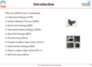
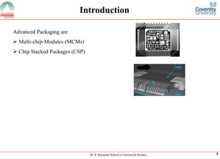
M. S. Ramaiah School of Advanced Studies 
1 
M. Sc. (Engg.) in Electronics System Design Engineering 
GREESHMA S 
CWB0913004 , FT-2013 
7thModule Presentation 
Module code : ESE2507 
Module name : Electronic Board Design 
Module leader: Mr. Ugra Mohan Roy 
Presentation on : 13/06/2014 
Packaging issues of optical component
M. S. Ramaiah School of Advanced Studies 
2 
•INTRODUCTION 
•PACKAGESERVESMULTIPLEFUNCTIONS 
•OPTICALPACKAGINGHIERARCHY 
•OPTICALPACKAGINGMATERIALS 
•EXAMPLE:WHYOPTICS? 
•ISSUESOFOPTICALPACKAGING 
•OPTICALPCBROADMAP 
•CONCLUSION 
•REFERENCES 
Overview
M. S. Ramaiah School of Advanced Studies 
3IntroductionThere are different types of packaging 
Chip Scale Packages (CSP) 
Surface Mounted Devices (SMD) 
Dual in-line Package (DIP) 
Thin Small Outline Package (TSOP) 
Quad Flat Package (QFP) 
Pin Grid Array (PGA) 
Ceramic Leadless Chip Carrier (CLCC) 
Small Outline Package (SOP) 
Plastic Leadless Chip Carrier (PLCC) 
Ball Grid Array (BGA)
M. S. Ramaiah School of Advanced Studies 
4 
Introduction 
Advanced Packaging are 
Multi-chip-Modules (MCMs) 
Chip Stacked Packages (CSP)
M. S. Ramaiah School of Advanced Studies 
5 
Package Serves Multiple Functions 
Protection –Environmental Management of Device 
Connectivity and routing –Electrical, Optical, Material–Including Power Management and Signal Integrity 
Mechanical Stress Control 
Thermal Management 
Testability and Burn-in
M. S. Ramaiah School of Advanced Studies 
6Optical Packaging Hierarchy
M. S. Ramaiah School of Advanced Studies 
7Optical Packaging Material
M. S. Ramaiah School of Advanced Studies 
8Example : Why Optics? Electrical Buses become increasingly difficult at high data rates (physics): • Increasing losses & cross-talk • Frequency resonant affects• Optical data transmission is easier: • Much lower loss, esp. at higher data rates• Additional advantages include: • Cable bulk, connector size, EMI… • Potential power savings 
•BW * Distance > electrical
M. S. Ramaiah School of Advanced Studies 
9Optical PCB technology has been researched for several years; however, significant issues remain before commercial implementation can be realized: 
•Waveguide fabrication at production scale 
•Optical PCB fabrication 
•Optical coupling (such as device-board and board-to-backplane) 
•Assembly 
•Optoelectronic devices in standard ”IC-like” packages used in optical PCB 
•Reliability (waveguide, connector, OE device, packaging materials, and system-level qualification) 
•Test vehicles… 
•Testing methods, equipments and applied standards
M. S. Ramaiah School of Advanced Studies 
10 
Issues of Optical Packaging
M. S. Ramaiah School of Advanced Studies 
11Optical PCB Roadmap
M. S. Ramaiah School of Advanced Studies 
12ConclusionLithium Niobateis the best optical packaging material. FEM analysis is used to measure Mechanical stress of the optical component. Optical packaging is better than Electrical Packaging. The challenges and solutions of integration of high performance waveguides on packages and PCBs have dealt.
M. S. Ramaiah School of Advanced Studies 
13Reference 
1.Henning Schröder(2011). Optical Packaging . Germany TechnischeUniversitätBerlin 625-632. 
2.YuzoIshii (2003). Fully SMT-Compatible Optical-I/O Package With MicrolensArray Interface. Japan JOURNAL OF LIGHTWAVE TECHNOLOGY 275-282.
M. S. Ramaiah School of Advanced Studies 
14Thank You

Packaging issues of optical component

  • 1.
    M. S. RamaiahSchool of Advanced Studies 1 M. Sc. (Engg.) in Electronics System Design Engineering GREESHMA S CWB0913004 , FT-2013 7thModule Presentation Module code : ESE2507 Module name : Electronic Board Design Module leader: Mr. Ugra Mohan Roy Presentation on : 13/06/2014 Packaging issues of optical component
  • 2.
    M. S. RamaiahSchool of Advanced Studies 2 •INTRODUCTION •PACKAGESERVESMULTIPLEFUNCTIONS •OPTICALPACKAGINGHIERARCHY •OPTICALPACKAGINGMATERIALS •EXAMPLE:WHYOPTICS? •ISSUESOFOPTICALPACKAGING •OPTICALPCBROADMAP •CONCLUSION •REFERENCES Overview
  • 3.
    M. S. RamaiahSchool of Advanced Studies 3IntroductionThere are different types of packaging Chip Scale Packages (CSP) Surface Mounted Devices (SMD) Dual in-line Package (DIP) Thin Small Outline Package (TSOP) Quad Flat Package (QFP) Pin Grid Array (PGA) Ceramic Leadless Chip Carrier (CLCC) Small Outline Package (SOP) Plastic Leadless Chip Carrier (PLCC) Ball Grid Array (BGA)
  • 4.
    M. S. RamaiahSchool of Advanced Studies 4 Introduction Advanced Packaging are Multi-chip-Modules (MCMs) Chip Stacked Packages (CSP)
  • 5.
    M. S. RamaiahSchool of Advanced Studies 5 Package Serves Multiple Functions Protection –Environmental Management of Device Connectivity and routing –Electrical, Optical, Material–Including Power Management and Signal Integrity Mechanical Stress Control Thermal Management Testability and Burn-in
  • 6.
    M. S. RamaiahSchool of Advanced Studies 6Optical Packaging Hierarchy
  • 7.
    M. S. RamaiahSchool of Advanced Studies 7Optical Packaging Material
  • 8.
    M. S. RamaiahSchool of Advanced Studies 8Example : Why Optics? Electrical Buses become increasingly difficult at high data rates (physics): • Increasing losses & cross-talk • Frequency resonant affects• Optical data transmission is easier: • Much lower loss, esp. at higher data rates• Additional advantages include: • Cable bulk, connector size, EMI… • Potential power savings •BW * Distance > electrical
  • 9.
    M. S. RamaiahSchool of Advanced Studies 9Optical PCB technology has been researched for several years; however, significant issues remain before commercial implementation can be realized: •Waveguide fabrication at production scale •Optical PCB fabrication •Optical coupling (such as device-board and board-to-backplane) •Assembly •Optoelectronic devices in standard ”IC-like” packages used in optical PCB •Reliability (waveguide, connector, OE device, packaging materials, and system-level qualification) •Test vehicles… •Testing methods, equipments and applied standards
  • 10.
    M. S. RamaiahSchool of Advanced Studies 10 Issues of Optical Packaging
  • 11.
    M. S. RamaiahSchool of Advanced Studies 11Optical PCB Roadmap
  • 12.
    M. S. RamaiahSchool of Advanced Studies 12ConclusionLithium Niobateis the best optical packaging material. FEM analysis is used to measure Mechanical stress of the optical component. Optical packaging is better than Electrical Packaging. The challenges and solutions of integration of high performance waveguides on packages and PCBs have dealt.
  • 13.
    M. S. RamaiahSchool of Advanced Studies 13Reference 1.Henning Schröder(2011). Optical Packaging . Germany TechnischeUniversitätBerlin 625-632. 2.YuzoIshii (2003). Fully SMT-Compatible Optical-I/O Package With MicrolensArray Interface. Japan JOURNAL OF LIGHTWAVE TECHNOLOGY 275-282.
  • 14.
    M. S. RamaiahSchool of Advanced Studies 14Thank You