The document describes a method for speeding up cycle-based logic simulation using graphics processing units (GPUs). The authors develop a parallel cycle-based logic simulation algorithm that uses and-inverter graphs (AIGs) as the design representation. They create two clustering algorithms that partition circuit gates into independent blocks that can be simulated concurrently. Experimental results show speedups of up to 5x using the first clustering algorithm and up to 21x using the second algorithm on several benchmarks. The work demonstrates that GPUs can significantly accelerate logic simulation through parallelization.
![Int J Parallel Prog
DOI 10.1007/s10766-011-0164-7
Speeding Up Cycle Based Logic Simulation Using
Graphics Processing Units
Alper Sen · Baris Aksanli · Murat Bozkurt
Received: 15 October 2010 / Accepted: 30 December 2010
© Springer Science+Business Media, LLC 2011
Abstract Verification has grown to dominate the cost of electronic system design,
consuming about 60% of design effort. Among several verification techniques, logic
simulation remains the major verification technique. Speeding up logic simulation
results in great savings and shorter time-to-market. We parallelize logic simulation
using Graphics Processing Units (GPUs). In the past, GPUs were special-purpose
application accelerators, suitable only for conventional graphics applications. The new
generations of GPU architecture provide easier programmability and increased gener-
ality while maintaining the tremendous memory bandwidth and computational power
of traditional GPUs. We develop a parallel cycle-based logic simulation algorithm that
uses And Inverter Graphs (AIGs) as design representations. AIGs have proven to be an
effective representation for various design automation applications, and we obtain sim-
ilar benefits for speeding up logic simulation. We develop two clustering algorithms
that partition the gates in the designs into independent blocks. Our algorithms exploit
the massively parallel GPU architecture featuring thousands of concurrent threads,
fast memory, and memory coalescing for optimizations. We demonstrate up-to 5x and
21x speedups on several benchmarks using our simulation system with the first and
second clustering algorithms, respectively. Our work ultimately results in significant
reduction in the overall design cycle.
Keywords Graphics processing units (GPU) · Parallel logic simulation ·
Cycle based simulation · And inverter graph (AIG)
This article is an extended version of a conference paper that appeared at ISPDC 2010 [27].
A. Sen (B · B. Aksanli · M. Bozkurt
)
Department of Computer Engineering, Bogazici University, 34342 Istanbul, Turkey
e-mail: alper.sen@boun.edu.tr
123](https://image.slidesharecdn.com/p5-verification-120220090041-phpapp01/85/P5-verification-1-320.jpg)
![Int J Parallel Prog
DOI 10.1007/s10766-011-0164-7
Speeding Up Cycle Based Logic Simulation Using
Graphics Processing Units
Alper Sen · Baris Aksanli · Murat Bozkurt
Received: 15 October 2010 / Accepted: 30 December 2010
© Springer Science+Business Media, LLC 2011
Abstract Verification has grown to dominate the cost of electronic system design,
consuming about 60% of design effort. Among several verification techniques, logic
simulation remains the major verification technique. Speeding up logic simulation
results in great savings and shorter time-to-market. We parallelize logic simulation
using Graphics Processing Units (GPUs). In the past, GPUs were special-purpose
application accelerators, suitable only for conventional graphics applications. The new
generations of GPU architecture provide easier programmability and increased gener-
ality while maintaining the tremendous memory bandwidth and computational power
of traditional GPUs. We develop a parallel cycle-based logic simulation algorithm that
uses And Inverter Graphs (AIGs) as design representations. AIGs have proven to be an
effective representation for various design automation applications, and we obtain sim-
ilar benefits for speeding up logic simulation. We develop two clustering algorithms
that partition the gates in the designs into independent blocks. Our algorithms exploit
the massively parallel GPU architecture featuring thousands of concurrent threads,
fast memory, and memory coalescing for optimizations. We demonstrate up-to 5x and
21x speedups on several benchmarks using our simulation system with the first and
second clustering algorithms, respectively. Our work ultimately results in significant
reduction in the overall design cycle.
Keywords Graphics processing units (GPU) · Parallel logic simulation ·
Cycle based simulation · And inverter graph (AIG)
This article is an extended version of a conference paper that appeared at ISPDC 2010 [27].
A. Sen (B · B. Aksanli · M. Bozkurt
)
Department of Computer Engineering, Bogazici University, 34342 Istanbul, Turkey
e-mail: alper.sen@boun.edu.tr
123](https://image.slidesharecdn.com/p5-verification-120220090041-phpapp01/75/P5-verification-1-2048.jpg)
![Int J Parallel Prog
1 Introduction
Complexity of electronic designs have been rapidly growing. Billions of transistors
are commonly placed in designs to generate higher performance. Multicore and many
core systems provide the performance by handling more work in parallel. However,
the complexity in electronic designs poses a great challenge for building such systems,
where designs continue to be released with latent bugs. Functional design verification
is the task of establishing that a given design accurately implements the intended
functional behavior (specification). Today, design verification has grown to dominate
the cost of electronic system design, in fact, consuming about 60% of design effort
[5]. Among several verification techniques, logic simulation remains to be the major
verification technique due to its applicability to real designs and its relative ease of
use. However, logic simulation of designs with millions of components is time con-
suming and has become a bottleneck in the design process. Any means to speedup
logic simulation results in productivity gains and faster time-to-market.
We observe that electronic designs exhibit a lot of parallelism that can be exploited
by parallel algorithms. In fact, there are parallel electronic design automation algo-
rithms for almost all stages in the implementation of an electronic design such as logic
optimization, floor-planning, routing, and physical verification stages. In this paper,
we focus on parallelization of logic simulation of electronic designs using Graphics
Processing Units (GPUs).
In the past, Graphics Processing Units (GPUs) were special-purpose application
accelerators, suitable only for conventional graphics applications. Nowadays, GPUs
are routinely used in applications other than graphics such as computational biol-
ogy, computational finance and electronic designs, where huge speedups have been
achieved [22]. This is a result of the availability of extremely high performance hard-
ware (for example, a GTX 480 GPU provides 1.35 Tflops with 480 cores and is under
$500), and the availability of general purpose programming models such as Com-
pute Unified Device Architecture (CUDA) by NVIDIA [13]. CUDA is an extension
to C language and is based on a few abstractions for parallel programming. CUDA
has accelerated the development of parallel applications beyond that of the original
purpose of graphics processing.
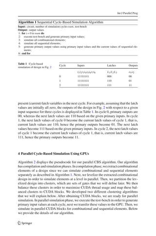
There are two main types of logic simulation; Cycle-Based Simulation (CBS) and
Event-Based Simulation (EBS). In CBS, the evaluation schedule of gates in the design
for each step of simulation is determined once at the compilation time of the simulator.
EBS has a more complicated scheduling policy where a gate is simulated only if at least
one of its input values have changed. Both CBS and EBS are commonly used in the
industry. In this paper, we work with CBS since it has a less complicated static sched-
uling policy that is amenable to better parallelization. However, we also note that logic
simulation has been classified as the most challenging Computer Aided Design pattern
to parallelize [7]. The ratio of communication (between gate and gate) to Boolean eval-
uation is high. Since the communication pattern of logic simulation often defy a pat-
tern, it is difficult to assign elements to processors so that communicating elements are
always close. High performance loss due to communication overhead is reported [26].
Logic simulation proceeds in two phases; compilation and simulation. The compi-
lation phase is part of any modern simulator and is required to convert the design into
123](https://image.slidesharecdn.com/p5-verification-120220090041-phpapp01/85/P5-verification-2-320.jpg)
![Int J Parallel Prog
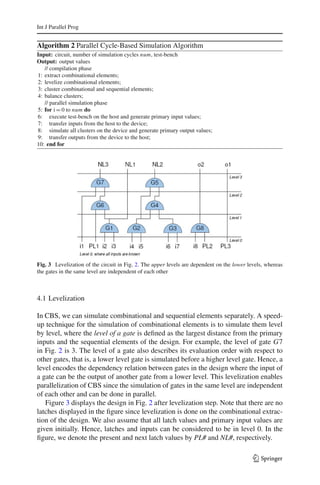
an appropriate form for the simulation phase. Our GPU based solution is also com-
posed of these two phases. In the compilation phase, we perform several operations
namely combinational logic extraction, levelization, clustering, and balancing opera-
tions. This phase has several GPU architecture dependent optimizations such as the
efficient usage of shared memory and memory coalescing. Levelization helps deter-
mine the dependency between gates, where gates in the same level can be simulated in
parallel. Clustering helps partition the design into a collection of smaller parts where
each part can be simulated independent of other parts. Balancing helps optimize the
usage of threads for a SIMD instruction. These operations are necessary because in
a gate level design, certain gates could have hundreds or thousands of fanouts while
most will have a few fanouts resulting in irregular data access patterns. Clustering
and balancing help organize access patterns for effective simulation. The simulation
phase is where thousands of threads are available to simulate the compiled design
in parallel. We use several optimizations in simulation phase in order to reduce the
communication overhead between the GPU and the CPU. In both phases, we exploit
the GPU memory resources as efficiently as possible in order to have low latency.
Our design representation for logic simulation is different from the other design
representations. We use And-Inverter Graphs (AIGs), in particular we use the AIGER
format [2]. AIG is an efficient representation for manipulation of boolean functions. It
is increasingly used in logic synthesis, technology mapping, verification, and boolean
satisfiability checking [6,10,20,21,28]. However, to the best of our knowledge, our
work is the first GPU based electronic design automation solution using AIGs. Since
we use AIGs with only a single type of combinational gate (and-gate), our algorithms
can efficiently use the limited low latency memory spaces provided by the GPU.
We developed two clustering algorithms. The first one clusters gates using a given
threshold, and the second one improves clustering with that of merging and balancing
steps and incorporates memory coalescing and efficient utilization of shared mem-
ory. We validated the effectiveness of our parallel CBS algorithm for both types of
clustering with several benchmarks from IWLS, and AIGER [2,17,24]. We compared
our parallel CBS algorithm with that of a sequential CBS algorithm. Our experiments
show that parallel CBS can speedup the simulation of designs over the sequential algo-
rithm. In particular, we obtained up-to 5x speedup with the first clustering algorithm
and up-to 21x with the second clustering algorithm. We obtain better speedups with
larger circuits.
This paper is organized as follows. In the next section, we give an overview of related
work in logic simulation and General Purpose computation on GPUs (GPGPU). We
then describe background in CUDA, AIG format and logic simulation in Sect. 3. In
Sect. 4, we describe our parallel CBS algorithm together with two clustering algo-
rithms and CUDA optimizations. Our experiments are in Sect. 6. Finally, conclusions
and future work are described.
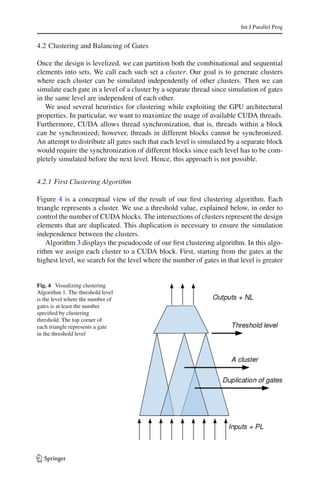
2 Related Work
Catanzaro et al. [7] explain design patterns for parallelization in Computer Aided
Design (CAD). The authors consider 17 different CAD algorithms and partition
123](https://image.slidesharecdn.com/p5-verification-120220090041-phpapp01/85/P5-verification-3-320.jpg)
![Int J Parallel Prog
these algorithms in three categories; graph algorithms, branch and bound search,
and linear algebra. They also state that graph algorithms in CAD (of which logic
simulation is a member) are the hardest to parallelize among these categories. Sim-
ilarly, CAD case studies of GPU acceleration can be found in [12]. Some of these
case studies are spice simulation, fault simulation, static timing analysis, boolean
satisfiability, fault dictionary computation, and power grid analysis. The authors
describe optimization techniques for irregular EDA applications on GPUs in [14].
In particular, they make use of memory coalescing and shared memory utiliza-
tions that improve the speedup of sparse matrix vector product and breadth first
search.
There has been a lot of work on parallel logic simulation using architectures other
than GPUs. There are several surveys on parallel logic simulation [4,19]. In particular,
cycle-based simulation approaches are used by IBM and others [15]. The simulation
algorithms in these works are aimed at loosely coupled processor systems.
Different partitioning algorithms for electronic designs are described in [3,18].
Some of these algorithms are based on performance, layout, clustering, network
flow, and spectral methods. Our partitioning approach is similar to cone clustering
described in [16], where a fanin cone of a circuit element embodies an area of com-
binational logic that has the potential to influence signal values provided by that
element.
Several general purpose GPU applications can be found in [13,22]. The application
domain ranges from physics to finance and the medical field. The work in [11] gives a
performance study of general purpose applications using CUDA and compares them
with that of applications written using OpenMP.
There is another general purpose programming environment for GPUs named
OpenCL. OpenCL [23] is a relatively new standard that is very similar to CUDA in
that it is also an extension of C language. CUDA is specific to NVIDIA GPUs, whereas
OpenCL can be run on different architectures and gives you portability at the expense
of potentially sub-optimal performance for any specific platform. Also, CUDA is a
more mature environment with high-performance libraries and accompanying tools
like debuggers and profilers.
Our CBS algorithm is most similar to the work by Chatterjee et al. [9]. However,
there are several differences. We use AIGs as gate level representation whereas they
support a generic library of gates. AIGs allow us to efficiently use the limited low
latency memory spaces. We use a threshold value in our first clustering algorithm,
whereas they start clusters from the primary outputs. We fix the number of blocks
in our second clustering algorithm in order to maximize parallel thread execution.
We encode variables in order to better utilize shared memory and we explicitly use
memory coalescing, whereas these are not used in [9].
There is an earlier logic simulation algorithm using GPUs by Perinkulam [25].
However, this algorithm does not provide performance benefits since they do not opti-
mize data transfer between GPU and CPU, use a different partitioning approach, and
do not use the general purpose programming language CUDA. There is also a recent
work on event-based simulation algorithm, which is also a commonly used simulation
technique in the industry, using CUDA [8].
123](https://image.slidesharecdn.com/p5-verification-120220090041-phpapp01/85/P5-verification-4-320.jpg)
![Int J Parallel Prog
3 Background
In this section, we are going to present background on CUDA programming, AIGs,
and sequential cycle based logic simulation of electronic designs.
3.1 CUDA Programming
Compute Unified Device Architecture (CUDA) is a small C library extension devel-
oped by NVIDIA to expose the computational horsepower of NVIDIA GPUs [13].
GPU is a compute device that serves as a co-processor for the host CPU. CUDA
can be considered as an instance of widely used Single Program Multiple Data
(SPMD) parallel programming models. A CUDA program supplies a single source
code encompassing both host and device code. Execution of this code consists of
one or more phases that are executed either on the host or device. The phases that
exhibit little amount of parallelism are executed on the host and rich amount of
parallelism are executed on the device. The device code is referred to as kernel
code.
The smallest execution units in CUDA are threads. Thousands of threads can work
concurrently at a time. GPU has its own device memory and provides different types
of memory spaces available to threads during their execution. Each thread has a private
local memory in addition to the registers allocated to it. A group of threads forms a
CUDA block. A CUDA block can have at most 512 threads, where each thread has
a unique id. A group of blocks forms a CUDA grid. Each thread block has a shared
memory visible to all threads of the block within the lifetime of the block. Access to
shared memory is fast like that of a register. Threads in the same block can synchro-
nize using a barrier, whereas threads from different blocks can not synchronize. Each
thread has access to the global device memory throughout the application. Access to
the global memory is slow and around 400–600 cycles. There are also special memory
spaces such as texture, constant, and page-locked (pinned) memories. All types of
memory spaces are limited in size, and should therefore be handled carefully in the
program.
Figure 1 displays general NVIDIA CUDA architecture with N streaming mul-
tiprocessors composed of M streaming processors. For an NVIDIA FX3800 GPU,
N = 24 and M = 8. Each multiprocessor can execute 768 threads in parallel and
shared memory size is limited where each multiprocessor can have 16 KB of shared
memory.
3.2 And-Inverter Graph (AIG)
And-Inverter Graph (AIG) is a directed, acyclic graph that represents a structural
implementation of the logical functionality of a design or circuit. AIGER format is an
implementation of AIGs [2]. An AIG is composed of two-input and-nodes (combi-
national elements) representing logical conjunction, single input nodes representing
memory elements (latches, sequential elements), nodes labeled with variable names
123](https://image.slidesharecdn.com/p5-verification-120220090041-phpapp01/85/P5-verification-5-320.jpg)
![Int J Parallel Prog
Fig. 1 CUDA hardware and memory architecture (Source: NVIDIA CUDA programming Guide [13])
representing inputs and outputs, and edges optionally containing markers indicating
logical negation. We refer to and-nodes and latches as gates. AIG is an efficient rep-
resentation for manipulation of boolean functions.
The combinational logic of an arbitrary Boolean network can be factored and
transformed into an AIG using DeMorgans rule. The following properties of
AIGs facilitate development of robust applications in synthesis, mapping, and
formal verification. Structural hashing ensures that AIGs do not contain struc-
turally identical nodes. Inverters are represented as edge attributes. As a result,
single-input nodes representing inverters and buffers do not have to be created.
This saves memory and allows for applying DeMorgans rule on-the-fly, which
increases logic sharing. The AIG representation is uniform and fine-grain, result-
ing in a small, fixed amount of memory per node. The nodes are stored in
one memory array in a topological order, resulting in fast, CPU-cache-friendly
traversals.
There has been a growing interest in AIGs as a functional representation for a
variety of tasks in Electronic Design Automation (EDA) such as logic synthesis,
technology mapping, verification, and equivalence checking [6,10,20,21,28]. Espe-
cially, the recent emergence of efficient boolean satisfiability (SAT) solvers that use
AIGs instead of the Binary Decision Diagrams (BDD) has made AIGs popular in
EDA. A tool called ABC [6] features an AIG package, several AIG-based synthe-
sis and equivalence-checking techniques, as well as an implementation of sequential
synthesis.
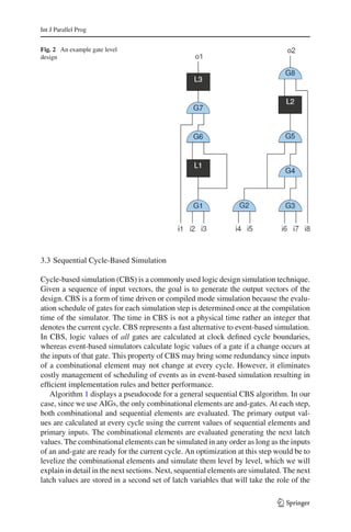
Figure 2 displays an example gate level design. In this figure, and-gates are iden-
tified as G#, where # stands for the unique gate number; and latches are identified as
L#, where # stands for the unique latch number. i# and o# stand for (primary) inputs
and (primary) outputs, respectively.
123](https://image.slidesharecdn.com/p5-verification-120220090041-phpapp01/85/P5-verification-6-320.jpg)
![Int J Parallel Prog
4.2.2 Second Clustering Algorithm
In this algorithm, we build clusters starting from the primary outputs and latches
instead of starting from the user given threshold level as in the first clustering algo-
rithm (Fig. 6). This allows us not to have any remaining gates as was the case above.
Also, since designs can have varying number of outputs and latches, the number of
clusters and the sizes of clusters can vary. This necessitates further steps to optimize
thread usage. For this purpose, we develop new steps for merging and balancing of
clusters. This avoids assigning every cluster to a CUDA block as in the previous algo-
rithm, rather we reshape clusters into an optimized format then assign those clusters
to CUDA blocks.
Algorithm 4 shows our second clustering algorithm. We next describe the steps in
the algorithm in greater detail.
– Step 1. Obtain clusters In this algorithm we do not assign each cluster to a CUDA
block as was done in the previous clustering algorithm. Rather, our goal is to build
many clusters starting from primary outputs and latches. We add the cone of logic
of both primary outputs and latches and form clusters, named cluster O L. How-
ever, when going back from a gate, we stop at the latches. At the end of this step, the
number of clusters is the sum of the number of primary outputs and the number of
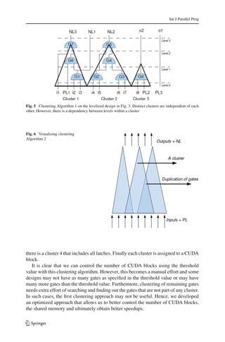
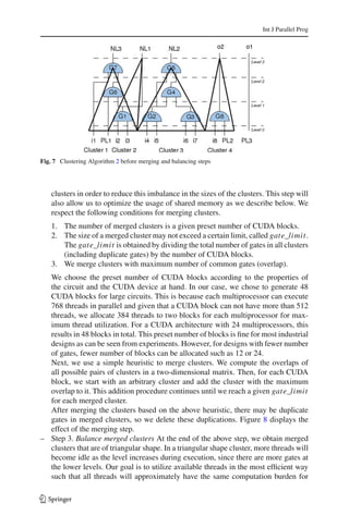
latches. Figure 7 displays application of this step on the levelized design in Fig. 3.
– Step 2. Merge clusters After the above step is completed, there may be clusters
with an imbalance in distribution of gates to clusters. Hence, we need to merge
Algorithm 4 Pseudocode for Second Clustering Algorithm
Input: levelized circuit, number of CUDA blocks num Blocks
Output: merged and balanced cluster of gates
// Step 1. obtain clusters
1: for each primary output or latch O L do
2: add the cone of logic for O L to cluster O L;
3: end for
// Step 2. merge clusters
4: gate_limit = total number of gates in all cluster O L/number of blocks;
5: compute overlaps of all possible pairs of clusters;
6: for i = 1 to num Blocks do
7: let clusterC L be an arbitrary unmarked cluster and mergedC L[i] = ∅;
8: mergedC L[i] = mergedC L[i] ∪ clusterC L;
9: mark clusterC L;
10: repeat
11: clusterC Li = an unmarked cluster with maximum overlap with clusterC L;
12: mergedC L[i] = mergedC L[i] ∪ clusterC Li;
13: mark clusterC Li;
14: until number of gates in mergedC L[i] reaches gate_limit;
15: delete duplicate gates in each mergedC L[i];
16: end for
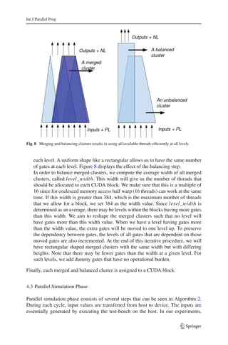
// Step 3. balance merged clusters
17: level_width = average width of all merged clusters;
18: for each merged cluster mergedC L[i] do
19: move gates in mergedC L[i] such that the cluster has a level_width wide rectangular shape;
20: end for
123](https://image.slidesharecdn.com/p5-verification-120220090041-phpapp01/85/P5-verification-13-320.jpg)
![Int J Parallel Prog
Algorithm 5 Parallel Block Simulation Kernel Pseudocode
1: _ _global_ _ void simulationKernel(...){
2:
3: _ _shared_ _ unsigned char vars[8000]; // keep encoded intermediate values
4: numberOfThreads = blockDim.x;
5: index = threadIdx.x; start = blockIdx.x * numberofThreads;
6: vars = coalesced read of encoded values from global device memory;
7: for i = 0; i < level; i + + do
8: // coalesced read gate variables from global device memory
9: i1 = firstInput[start+index];
10: i2 = secondInput[start+index];
11: o = output[start+index];
12: decode variable i1 as v1, i2 as v2;
13: val = v1 ∧ v2;
14: write encoded val to vars array;
15: index+ = number O f T hr eads;
16: _ _syncthreads();
17: end for
18: coalesced write vars to global device memory;
19: }
we mainly used random test-benches, hence the input generation could be optimized
as described in the next section. Once the inputs are ready, all CUDA blocks can
be executed by executing a kernel function. An execution of a block with combina-
tional elements proceeds level by level and after each level is simulated the threads
of the block synchronize using a barrier. This process continues until all levels are
completed. We used coalesced memory access for reading and writing gate variables
between the global memory and the CUDA processors. We increased the number of
gates that can be efficiently simulated in a block by encoding the intermediate gate
outputs and storing these in the shared memory. Also, the intermediate gate output
values are stored in shared memory in an encoded fashion, which we describe in next
section. At the beginning of a cycle, blocks fetch relevant design data (gate variables)
and input values from device memory in a coalesced manner. At the end of the cycle,
output and latch values are transferred from device to host. In particular, we stored
the design structure, primary inputs, primary outputs and latches in the device mem-
ory and frequently accessed data structures such as intermediate and-gate values of
a block in the shared memory. Our particular simulation kernel function is shown in
Algorithm 5. We next describe our CUDA optimizations in more detail.
5 CUDA Optimizations
We applied several optimization methods to increase performance of our algorithms.
To develop an effective CUDA program, one needs to have knowledge of the GPU
architecture such as shared memory, memory coalescing and memory transfer over-
head. Communication overhead is a major cost, so we exploited CUDA’s faster shared
memory, register and pinned memories in our implementation.
In CUDA, one can allocate memory space in host memory dynamically by using
Cuda MallocH ost function instead of the ordinary C malloc function. This uses
123](https://image.slidesharecdn.com/p5-verification-120220090041-phpapp01/85/P5-verification-16-320.jpg)
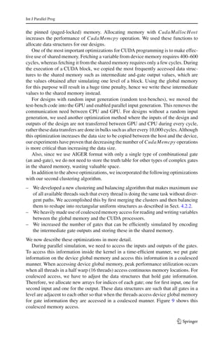
![Int J Parallel Prog
Fig. 9 Coalesced memory access
Above we described how we used shared memory for fast access. However, shared
memory size is limited. Each multiprocessor can have 16 KB of shared memory, when
we use 2 blocks for each multiprocessor then each will have 8 KB of shared memory.
If we use one char variable for each gate output value, we can have at most 8,000
variables for a block (8 KB max shared memory for a block), and therefore the total
number of variables in a design can be at most 48 blocks * 8,000 variables = 384,000
variables. This number may be small for large designs. Therefore, we developed an
efficient representation to keep gate output values by using 1 unsigned char variable
(8 bits) for 8 gate outputs since a gate output can only be 0 or 1. At the start of each
block simulation, we bring these encoded variables from device global memory in
a coalesced manner as well. With this representation, we can have 64,000 variables
for a block and in total 48 blocks * 64,000 variables = 3,072,000 variables. This is
equal to the sum of the number of and-gates, latches, primary inputs and outputs in
a design. If we assumed that there is a 30% duplication of gates among blocks, then
we can simulate designs with up to 2 million gates approximately. Similarly encoded
variables are read and written in a coalesced manner.
6 Experimental Results
We validated the effectiveness of our two GPU based parallel CBS algorithms on
several test cases. We used test cases from IWLS [17], OpenCores [24] and AIGER
[2]. These test cases include ldpc-encoder (low density parity check encoder), des-perf
(triple DES optimized for performance), wb-conmax (wishbone conmax IP core), aes-
core (AES Encryption/Decryption IP Core) pci-bridge32, ethernet, vga-lcd (wishbone
compliant enhanced vga/lcd controller), and several other designs. These test cases
either had their own test benches or we generated random test benches for them.
Table 2 displays the list of test cases that we used in our experiments and their design
characteristics including the number of levels and the number of CUDA blocks used
for their simulation for both clustering algorithms. For some test cases, we generated
AIGER format of designs using ABC tool [1].
We performed our experiments on an Intel Xeon CPU with two 2.27 GHz multi-
processors, 32GB of memory and a CUDA–enabled NVIDIA Quadro FX3800 GPU
with 1 GB device memory and 24 streaming multiprocessors each with 8 streaming
processors.
123](https://image.slidesharecdn.com/p5-verification-120220090041-phpapp01/85/P5-verification-18-320.jpg)
![Int J Parallel Prog
Table 2 Experimental test cases
Design Vars Inputs Latches Outputs And-Gates Levels Blocks1 Blocks2
ldpc-encoder 220,684 1,723 0 2,048 218,961 19 288 48
vga-lcd 143,879 89 17,079 109 126,711 23 145 48
des-perf 100,500 17,850 0 9,038 82,650 19 373 48
ethernet 80,326 98 10,544 115 69,684 31 364 48
wb-conmax 49,753 1,130 770 1,416 47,853 26 261 24
tv80 7,665 14 359 32 7,292 39 34 24
aes-core 22,841 1,319 0 668 21,522 25 126 24
ac97-ctrl 12,624 84 2,199 48 10,341 8 495 24
pci-bridge32 26,305 162 3,359 207 22,784 29 146 24
system-cdes 2,813 132 190 65 2,491 22 48 24
pci-spoci-ctrl 880 25 60 13 795 14 29 24
sasc 740 16 117 12 607 7 49 24
Table 3 Experimental results for 100,000 cycles
Design SEQ(sec) PAR1(sec) PAR2(sec) Speedup1 Speedup2
ldpc-encoder 382.21 74.79 24.32 5.11 15.72
vga-lcd 223.15 45.91 25.45 4.86 8.77
des-perf 180.62 65.68 8.53 2.75 21.17
ethernet 155.51 52.89 14.96 2.94 10.40
wb-conmax 94.81 33.96 10.8 2.79 8.78
tv80 92.59 23.31 10.63 3.97 8.71
aes-core 83.64 35.63 7.97 2.35 10.49
ac97-ctrl 58.66 18.87 4.74 3.11 12.38
pci-bridge32 50.12 21.7 9.39 2.31 5.34
system-cdes 30.44 11.55 6.92 2.64 4.40
pci-spoci-ctrl 7.04 10.44 5.13 0.67 1.37
sasc 6.26 6.34 3.75 0.99 1.6
In Table 3, we demonstrate our experimental results. Column S E Q denotes the
results for sequential simulation using the default simulator that is available with AI-
GER [2]. Columns P A R1 and P A R2 denote the results for our parallel simulation
algorithms using the first and the second clustering algorithms, respectively. Col-
umns Speedup1 and Speedup2 denote the speedup of parallel algorithms over the
sequential algorithm. The times do not include the compilation phase in both cases but
include the time required to transfer the data between the GPU and the CPU. Figure 10
graphically displays the speedups.
We simulated the designs for different number of cycles ranging from 100, 500 K to
1 M. Figure 11 shows that the speedups are similar for different number of cycles for
123](https://image.slidesharecdn.com/p5-verification-120220090041-phpapp01/85/P5-verification-19-320.jpg)