Original Power MOSFET IRFP460PBF IRFP460 460 500V 20A TO-247 New Vishay Silic...AUTHELECTRONIC
Original Power MOSFET IRFP460PBF IRFP460 460 500V 20A TO-247 New Vishay Siliconix
https://authelectronic.com/original-power-mosfet-irfp460pbf-irfp460-460-500v-20a-to-247-new-vishay-siliconix
Original P-CHANNEL POWER MOSFETS IRFP9240PBF IRFP9240 9240 200V 12A TO-247 NewAUTHELECTRONIC
Original P-CHANNEL POWER MOSFETS IRFP9240PBF IRFP9240 9240 200V 12A TO-247 New
https://authelectronic.com/original-p-channel-power-mosfets-irfp9240pbf-irfp9240-9240-200v-12a-to-247-new
Original Power MOSFET IRFP240 IRFP240PBF 240 200V 20A TO-247 New Vishay Silic...AUTHELECTRONIC
Original Power MOSFET IRFP240 IRFP240PBF 240 200V 20A TO-247 New Vishay Siliconix
https://authelectronic.com/original-power-mosfet-irfp240-irfp240pbf-240-200v-20a-to-247-new-vishay-siliconix
Original N-Channel Mosfet IRFUC20PBF 600V 2A TO-251 New VishayAUTHELECTRONIC
Original N-Channel Mosfet IRFUC20PBF 600V 2A TO-251 New Vishay
https://authelectronic.com/original-n-channel-mosfet-irfuc20pbf-600v-2a-to-251-new-vishay
Original P-CHANNEL MOSFET IRF5210PBF IRF5210 5210 100V 38A TO-220 New IRAUTHELECTRONIC
Original P-CHANNEL MOSFET IRF5210PBF IRF5210 5210 100V 38A TO-220 New IR
https://authelectronic.com/original-p-channel-mosfet-irf5210pbf-irf5210-5210-100v-38a-to-220-new-ir
Original N Channel Mosfet IRF3710PBF IRF3710 3710 37A 100V NewAUTHELECTRONIC
Original N Channel Mosfet IRF3710PBF IRF3710 3710 37A 100V New
https://authelectronic.com/original-n-channel-mosfet-irf3710pbf-irf3710-3710-37a-100v-new
Original Power MOSFET IRFBF30 IRFBF30PBF 900V 3.6A New Vishay SiliconixAUTHELECTRONIC
Original Power MOSFET IRFBF30 IRFBF30PBF 900V 3.6A New Vishay Siliconix
https://authelectronic.com/original-power-mosfet-irfbf30-irfbf30pbf-900v-3-6a-new-vishay-siliconix
Original Mosfet N FDPF8N50NZ 8N50 8N50NZ 10V 4A TO-220 New FairchildAUTHELECTRONIC
Original Mosfet N FDPF8N50NZ 8N50 8N50NZ 10V 4A TO-220 New Fairchild
https://authelectronic.com/original-mosfet-n-fdpf8n50nz-8n50-8n50nz-10v-4a-to-220-new
Original N-Channel Power MOSFET IRF1010EPBF IRF1010 1010 60V 84A TO-220 New I...AUTHELECTRONIC
Original N-Channel Power MOSFET IRF1010EPBF IRF1010 1010 60V 84A TO-220 New International Rectifier
https://authelectronic.com/original-n-channel-power-mosfet-irf1010epbf-irf1010-1010-60v-84a-to-220-new-international-rectifier
Original N-channel 650 V 0.230 Ohm 12 A MDmesh V Power MOSFET in DPAK DPAK ST...AUTHELECTRONIC
Original N-channel 650 V 0.230 Ohm 12 A MDmesh V Power MOSFET in DPAK DPAK STF16N65M5 16N65M5 16N65 710V 12A TO-220FP New STMicroelectronics
https://authelectronic.com/original-n-channel-650-v-0-230-ohm-12-a-mdmesh-v-power-mosfet-in-dpak-dpak-stf16n65m5-16n65m5-16n65-710v-12a-to-220fp-new-stmicroelectronics
Sachpazis:Terzaghi Bearing Capacity Estimation in simple terms with Calculati...Dr.Costas Sachpazis
Terzaghi's soil bearing capacity theory, developed by Karl Terzaghi, is a fundamental principle in geotechnical engineering used to determine the bearing capacity of shallow foundations. This theory provides a method to calculate the ultimate bearing capacity of soil, which is the maximum load per unit area that the soil can support without undergoing shear failure. The Calculation HTML Code included.
Hierarchical Digital Twin of a Naval Power SystemKerry Sado
A hierarchical digital twin of a Naval DC power system has been developed and experimentally verified. Similar to other state-of-the-art digital twins, this technology creates a digital replica of the physical system executed in real-time or faster, which can modify hardware controls. However, its advantage stems from distributing computational efforts by utilizing a hierarchical structure composed of lower-level digital twin blocks and a higher-level system digital twin. Each digital twin block is associated with a physical subsystem of the hardware and communicates with a singular system digital twin, which creates a system-level response. By extracting information from each level of the hierarchy, power system controls of the hardware were reconfigured autonomously. This hierarchical digital twin development offers several advantages over other digital twins, particularly in the field of naval power systems. The hierarchical structure allows for greater computational efficiency and scalability while the ability to autonomously reconfigure hardware controls offers increased flexibility and responsiveness. The hierarchical decomposition and models utilized were well aligned with the physical twin, as indicated by the maximum deviations between the developed digital twin hierarchy and the hardware.
Welcome to WIPAC Monthly the magazine brought to you by the LinkedIn Group Water Industry Process Automation & Control.
In this month's edition, along with this month's industry news to celebrate the 13 years since the group was created we have articles including
A case study of the used of Advanced Process Control at the Wastewater Treatment works at Lleida in Spain
A look back on an article on smart wastewater networks in order to see how the industry has measured up in the interim around the adoption of Digital Transformation in the Water Industry.
Immunizing Image Classifiers Against Localized Adversary Attacksgerogepatton
This paper addresses the vulnerability of deep learning models, particularly convolutional neural networks
(CNN)s, to adversarial attacks and presents a proactive training technique designed to counter them. We
introduce a novel volumization algorithm, which transforms 2D images into 3D volumetric representations.
When combined with 3D convolution and deep curriculum learning optimization (CLO), itsignificantly improves
the immunity of models against localized universal attacks by up to 40%. We evaluate our proposed approach
using contemporary CNN architectures and the modified Canadian Institute for Advanced Research (CIFAR-10
and CIFAR-100) and ImageNet Large Scale Visual Recognition Challenge (ILSVRC12) datasets, showcasing
accuracy improvements over previous techniques. The results indicate that the combination of the volumetric
input and curriculum learning holds significant promise for mitigating adversarial attacks without necessitating
adversary training.
Hybrid optimization of pumped hydro system and solar- Engr. Abdul-Azeez.pdffxintegritypublishin
Advancements in technology unveil a myriad of electrical and electronic breakthroughs geared towards efficiently harnessing limited resources to meet human energy demands. The optimization of hybrid solar PV panels and pumped hydro energy supply systems plays a pivotal role in utilizing natural resources effectively. This initiative not only benefits humanity but also fosters environmental sustainability. The study investigated the design optimization of these hybrid systems, focusing on understanding solar radiation patterns, identifying geographical influences on solar radiation, formulating a mathematical model for system optimization, and determining the optimal configuration of PV panels and pumped hydro storage. Through a comparative analysis approach and eight weeks of data collection, the study addressed key research questions related to solar radiation patterns and optimal system design. The findings highlighted regions with heightened solar radiation levels, showcasing substantial potential for power generation and emphasizing the system's efficiency. Optimizing system design significantly boosted power generation, promoted renewable energy utilization, and enhanced energy storage capacity. The study underscored the benefits of optimizing hybrid solar PV panels and pumped hydro energy supply systems for sustainable energy usage. Optimizing the design of solar PV panels and pumped hydro energy supply systems as examined across diverse climatic conditions in a developing country, not only enhances power generation but also improves the integration of renewable energy sources and boosts energy storage capacities, particularly beneficial for less economically prosperous regions. Additionally, the study provides valuable insights for advancing energy research in economically viable areas. Recommendations included conducting site-specific assessments, utilizing advanced modeling tools, implementing regular maintenance protocols, and enhancing communication among system components.
NO1 Uk best vashikaran specialist in delhi vashikaran baba near me online vas...Amil Baba Dawood bangali
Contact with Dawood Bhai Just call on +92322-6382012 and we'll help you. We'll solve all your problems within 12 to 24 hours and with 101% guarantee and with astrology systematic. If you want to take any personal or professional advice then also you can call us on +92322-6382012 , ONLINE LOVE PROBLEM & Other all types of Daily Life Problem's.Then CALL or WHATSAPP us on +92322-6382012 and Get all these problems solutions here by Amil Baba DAWOOD BANGALI
#vashikaranspecialist #astrologer #palmistry #amliyaat #taweez #manpasandshadi #horoscope #spiritual #lovelife #lovespell #marriagespell#aamilbabainpakistan #amilbabainkarachi #powerfullblackmagicspell #kalajadumantarspecialist #realamilbaba #AmilbabainPakistan #astrologerincanada #astrologerindubai #lovespellsmaster #kalajaduspecialist #lovespellsthatwork #aamilbabainlahore#blackmagicformarriage #aamilbaba #kalajadu #kalailam #taweez #wazifaexpert #jadumantar #vashikaranspecialist #astrologer #palmistry #amliyaat #taweez #manpasandshadi #horoscope #spiritual #lovelife #lovespell #marriagespell#aamilbabainpakistan #amilbabainkarachi #powerfullblackmagicspell #kalajadumantarspecialist #realamilbaba #AmilbabainPakistan #astrologerincanada #astrologerindubai #lovespellsmaster #kalajaduspecialist #lovespellsthatwork #aamilbabainlahore #blackmagicforlove #blackmagicformarriage #aamilbaba #kalajadu #kalailam #taweez #wazifaexpert #jadumantar #vashikaranspecialist #astrologer #palmistry #amliyaat #taweez #manpasandshadi #horoscope #spiritual #lovelife #lovespell #marriagespell#aamilbabainpakistan #amilbabainkarachi #powerfullblackmagicspell #kalajadumantarspecialist #realamilbaba #AmilbabainPakistan #astrologerincanada #astrologerindubai #lovespellsmaster #kalajaduspecialist #lovespellsthatwork #aamilbabainlahore #Amilbabainuk #amilbabainspain #amilbabaindubai #Amilbabainnorway #amilbabainkrachi #amilbabainlahore #amilbabaingujranwalan #amilbabainislamabad
Governing Equations for Fundamental Aerodynamics_Anderson2010.pdf
Original Mosfet N-CHANNEL IRF840 TO-220 500V 8A New
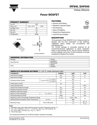
1. Document Number: 91070 www.vishay.com
S-81290-Rev. B, 16-Jun-08 1
Power MOSFET
IRF840, SiHF840
Vishay Siliconix
FEATURES
• Dynamic dV/dt Rating
• Repetitive Avalanche Rated
• Fast Switching
• Ease of Paralleling
• Simple Drive Requirements
• Lead (Pb)-free Available
DESCRIPTION
Third generation Power MOSFETs from Vishay provide the
designer with the best combination of fast switching,
ruggedized device design, low on-resistance and
cost-effectiveness.
The TO-220 package is universally preferred for all
commercial-industrial applications at power dissipation
levels to approximately 50 W. The low thermal resistance
and low package cost of the TO-220 contribute to its wide
acceptance throughout the industry.
Notes
a. Repetitive rating; pulse width limited by maximum junction temperature (see fig. 11).
b. VDD = 50 V, starting TJ = 25 °C, L = 14 mH, RG = 25 Ω, IAS = 8.0 A (see fig. 12).
c. ISD ≤ 8.0 A, dI/dt ≤ 100 A/µs, VDD ≤ VDS, TJ ≤ 150 °C.
d. 1.6 mm from case.
PRODUCT SUMMARY
VDS (V) 500
RDS(on) (Ω) VGS = 10 V 0.85
Qg (Max.) (nC) 63
Qgs (nC) 9.3
Qgd (nC) 32
Configuration Single
N-Channel MOSFET
G
D
S
TO-220
G
D
S
Available
RoHS*
COMPLIANT
ORDERING INFORMATION
Package TO-220
Lead (Pb)-free
IRF840PbF
SiHF840-E3
SnPb
IRF840
SiHF840
ABSOLUTE MAXIMUM RATINGS TC = 25 °C, unless otherwise noted
PARAMETER SYMBOL LIMIT UNIT
Drain-Source Voltage VDS 500 V
Gate-Source Voltage VGS ± 20 V
Continuous Drain Current VGS at 10 V
TC = 25 °C
ID
8.0
ATC = 100 °C 5.1
Pulsed Drain Currenta IDM 32
Linear Derating Factor 1.0 W/°C
Single Pulse Avalanche Energyb EAS 510 mJ
Repetitive Avalanche Currenta IAR 8.0 A
Repetitive Avalanche Energya EAR 13 mJ
Maximum Power Dissipation TC = 25 °C PD 125 W
Peak Diode Recovery dV/dtc dV/dt 3.5 V/ns
Operating Junction and Storage Temperature Range TJ, Tstg - 55 to + 150
°C
Soldering Recommendations (Peak Temperature) for 10 s 300d
Mounting Torque 6-32 or M3 screw
10 lbf · in
1.1 N · m
* Pb containing terminations are not RoHS compliant, exemptions may apply
2. www.vishay.com Document Number: 91070
2 S-81290-Rev. B, 16-Jun-08
IRF840, SiHF840
Vishay Siliconix
Notes
a. Repetitive rating; pulse width limited by maximum junction temperature (see fig. 11).
b. Pulse width ≤ 300 µs; duty cycle ≤ 2 %.
THERMAL RESISTANCE RATINGS
PARAMETER SYMBOL TYP. MAX. UNIT
Maximum Junction-to-Ambient RthJA - 62
°C/WCase-to-Sink, Flat, Greased Surface RthCS 0.50 -
Maximum Junction-to-Case (Drain) RthJC - 1.0
SPECIFICATIONS TJ = 25 °C, unless otherwise noted
PARAMETER SYMBOL TEST CONDITIONS MIN. TYP. MAX. UNIT
Static
Drain-Source Breakdown Voltage VDS VGS = 0 V, ID = 250 µA 500 - - V
VDS Temperature Coefficient ΔVDS/TJ Reference to 25 °C, ID = 1 mA - 0.78 - V/°C
Gate-Source Threshold Voltage VGS(th) VDS = VGS, ID = 250 µA 2.0 - 4.0 V
Gate-Source Leakage IGSS VGS = ± 20 V - - ± 100 nA
Zero Gate Voltage Drain Current IDSS
VDS = 500 V, VGS = 0 V - - 25
µA
VDS = 400 V, VGS = 0 V, TJ = 125 °C - - 250
Drain-Source On-State Resistance RDS(on) VGS = 10 V ID = 4.8 Ab - - 0.85 Ω
Forward Transconductance gfs VDS = 50 V, ID = 4.8 Ab 4.9 - - S
Dynamic
Input Capacitance Ciss VGS = 0 V,
VDS = 25 V,
f = 1.0 MHz, see fig. 5
- 1300 -
pFOutput Capacitance Coss - 310 -
Reverse Transfer Capacitance Crss - 120 -
Total Gate Charge Qg
VGS = 10 V
ID = 8 A, VDS = 400 V,
see fig. 6 and 13b
- - 63
nCGate-Source Charge Qgs - - 9.3
Gate-Drain Charge Qgd - - 32
Turn-On Delay Time td(on)
VDD = 250 V, ID = 8 A
RG = 9.1 Ω, RD = 31 Ω, see fig. 10b
- 14 -
ns
Rise Time tr - 23 -
Turn-Off Delay Time td(off) - 49 -
Fall Time tf - 20 -
Internal Drain Inductance LD
Between lead,
6 mm (0.25") from
package and center of
die contact
- 4.5 -
nH
Internal Source Inductance LS - 7.5 -
Drain-Source Body Diode Characteristics
Continuous Source-Drain Diode Current IS
MOSFET symbol
showing the
integral reverse
p - n junction diode
- - 8.0
A
Pulsed Diode Forward Currenta ISM - - 32
Body Diode Voltage VSD TJ = 25 °C, IS = 8 A, VGS = 0 Vb - - 2.0 V
Body Diode Reverse Recovery Time trr
TJ = 25 °C, IF = 8 A, dI/dt = 100 A/µsb
- 460 970 ns
Body Diode Reverse Recovery Charge Qrr - 4.2 8.9 µC
Forward Turn-On Time ton Intrinsic turn-on time is negligible (turn-on is dominated by LS and LD)
D
S
G
S
D
G
3. Document Number: 91070 www.vishay.com
S-81290-Rev. B, 16-Jun-08 3
IRF840, SiHF840
Vishay Siliconix
TYPICAL CHARACTERISTICS 25 °C, unless otherwise noted
Fig. 1 - Typical Output Characteristics, TC = 25 °C
Fig. 2 - Typical Output Characteristics, TC = 150 °C
Fig. 3 - Typical Transfer Characteristics
Fig. 4 - Normalized On-Resistance vs. Temperature
91070_01 VDS, Drain-to-Source Voltage (V)
ID,DrainCurrent(A)
101
100
100 101
Bottom
Top
VGS
15 V
10 V
8.0 V
7.0 V
6.0 V
5.5 V
5.0 V
4.5 V
20 µs Pulse Width
TC = 25 °C
4.5 V
91070_02
101
100
100 101
ID,DrainCurrent(A)
4.5 V
Bottom
Top
VGS
15 V
10 V
8.0 V
7.0 V
6.0 V
5.5 V
5.0 V
4.5 V
20 µs Pulse Width
TC = 150 °C
VDS, Drain-to-Source Voltage (V)
91070_03
25 °C
150 °C
20 µs Pulse Width
VDS = 50 V
101
100
ID,DrainCurrent(A)
VGS, Gate-to-Source Voltage (V)
5 6 7 8 9 104
91070_04
3.0
0.0
0.5
1.0
1.5
2.0
2.5
- 60 - 40 - 20 0 20 40 60 80 100 120 140 160
TJ, Junction Temperature (°C)
RDS(on),Drain-to-SourceOnResistance
(Normalized)
ID = 8.0 A
VGS = 10 V
4. www.vishay.com Document Number: 91070
4 S-81290-Rev. B, 16-Jun-08
IRF840, SiHF840
Vishay Siliconix
Fig. 5 - Typical Capacitance vs. Drain-to-Source Voltage
Fig. 6 - Typical Gate Charge vs. Drain-to-Source Voltage
Fig. 7 - Typical Source-Drain Diode Forward Voltage
Fig. 8 - Maximum Safe Operating Area
91070_05
2500
2000
1500
1000
0
500
100 101
Capacitance(pF)
VDS, Drain-to-Source Voltage (V)
Ciss
Crss
Coss
VGS = 0 V, f = 1 MHz
Ciss = Cgs + Cgd, Cds Shorted
Crss = Cgd
Coss = Cds + Cgd
91070_06 QG, Total Gate Charge (nC)
VGS,Gate-to-SourceVoltage(V)
20
16
12
8
0
4
0 15 75604530
ID = 8.0 A
For test circuit
see figure 13
VDS = 250 V
VDS = 100 V
VDS = 400 V
91070_07
101
100
VSD, Source-to-Drain Voltage (V)
ISD,ReverseDrainCurrent(A)
0.4 1.00.80.6
25 °C
150 °C
VGS = 0 V
1.41.2
91070_08
10 µs
100 µs
1 ms
10 ms
TC = 25 °C
TJ = 150 °C
Single Pulse
VDS, Drain-to-Source Voltage (V)
ID,DrainCurrent(A)
102
0.1
2
5
2
1
5
10
2
5
2 5
1
2 5
10
2 5
102
2 5
103 2 5
104
0.1
Operation in this area limited
by RDS(on)
5. Document Number: 91070 www.vishay.com
S-81290-Rev. B, 16-Jun-08 5
IRF840, SiHF840
Vishay Siliconix
Fig. 9 - Maximum Drain Current vs. Case Temperature
Fig. 10a - Switching Time Test Circuit
Fig. 10b - Switching Time Waveforms
Fig. 11 - Maximum Effective Transient Thermal Impedance, Junction-to-Case
Fig. 12a - Unclamped Inductive Test Circuit Fig. 12b - Unclamped Inductive Waveforms
91070_09
ID,DrainCurrent(A)
TC, Case Temperature (°C)
0.0
2.0
4.0
6.0
8.0
25 1501251007550
Pulse width ≤ 1 µs
Duty factor ≤ 0.1 %
RD
VGS
RG
D.U.T.
10 V
+
-
VDS
VDD
VDS
90 %
10 %
VGS
td(on) tr td(off) tf
0 - 0.5
0.2
0.1
0.05
0.02
0.01
Single Pulse
(Thermal Response)
PDM
t1
t2
Notes:
1. Duty Factor, D = t1/t2
2. Peak Tj = PDM x ZthJC + TC
91070_11 t1, Rectangular Pulse Duration (S)
ThermalResponse(ZthJC)
10-5 10-4 10-3 10-2 0.1 1 10 102
10
1
0.1
10-3
10-2
RG
IAS
0.01 Ωtp
D.U.T.
L
VDS
+
-
VDD
10 V
Vary tp to obtain
required IAS
IAS
VDS
VDD
VDS
tp
6. www.vishay.com Document Number: 91070
6 S-81290-Rev. B, 16-Jun-08
IRF840, SiHF840
Vishay Siliconix
Fig. 12c - Maximum Avalanche Energy vs. Drain Current
Fig. 13a - Basic Gate Charge Waveform Fig. 13b - Gate Charge Test Circuit
91070_12c
Bottom
Top
ID
3.6 A
5.1 A
8.0 A
VDD = 50 V
1200
0
200
400
600
800
1000
25 1501251007550
Starting TJ, Junction Temperature (°C)
EAS,SinglePulseEnergy(mJ)
QGS QGD
QG
VG
Charge
10 V
D.U.T.
3 mA
VGS
VDS
IG ID
0.3 µF
0.2 µF
50 kΩ
12 V
Current regulator
Current sampling resistors
Same type as D.U.T.
+
-
7. Document Number: 91070 www.vishay.com
S-81290-Rev. B, 16-Jun-08 7
IRF840, SiHF840
Vishay Siliconix
Fig. 14 - For N-Channel
Vishay Siliconix maintains worldwide manufacturing capability. Products may be manufactured at one of several qualified locations. Reliability data for Silicon
Technology and Package Reliability represent a composite of all qualified locations. For related documents such as package/tape drawings, part marking, and
reliability data, see http://www.vishay.com/ppg?91070.
P.W.
Period
dI/dt
Diode recovery
dV/dt
Ripple ≤ 5 %
Body diode forward drop
Re-applied
voltage
Reverse
recovery
current
Body diode forward
current
VGS = 10 V*
VDD
ISD
Driver gate drive
D.U.T. ISD waveform
D.U.T. VDS waveform
Inductor current
D =
P.W.
Period
+
-
+
+
+-
-
-
* VGS = 5 V for logic level devices
Peak Diode Recovery dV/dt Test Circuit
VDD
• dV/dt controlled by RG
• Driver same type as D.U.T.
• ISD controlled by duty factor "D"
• D.U.T. - device under test
D.U.T.
Circuit layout considerations
• Low stray inductance
• Ground plane
• Low leakage inductance
current transformer
RG
8. Document Number: 91000 www.vishay.com
Revision: 18-Jul-08 1
Disclaimer
Legal Disclaimer Notice
Vishay
All product specifications and data are subject to change without notice.
Vishay Intertechnology, Inc., its affiliates, agents, and employees, and all persons acting on its or their behalf
(collectively, “Vishay”), disclaim any and all liability for any errors, inaccuracies or incompleteness contained herein
or in any other disclosure relating to any product.
Vishay disclaims any and all liability arising out of the use or application of any product described herein or of any
information provided herein to the maximum extent permitted by law. The product specifications do not expand or
otherwise modify Vishay’s terms and conditions of purchase, including but not limited to the warranty expressed
therein, which apply to these products.
No license, express or implied, by estoppel or otherwise, to any intellectual property rights is granted by this
document or by any conduct of Vishay.
The products shown herein are not designed for use in medical, life-saving, or life-sustaining applications unless
otherwise expressly indicated. Customers using or selling Vishay products not expressly indicated for use in such
applications do so entirely at their own risk and agree to fully indemnify Vishay for any damages arising or resulting
from such use or sale. Please contact authorized Vishay personnel to obtain written terms and conditions regarding
products designed for such applications.
Product names and markings noted herein may be trademarks of their respective owners.