
Recommended
Recommended
More Related Content
What's hot
What's hot (20)
Similar to Original IGBT Transistor GT60N322 60N322 N322 322 57A 1000V TO-3P New Toshiba
Similar to Original IGBT Transistor GT60N322 60N322 N322 322 57A 1000V TO-3P New Toshiba (19)
More from AUTHELECTRONIC
More from AUTHELECTRONIC (20)
Recently uploaded
Recently uploaded (20)
Original IGBT Transistor GT60N322 60N322 N322 322 57A 1000V TO-3P New Toshiba
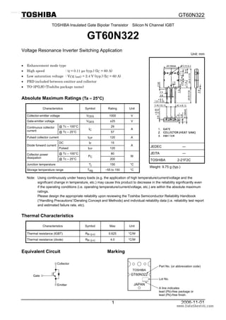
- 1. GT60N322 2006-11-011 TOSHIBA Insulated Gate Bipolar Transistor Silicon N Channel IGBT GT60N322 Voltage Resonance Inverter Switching Application • Enhancement mode type • High speed : tf = 0.11 μs (typ.) (IC = 60 A) • Low saturation voltage : VCE (sat) = 2.4 V (typ.) (IC = 60 A) • FRD included between emitter and collector • TO-3P(LH) (Toshiba package name) Absolute Maximum Ratings (Ta = 25°C) Characteristics Symbol Rating Unit Collector-emitter voltage VCES 1000 V Gate-emitter voltage VGES ±25 V @ Tc = 100°C 29Continuous collector current @ Tc = 25°C IC 57 A Pulsed collector current ICP 120 A DC IF 15 Diode forward current Pulsed IFP 120 A @ Tc = 100°C 80Collector power dissipation @ Tc = 25°C PC 200 W Junction temperature Tj 150 °C Storage temperature range Tstg −55 to 150 °C Note: Using continuously under heavy loads (e.g. the application of high temperature/current/voltage and the significant change in temperature, etc.) may cause this product to decrease in the reliability significantly even if the operating conditions (i.e. operating temperature/current/voltage, etc.) are within the absolute maximum ratings. Please design the appropriate reliability upon reviewing the Toshiba Semiconductor Reliability Handbook (“Handling Precautions”/Derating Concept and Methods) and individual reliability data (i.e. reliability test report and estimated failure rate, etc). Thermal Characteristics Characteristics Symbol Max Unit Thermal resistance (IGBT) Rth (j-c) 0.625 °C/W Thermal resistance (diode) Rth (j-c) 4.0 °C/W Equivalent Circuit Marking Unit: mm JEDEC ― JEITA ― TOSHIBA 2-21F2C Weight: 9.75 g (typ.) Gate Emitter Collector GT60N322 TOSHIBA JAPAN Lot No. A line indicates lead (Pb)-free package or lead (Pb)-free finish. Part No. (or abbreviation code) www.DataSheet4U.com
- 2. GT60N322 2006-11-012 Electrical Characteristics (Ta = 25°C) Characteristics Symbol Test Condition Min Typ. Max Unit Gate leakage current IGES VGE = ±25 V, VCE = 0 ― ― ±500 nA Collector cut-off current ICES VCE = 1000 V, VGE = 0 ― ― 0.1 mA Gate-emitter cut-off voltage VGE (OFF) IC = 60 mA, VCE = 5 V 4.0 ― 7.0 V Collector-emitter saturation voltage VCE (sat) IC = 60 A, VGE = 15 V ― 2.4 2.9 V Input capacitance Cies VCE = 10 V, VGE = 0, f = 1 MHz ― 4200 ― pF Rise time tr ― 0.33 ― Turn-on time ton ― 0.45 ― Fall time tf ― 0.11 0.22 Switching time Turn-off time toff Resistive Load VCC = 600 V, IC = 60 A VGG = ±15 V, RG = 51 Ω (Note 1) ― 0.41 ― μs Diode forward voltage VF IF = 15 A, VGE = 0 ― 1.2 1.9 V Reverse recovery time trr IF = 60 A, di/dt = −20 A/μs ― 0.75 1.7 µs Note 1: Switching time measurement circuit and input/output waveforms 10% 90% VGE VCE IC td (off) toff tr ton 0 0 tf 10%10% 90%90% RG VCC RL 0 www.DataSheet4U.com
- 3. GT60N322 2006-11-013 Collector-emittersaturationvoltage VCE(sat)(V) CollectorcurrentIC(A) Collector-emitter voltage VCE (V) IC – VCE CollectorcurrentIC(A) Collector-emitter voltage VCE (V) IC – VCE CollectorcurrentIC(A) Collector-emitter voltage VCE (V) IC – VCE CollectorcurrentIC(A) Gate-emitter voltage VGE (V) IC – VGE Case temperature Tc (°C) VCE (sat) – Tc 120 0 0 20 40 60 80 100 1 2 3 4 5 6 VGE = 6 V 7 8 20 10 15 Common emitter Tc = -40°C 120 0 0 20 40 60 80 100 1 2 3 4 5 6 VGE = 6 V 7 8 20 10 15 Common emitter Tc = 25°C 120 0 20 40 60 80 100 0 2 4 6 8 10 Tc = 125 °C 4025 Common emitter VCE = 5V 4 0 1 2 3 −60 −20 20 60 100 140 IC = 80 A 10 30 60 Common emitter VGE = 15 V 0 20 40 60 80 100 0 1 2 3 4 5 6 VGE = 6 V 7 8 20 10 15 Common emitter Tc = 125°C 120 www.DataSheet4U.com
- 4. GT60N322 2006-11-014 CollectorcurrentIC(A) Gate-emittervoltageVGE(V) Gate charge QG (nC) VCE, VGE – QG Collector-emittervoltageVCE(V) Gate resistance RG (Ω) Switching Time – RG Switchingtime(µs) Collector current IC (A) Switching Time – IC Switchingtime(µs)CapacitanceC(pF) Collector-emitter voltage VCE (V) C – VCE Collector- emitter voltage VCE (V) Safe Operating Area Collector-emitter voltage VCE (V) Reverse Bias SOA CollectorcurrentIC(A) 30000 10 100 1000 5000 0 10 100 1000 10000 Cres30 50 300 500 3000 10000 Coes Cies Common emitter VGE = 0 f = 1 MHz Tc = 25°C 0.01 1 10 100 1000 0.1 1 5 3 0.03 0.05 0.3 0.5 toff ton tr tf Common emitter VCC = 600 V IC = 60 A VGG = ±15 V Tc = 25°C 70 0.01 1 20 50 0.1 1 10 3 0.03 0.05 0.3 0.5 toff ton tr tf 10 30 40 60 5 Common emitter VCC = 600 V RG = 51 Ω VGG = ±15 V Tc = 25°C 1 1 10 3000 10 100 1000 300 3 5 30 50 IC max (pulsed)* IC max (continuous) 100 1000 500 3 30 300 10 ms * DC operation 1 ms* 100 µs* 10 µs* * Single non-repetitive pulse Tc = 25°C Curves must be derated linearly with increase in temperature. 1 1 10 3000 10 100 1000 300 3 5 30 50 100 1000 500 3 30 300 Tj <= 125°C VGG = 20 V RG = 10 Ω 100 200 0 50 100 150 0 60 120 180 240 VCE = 150 V 50 0 5 10 20 Common emitter RL = 2.5 Ω Tc = 25°C 15 www.DataSheet4U.com
- 5. GT60N322 2006-11-015 1.0 0.0 0.2 0.4 0.6 0.8 Common collector IF = 60 A Tc = 25°C 0 40 80 120 160 200 trr 0 10 20 30 40 50 lrr 1.0 0.0 0.2 0.4 0.6 0.8 Common Collector di/dt = −20 A/µs Tc = 25°C 0 20 40 60 80 trr lrr 5 6 7 8 9 10 Tc = 25°C 10−2 10−5 10−1 10 0 10−4 10−2 10−1 10 0 10 1 10 2 10−3 101 Diode stage IGBT stage Common emitter VGE = 15 V 60 0 25 10 20 30 40 50 50 75 100 125 150 Reverserecoverytimetrr(µs) ForwardcurrentIF(A) TransientthermalimpedanceRth(t) (°C/W) Pulse width tw (s) Rth (t) – tw Case temperature Tc (°C) IC max – Tc MaximumDCcollectorcurrentICmax(A) Forward voltage VF (V) IF – VF PeakreverserecoverycurrentIrr(A) Forward current IF (A) trr, lrr – IF PeakreverserecoverycurrentIrr(A) di/dt (A/µs) trr, lrr – di/dt Reverserecoverytimetrr(µs) 100 0 20 40 60 80 0.0 0.5 1.0 1.5 2.0 2.5 Tc = 125 °C −40 25 Common collector www.DataSheet4U.com
- 6. GT60N322 2006-11-016 RESTRICTIONS ON PRODUCT USE 20070701-EN • The information contained herein is subject to change without notice. • TOSHIBA is continually working to improve the quality and reliability of its products. Nevertheless, semiconductor devices in general can malfunction or fail due to their inherent electrical sensitivity and vulnerability to physical stress. It is the responsibility of the buyer, when utilizing TOSHIBA products, to comply with the standards of safety in making a safe design for the entire system, and to avoid situations in which a malfunction or failure of such TOSHIBA products could cause loss of human life, bodily injury or damage to property. In developing your designs, please ensure that TOSHIBA products are used within specified operating ranges as set forth in the most recent TOSHIBA products specifications. Also, please keep in mind the precautions and conditions set forth in the “Handling Guide for Semiconductor Devices,” or “TOSHIBA Semiconductor Reliability Handbook” etc. • The TOSHIBA products listed in this document are intended for usage in general electronics applications (computer, personal equipment, office equipment, measuring equipment, industrial robotics, domestic appliances, etc.).These TOSHIBA products are neither intended nor warranted for usage in equipment that requires extraordinarily high quality and/or reliability or a malfunction or failure of which may cause loss of human life or bodily injury (“Unintended Usage”). Unintended Usage include atomic energy control instruments, airplane or spaceship instruments, transportation instruments, traffic signal instruments, combustion control instruments, medical instruments, all types of safety devices, etc.. Unintended Usage of TOSHIBA products listed in his document shall be made at the customer’s own risk. • The products described in this document shall not be used or embedded to any downstream products of which manufacture, use and/or sale are prohibited under any applicable laws and regulations. • The information contained herein is presented only as a guide for the applications of our products. No responsibility is assumed by TOSHIBA for any infringements of patents or other rights of the third parties which may result from its use. No license is granted by implication or otherwise under any patents or other rights of TOSHIBA or the third parties. • Please contact your sales representative for product-by-product details in this document regarding RoHS compatibility. Please use these products in this document in compliance with all applicable laws and regulations that regulate the inclusion or use of controlled substances. Toshiba assumes no liability for damage or losses occurring as a result of noncompliance with applicable laws and regulations. www.DataSheet4U.com