1. M-Power 2A Series of Multi-chip Power Devices 81
Takayuki Shimatoh
Noriho Terasawa
Hiroyuki Ota
M-Power 2A Series of Multi-chip
Power Devices
1. Introduction
Fuji Electric has developed highly efficient and
low-noise proprietary multi-oscillated current resonant
circuits for use in switching power supplies. As a cus-
tom device for this circuit, Fuji Electric has commer-
cialized the “M-Power 2”, housed in a small package
(SIP23) containing a control IC and two power MOS
FETs (metal oxide semiconductor field effect transis-
tors), and this device has been well received for use in
power supplies for flat panel televisions. As a result of
the trend toward increasingly larger sizes of flat panel
televisions in recent years, large capacity power sup-
plies (having an output power of approximately 400 W)
are being required. To support even larger capac-
ity power supplies, Fuji Electric has developed the M-
Power 2A series of devices provided with power MOS
FETs having a lower ON-resistance, and featuring im-
proved control IC functionality.
This paper introduces the M-Power 2 series and
the M-Power 2A series of multi-chip power devices, and
the operating principles of the multi-oscillated current
resonant power supply, to which these devices are ap-
plied.
2. Operating Principles of the Multi-oscillated
Current Resonant Converter
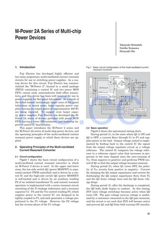
2.1 Circuit configuration
Figure 1 shows the basic circuit configuration of a
multi-oscillated current resonant converter in which
an M-Power 2 device is used. In the upper and lower
arms, the low-side switch Q1 (power MOSFET) is sepa-
rately-excited (PWM controlled) and is driven by a con-
trol IC and the high-side switch Q2 (power MOSFET)
is self-excited and is driven by an auxiliary winding
P2 of an isolated transformer Tr, and current resonant
operation is implemented with a series resonant circuit
consisting of the Tr leakage inductance and a resonant
capacitor Cr. P2 and the Vcc control winding P3, which
supplies power to the control IC, are designed to be
tightly coupled to P1, and each generates a voltage pro-
portional to the P1 voltage. However, the P2 voltage
has the reverse phase of the P1 voltage.
2.2 Basic operation
Figure 2 shows the operational timing chart.
During period (1), in the state where Q1 is ON and
Q2 is OFF, a current flows through Cr to P1 and sup-
plies power to the load. Output voltage control is imple-
mented by feeding back to the control IC the signal
from the output voltage regulator circuit as a voltage
reference. The control IC compares the voltage refer-
ence to a reference signal value that increases in pro-
portion to the time elapsed since the zero-crossing of
VP1 (from negative to positive) and performs PWM con-
trol of Q1 so that the output voltage becomes constant.
During period (2), when Q1 turns OFF, the polar-
ity of VP1 inverts from positive to negative. Current
for charging the Q1 output capacitance and current for
discharging the Q2 output capacitance flows from Tr,
and the Q1 drain voltage rises and the Q2 drain volt-
age drops.
During period (3), after the discharge is completed,
the Q2 body diode begins to conduct. At this timing,
ZVS (zero voltage switching) becomes active when Q2
turns ON. The gate voltage turn-on voltage is moder-
ated by a resistance connected to the Q2 gate terminal,
and the circuit is set such that ZVS will become active
and prevent Q1 and Q2 from both turning ON simulta-
Fig.1 Basic circuit configuration of the multi-oscillated current
resonant converter
+
M-Power 2
PWM control
Self-oscillator
Tr
Cr
R2
P2
P1
S2
S1
D2
D1
R1
Q2
Q1
Output voltage
regulator circuit
Normal/ standby signal
Control IC
+
+
P3
IQ2
ID2
IQ1
ID1
VQ2
VG2
VQ1
VP1 VO
VG1
Ed
RectifierorPFC
IIIC.CC
2. Vol. 53 No. 3 FUJI ELECTRIC REVIEW82
neously and a short-circuit current from flowing. Also,
with Q2 in an ON state, a current, inverted from that
of period (1), flows to P1 and supplies power to the
load.
Operation during period (4) is the same as during
period (2). Afterwards, the operation returns to period
(1), and when discharging is completed, the Q1 body
diode begins to conduct. At this timing, ZVS becomes
active when Q1 turns ON. After the timing of the
negative to positive zero-crossing of VP1 is indirectly
detected by the P3 voltage, and after the time Td, dead
time for prevention of an arm short, has elapsed, Q1 is
turned ON.
2.3 Features
The converter has the following features.
(1) High efficiency
(2) Low noise
(3) No arm-short by lower frequency side operation
(the resonant breakaway phenomenon)
(4) High efficiency during light load operation
Features (1) and (2) above provide the same benefit
as the conventional current resonant circuit frequency
control method. However, features (3) and (4) are diffi-
cult to achieve with the frequency control method, and
a significant advantage of the present method is the
ability to provide these countermeasures and improve-
ments easily.
3. Overview of the M-Power 2A Series
Figure 3 shows the appearance of the M-Power 2
and M-Power 2A series devices. These devices use the
same package construction. The M-Power 2A series
features improved control IC functionality, and its pin
layout differs from that of the M-Power 2 series.
3.1 Structure
Internally, the M-Power 2A has an all-silicon
multi-chip configuration, and the M-Power 2A houses
a control IC and two power MOSFETs (Q1 and Q2) in
a SIP package having a height of 10 mm and width of
30 mm, which is suitable for application to low-profile
power supplies.
3.2 Control IC functions
The control IC, which was developed specially for
multi-oscillated control, has some general functions.
One is a computation function to control the PWM
(pulse width modulation) operation of the Q1 accord-
ing to the indicated value for the secondary side output
voltage. The other is a protection function by latched
shutdown against the overcurrent, load short-circuit,
overheat, overvoltage and undervoltage lockout. Also,
the latched shutdown function of the overcurrent pro-
tection and the overheat protection is provided with a
timer setting.
3.3 Power MOSFET
The power MOSFET used is a SuperFAP-G series
power MOSFET having the characteristics of low-re-
sistance and high switching speed, and aims to reduce
loss.
4. Improvements to the M-Power 2A and Differ-
ences from the M-Power 2 Series
The improvements to the M-Power 2A and differ-
ences from the M-Power 2 series are as listed below.
4.1 Structural improvements
Compared to the lead frame structure of the M-
Power 2, the M-Power 2A has a larger mounting area
for the power MOSFETs (Q1 and Q2), and enables
the mounting of power MOSFETs having lower ON-
Fig.3 Appearance of M-Power 2 and M-Power 2A series de-
vices
M-Power 2 series
M-Power 2A series
Fig.2 Operational timing chart
Voltage refer-
ence value,
Reference
signal value
Gate
threshold
voltage
0
0
0
0
0
0
0
VG1
Voltage reference value
Reference signal value
(1) (3)
(2) (4)
VP2
Dead time for prevention of arm short Td
VG2
VQ2 VQ1
VP3
VP1
ID1 ID2
IQ1 IQ2
VP2 , VG2
VQ1 , VQ2
VP1 , VP3
IQ1 , IQ2
ID1 , ID2
3. M-Power 2A Series of Multi-chip Power Devices 83
Table 1 Functional comparison of M-Power 2 and M-Power
2A
Item M-Power2
Input power
at standby
(when Po = 0 W)
M-Power2A
0.6 W
(burst operation)
0.41 W
(burst operation)
Switching
restart timing
Minimum of
CB oscillation
FB voltage
reaches VthFB
Dead time for
prevention of
arm short
Fixed Adjustable
Circuit to prevent
audible noise at
light load
External circuit Built-in
Overvoltage
protection (OV)
1 shot latch
Timer latch
at 270 μs
Overcurrent
protection (OC)
Plus detection
(+900 mV)
Minus detection
(-171 mV)
Short circuit
protection (SC)
Plus detection
(+1,500 mV)
1 shot latch
No function
Timer latch at 100 ms Timer latch at 36 ms
Built-in
standby mode
External
standby circuit
resistance (in order to ensure sufficient current capac-
ity, the provision of two main current terminals). As a
result, the MP2A5038 (500 V/0.38 Ω) is well suited for
application to output switching power supplies of ap-
proximately 400 W.
4.2 Control IC function and performance improvements
Table 1 compares the functions of the M-Power 2
and the M-Power 2A.
(1) Improved output voltage dropout characteristics
at sudden change in load
In the case of unloaded burst operation as shown in
Fig. 4 for a power supply equipped with an M-Power 2
device, if the load is suddenly changed to a near maxi-
mum loaded condition, a phenomenon occurs in which
the output voltage drops significantly. The voltage
drop occurs because after a sudden load change (from
no load to maximum load) during burst operation, even
if the output voltage reference value, COMP voltage
(FB (feedback) voltage in the case of the M-Power 2A),
rises, switching does not restart unless the CB (burst
operation frequency) oscillation reaches its lower limit.
Thus the M-Power 2A has been devised such that
switching restarts soon after the point in time when
the FB voltage rises, and therefore there is almost no
drop in output voltage, and a dramatic improvement is
realized.
(2) Surge voltage prevention of the overvoltage pro-
tection
The M-Power 2’s overvoltage protection operates to
instantaneously implement a latched shutdown when
an excessive voltage (overvoltage) is input. However,
it is desired that latched shutdown does not occur
for an overvoltage pulse having an extremely narrow
width, such as a lightening surge. Therefore, with the
M-Power 2A, the overvoltage protection function is pro-
vided with a 270 µs timer, and does not react to narrow
width overvoltage pulses.
(3) Less resistive loss for overcurrent protection detec-
tion
With the M-Power 2 series, overcurrent protection
circuit has an operating voltage of 900 mV, the current
detection resistance loss increases as the power supply
output power increases, and increasing the size of the
detection resistor results in greater heat generation.
On the other hand, the M-Power 2A has a lower operat-
ing voltage of 171 mV, and achieves reduced detection
resistance loss. The following improvements have been
made in the M-Power 2A.
(a) The current detection method has been
changed from plus to minus, and the influence
of the power MOSFET’s drive current has been
eliminated.
(b) The current detection terminal is separated
from the power MOSFET’s source terminal,
and an externally attached filter can be de-
signed freely in accordance with the power sup-
ply specifications.
(c) Two GND terminals (PGND and SGND) are
provided, the influence of noise on the control
IC lessened, and the pattern layout has been
made easier to design.
(4) Built-in compensation circuit for light load burst
Fig.4 Schematic drawing of operation at sudden load change
M-Power 2
M-Power 2
M-Power 2A
Delay time
COMP (M-Power 2)
FB (M-Power 2A)
CB (M-Power 2)
IO (load current)
VO (output voltage)
(M-Power 2A)
VDS (Q1)
(M-Power 2)
VDS (Q1)
Vcomp
VthFB
M-Power 2A
4. Vol. 53 No. 3 FUJI ELECTRIC REVIEW84
operation
With the M-Power 2, the operation is burst dur-
ing a light load, and in cases where an audible burst
operation sound from Tr creates a problem, it is recom-
mended that a circuit be attached externally to provide
a solution. On the other hand, with the M-Power 2A,
a compensation circuit for burst operation is built-in,
thereby enabling a reduction in the number of exter-
nally attached components.
(5) Reduced power consumption of control IC
The M-Power 2 has a built-in standby function, but
the M-Power 2A eliminates this function in order to
reduce the consumption of electrical power by the con-
trol IC. However, in the case where a standby function
is required in one converter, a standby function circuit
can be attached externally. (See Fig. 5.)
5. Conclusion
This paper has introduced the newly developed M-
Power 2A series of products that feature an improved
control IC for power supplies in flat panel televisions
and the like (Table 2). Accordingly, the M-Power 2A
series of devices are well suited for application to large
capacity power supplies for use in large screen flat
panel televisions and the like. In the future, Fuji Elec-
tric plans to expand the product lineup to support vari-
ous other requests. Fuji Electric also intends to strive
to develop power supply systems and to commercialize
custom power devices in order to support requests for
even more sophisticated power supplies.
Table 2 Fuji Electric’s M-Power 2A series product lineup
MOSFET
(Q1, Q2)Model name Package
Control IC
500 V 16.5 V SIP23
125 to
150°C
VDS RDS (ON) VCC (ON) Tj (OFF)
MP2A5038 0.38 Ω
MP2A5050 0.50 Ω
MP2A5060 0.60 Ω
MP2A5077 0.77 Ω
MP2A5100 1.0 Ω
MP2A5135 1.35 Ω
Fig.5 External standby circuit
+
External
standby
circuit
PC2 PC1
PC1
VCC
FB
Q2
Q1
Control
IC
Regulator
VW
VREF
CON
IS
S
D2
G2
GND
+
+
D1
M-Power 2A
+