Maximizing Efficiency in Low-Profile Power Supplies
1. Maximizing efficiency in a low-profile form factor is a non-trivial chal-
lenge for even the most experienced power supply designers. Some
examples of systems requiring low-profile power supply designs
include: flat panel displays, rack mounted computer equipment and
telecom and aerospace chassis-mounted assemblies. Equipment in
this class can require several hundred watts of power delivered to the
load at any given time. For example, a typical 12V, 300W power sup-
ply used in a 1U rack mounted application has a maximum height
restriction of 1.75 inches (44.45 mm) and would include forced air
cooling available from 1 or more fans. But for systems with height
restrictions less than 1U, forced air cooling may not be possible,
which means the heat dissipated must be managed using costly, low-
profile heat sinks with large surface area. Therefore, designing for the
highest efficiency is critical because it has a direct impact on reduc-
ing the size and cost of the heat sinks and increasing the overall reli-
ability of the design.
In most cases, AC-DC power supplies operating at these power lev-
els will require some type of active power factor correction (PFC).
The necessity for PFC can be driven by one or more criteria includ-
ing: power level, end application, equipment class and geographical
location and is usually guided by specifications such as EN6100-3-2
or IEEE 519. For an AC-DC power supply, a non-isolated, off-line,
boost pre-regulator is normally used as the PFCstage where its DC
output voltage is seen as the input to a downstream, isolated DC-DC
converter. Since two converters appear in series with each other, the
overall system efficiency, çSYS, is defined by the product of the indi-
vidual converter efficiencies.
(1)
From equation (1) it is apparent that careful consideration must be
given toward choosing the best power topologies
and control techniques for both converter stages. One system solu-
tion that has many interesting high efficiency characteristics is the
combination of an interleaved dual boundary conduction mode (BCM)
PFC followed by an asymmetrical half-bridge (AHB), isolated DC-DC
converter using a current doubler rectifier secondary with self-driven
synchronous rectifiers (SR).
For PFC converters in the 300W-1kW range, interleaved boundary
conduction mode (BCM) PFC should be considered due its higher
efficiency compared to continuous conduction mode (CCM) PFC con-
trol at similar power levels. Interleaved BCM PFC is based upon a
variable frequency control algorithm where two PFC boost power
stages, are synchronized 180 degrees out of phase with respect to
each other. The high peak currents normally seen by the EMI filter
and PFC output capacitor are thereby reduced due to the effective
inductor ripple current cancellation. The output PFC bulk capacitor
benefits from ripple current cancellation because the AC RMS current
flowing through the equivalent series resistance (ESR) is reduced.
Further efficiency benefits are realized since the boost MOSFETs
turn off under AC line-dependant zero voltage switching (ZVS) and
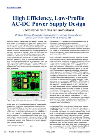
turn on under zero current switching (ZCS). For a 350W interleaved
BCM PFC design, MOSFET heat sinks can be eliminated as can be
seen in Figure 1. Conversely, the boost MOSFET used in a CCM
PFC design is subjected to frequency dependant switching losses
that are proportional to input current and line voltage. By switching
the interleaved BCM boost diodes off at zero current, there are no
reverse recovery losses. Eliminating reverse recovery losses allows
the use of less expensive, fast recovery rectifier diodes and can
remove the need for heat sinking in some cases. For a CCM PFC
design, reverse recovery losses are unavoidable and often dealt with
by applying an RC snubber across the diode, which will lower effi-
ciency or specifying higher performance, silicon carbide diodes,
which have higher associated costs.
For the isolated DC-DC converter design, the half-bridge is a good
topology choice since there are two complementary driven, primary
side MOSFETs and the maximum drain-to-source voltage is limited to
the applied DC input voltage. Two variations of the half-bridge, known
as the LLC and asymmetrical half-bridge (AHB), are widely used part-
ly due to the availability of power management control IC’s uniquely
dedicated to these topologies. The LLC takes advantage of the para-
sitic elements associated with the power stage design to achieve ZVS
using a variable frequency control technique. However, because the
regulated DC output only uses capacitive filtering, this topology is
best suited for lower output ripple, higher output voltage applications.
As a general guideline for off-line, DC-DC applications the LLC tends
to be favored when the output voltage is greater than 12VDC.
ߟௌௌ ൌ ߟி ൈ ߟି
P O W E R S U P P LY
52 Bodo´s Power Systems® May 2010 www.bodospower.com
High Efficiency, Low-Profile
AC-DC Power Supply Design
There may be more than one ideal solution
By Steve Mappus, Principal Systems Engineer, Fairchild Semiconductor,
Power Conversion America, PCIA, Bedford, NH
Figure 1: 12V, 300W, Low-Profile, Universal AC-DC Power Supply
2. The AHB is an efficient choice for a 300W, 12V DC-DC converter. A
fixed frequency control method is used, where the primary current
naturally lags the transformer primary voltage, providing the neces-
sary condition for ZVS of both primary MOSFETs. Similar to the LLC,
the ability to achieve ZVS with the AHB relies upon a thorough
understanding of circuit parasitic elements such as transformer leak-
age inductance, winding capacitance and junction capacitance of dis-
crete power devices. Compared to the variable frequency control
method used for LLC control, fixed frequency operation greatly sim-
plifies the task of secondary side, self-driven SR. The self-driven, SR
gate drive voltages are easily be derived from the transformer sec-
ondary. Adding a low-side MOSFET driver, such as the Dual 4A,
FAN3224 shown in Figure 2, provides accurate level shifting and high
peak drive current through the MOSFSTs Miller plateau region to
assure fast, efficient SR switching transitions.
The current doubler rectifier can be applied to any double-ended
power topology and for high DC current applications, it has several
noteworthy attributes. First, the secondary consists of a single wind-
ing, simplifying the transformer structure. Second, since the required
output inductance is divided between two inductors, the power dissi-
pated due to the high current flowing in the secondary is distributed
more efficiently. Third, the individual inductor ripple currents cancel
each other as a function of duty cycle (D). The cancelled sum of the
two inductor currents has an apparent frequency equal to twice the
switching frequency allowing higher frequency; lower peak current
flowing into the output capacitor. And finally, in a symmetrical convert-
er (push-pull, half-bridge, full-bridge), each current doubler inductor
would carry half the output current but for the AHB this is not exactly
the case.
If unaccounted for, the asymmetrical voltage applied to the secondary
side rectifiers can be one of the AHB drawbacks. When the AHB is
operated near its limit of D=0.5, the applied SR voltages are nearly
matched. However, it is more reasonable that the transformer turns
ratio be designed such that D is within the practical range of
0.25<D<0.35 during nominal operation. When D is within this range,
the voltage stress between Q1 and Q2 and the applied voltage
across L1 and L2 become imbalanced, resulting in an uneven current
distribution between L1 and L2. Similarly, the voltage ratings for each
SR MOSFET must also be considered. For this reason, it may be
acceptable to use inductors L1 and L2 that are not equal in value and
SR MOSFETs that have different voltage ratings. The transformer
turns ratio can also be wound asymmetrically but these techniques
require a detailed understanding of the circuit behavior under all
operating conditions.
To demonstrate the feasibly of the recommended solution, the speci-
fications shown in Table 1 were met using an interleaved dual BCM
PFC boost, pre-regulator followed by an asymmetrical half-bridge,
DC-DC converter with self-driven SR, as pictured in Figure 1.
The specifications shown in Table 1 are a simplified summary of the
full design requirements. The primary design goals are to:
• Maximize efficiency over the widest range possible
• Achieve lowest possible design profile
• Minimize size and use of heat sinks
Maximizing efficiency over the widest possible load range requires
careful consideration when choosing materials and components for
each power stage, particularly in the area of magnetics design.
Because the frequency for the interleaved BCM PFC can reach sev-
eral hundred kHz, and vary by as much as 10:1, the boost inductors
need to be custom designed. Using a properly rated, equivalent
gauge litz wire gives best results for minimizing AC losses that can
dominate copper loss in a BCM PFC boost inductor. A gapped ferrite
material suitable for high frequency operation should be used and for
this example, N87 material from EPCOS was chosen on a low-profile
P O W E R S U P P LY
Figure 2. FAN3224, Self-Drive SR with Current Doubler Rectifier
Table 1: Low-Profile, AC-DC Power Supply Design Specifications
%227+
ZZZWUDQVLFFRP
%
%LSRODU 6LOLFRQ DUELGH WUDQVLVWRUV
)RU KLJK HI¿FLHQF DQG KLJK WHPSHUDWXUH
9 $ DQG $ DW Û RSHUDWLRQ
3. EFD30 ferrite core set. Measured efficiency results for the PFC are
shown in Figure 3.
One solution for a 300W, low-profile, AHB transformer requires two
horizontal core structures, where the primary windings are connected
in series and the secondary windings connected in parallel. The use
of two transformers is necessary because the cross sectional area,
Ae, of each core is nearly half of the 150mm2 required to avoid satu-
ration. Finding a single, conventional core shape with a 150mm2
cross section would not be possible in a less than 20mm low-profile
component. Similar to the BCM PFC inductor design, litz wire and a
high frequency ferrite core material are used to maintain high efficien-
cy. A final important design step is controlling the amount of allowable
leakage inductance in the AHB transformer. Some value of leakage
inductance is required for ZVS and adjusting the timing delay for the
self-driven SR. For this design the effective leakage due to both
transformers was optimized to 7μH or 1.5% of the total effective mag-
netizing inductance. Measured efficiency results for the 300W AHB
DC-DC converter are shown in Figure 4.
Full load efficiency is dominated by conduction losses through the
converters power stage so there is little a controller can do to help
under these conditions. However, there are several controller tech-
nologies that should be considered for maintaining higher light load
efficiency. The FAN9612, an interleaved dual BCM PFC controller,
limits frequency-dependent Coss MOSFET switching losses at light
load and near the zero crossing of the AC input voltage by utilizing
an internal fixed maximum frequency clamp. During the portion of the
AC line voltage for VINVOUT/2, Coss capacitive switching losses are
reduced through a valley-switching technique used to sense the opti-
mal MOSFET turn-on time. Conversely, when VINVOUT/2, the PFC
boost MOSFETs always turn-on under ZVS conditions. Light load effi-
ciency improvements are further attained by introducing an automatic
phase management feature that reduces operation from dual channel
to single channel mode. The light load efficiency advantage from
phase management can be seen in Figure 3 for 10%POUT20%,
where the efficiency “curve” appears more flat. Operating in single
channel mode minimizes the impact of switching losses on light load
efficiency. The ability of the interleaved PFC to maintain synchroniza-
tion during phase management is shown in Figure 5. The left-sided
plot was recorded when transitioning from single channel to two
channel operation as the load is increased from zero to 19% (64W).
Similarly the right-sided plot was recorded when transitioning from
dual channel to single channel operation while the load is decreased
from full load to 12% (42W).
The implementation of the AHB isolated DC-DC converter is
achieved using the FSFA2100, AHB controller, which integrates the
pulse width modulation (PWM) control, gate drive functionality and
internal power MOSFETs into a single 9 pin SIP power package. This
advanced level of packaging and integration allows designers to
achieve very high efficiency up to 420W, using fewer external compo-
nents. Combining these three critical functions into a single package
eliminates the task of programming the dead time required for ZVS
and minimizes gate drive parasitic inductance between the internal
driver and MOSFETs. Most of the power dissipated within the SIP
power package is due to the switching internal MOSFETs, so a low
profile extruded heat sink is required, especially for a 300W design
with no available forced air cooling.
The total AC-DC system including, the input EMI filter, bridge rectifier,
interleaved BCM PFC and AHB DC-DC yields a measured overall
efficiency as shown in Figure 6. The design achieves 91% peak effi-
ciency for Vin=120VAC, 92% peak efficiency for Vin=230VAC and
greater than 90% for Vin=120VAC or 230VAC, POUT38% (114W).
Magnetic component design, power semiconductor selection, pcb
layout, choice of heat sinks and controller features all must work per-
fectly together for a successful low-profile AC-DC power supply
design demonstrating high efficiency over a wide load range.
Depending upon system requirements, there may be more than one
ideal solution best suited for a particular application. The design dis-
cussed herein is just one example for achieving high efficiency from
a universal AC input to 12V, 300W design requiring PFC and a low
profile of only 18mm total height.
PCIM Booth 12/601
www.Fairchildsemi.com
54 Bodo´s Power Systems® May 2010 www.bodospower.com
P O W E R S U P P LY
Figure 4: AHB 390V to 12V/25A, DC-DC Measured Efficiency
(100%=300W)
Figure 5: PFC Phase Management (1→2, 19%=64W and 2→1,
12%=42W)
Figure 6: Total Measured System Efficiency (EMI Filter Included)
Figure 3: Interleaved BCM PFC Measured Efficiency (100%=330W)