This document presents a design of a comparator circuit based on an operational transconductance amplifier (OTA) using 22 nm FinFET technology, which enhances performance for high-frequency applications. The comparator exhibits substantial gain (>100 dB), a phase margin of 65°, and a common mode rejection ratio above 70 dB, making it suitable for high sampling rate data converters. The research emphasizes the advantages of FinFETs over traditional MOSFETs in analog and mixed-signal circuit applications.
![International Journal of Electrical and Computer Engineering (IJECE)
Vol. 12, No. 2, April 2022, pp. 2158~2168
ISSN: 2088-8708, DOI: 10.11591/ijece.v12i2.pp2158-2168 2158
Journal homepage: http://ijece.iaescore.com
Operational transconductance amplifier-based comparator for
high frequency applications using 22 nm FinFET technology
Vasudeva Gowdagere1
, Uma Bidikinamane Venkataramanaiah2
1
Department of Electronics and Communication Engineering, RV College of Engineering, Bangalore, India
2
Department of Electronics and Communication Engineering, RV College of Engineering, Visvesvaraya Technological University,
Belgaum, India
Article Info ABSTRACT
Article history:
Received Mar 30, 2021
Revised Dec 3, 2021
Accepted Dec 15, 2021
Fin field-effect transistor (FinFET) based analog circuits are gaining
importance over metal oxide semiconductor field effect transistor (MOSFET)
based circuits with stability and high frequency operations. Comparator that
forms the sub block of most of the analog circuits is designed using
operational transconductance amplifier (OTA). The OTA is designed using
new design procedures and the comparator circuit is designed integrating the
sub circuits with OTA. The building blocks of the comparator design such as
input level shifter, differential pair with cascode stage and class AB amplifier
for output swing are designed and integrated. Folded cascode circuit is used
in the feedback path to maintain the common mode input value to a constant,
so that the differential pair amplifies the differential signal. The gain of the
comparator is achieved to be greater than 100 dB, with phase margin of 65°,
common mode rejection ratio (CMRR) of above 70 dB and output swing from
rail to rail. The circuit provides unity gain bandwidth of 5 GHz and is suitable
for high sampling rate data converter circuits.
Keywords:
Comparator
Fin field-effect transistor
High frequency
Layout design
Operational transconductance
amplifier
Rail-to-rail This is an open access article under the CC BY-SA license.
Corresponding Author:
Vasudeva Gowdagere
Research Scholar, Electronics and Communication Engineering Department, RV College of Engineering
Bangalore-560059, India
Affiliated to Visvesvaraya Technological University, Belagavi, Karnataka, India
e-mail: devan.vasu921@gmail.com
1. INTRODUCTION
Mixed signal circuit design is gaining importance in most of the system on chip (SOC) that is used in
every electronic system operating at few GHz. Operational transconductance amplifier (OTA) is one of the
primary building blocks of analog and mixed signal circuits that is used as sub system in every circuit design.
Design of OTA requires estimating the W/L geometries of transistors to meet performances such as DC gain,
unity-gain bandwidth (UGB), common mode rejection ratio (CMRR), slew rate (SR), input common-mode
voltage (VICM) and power dissipation. Process variation and nonlinear behavior of metal oxide semiconductor
field effect transistor (MOSFETs) have been a challenging task to be addressed by circuit design engineers.
Devices such as multi-gate MOSFET, Fin field-effect transistor (FINFETs), ultra-thin body silicon on insulator
are gaining prominence in replacing MOSFETs for all mixed signal circuit design [1]. FinFET is demonstrated
to be more advantages than MOSFET with additional gate control input, attenuated drain induced barrier
lowering (DIBL), improved sub threshold swing and immunity to short channel effects [2]. FinFET based
analog circuits are designed and demonstrated to be advantageous over MOSFETs [3]. Two stage amplifiers
are designed using FinFET and is observed to be having advantageous over MOSFET based op-amp [4].
FinFET has been recognized as a hopeful device as it enables additional gate length scaling due to its superior
immunity to short channel effect by making the channel controlled by gate from more than one side [5].](https://image.slidesharecdn.com/11125527emr21jul30mark-220628024625-4ed6bfe9/75/Operational-transconductance-amplifier-based-comparator-for-high-frequency-applications-using-22-nm-FinFET-technology-1-2048.jpg)
![Int J Elec & Comp Eng ISSN: 2088-8708
Operational transconductance amplifier-based comparator for high frequency … (Vasudeva Gowdagere)
2159
OTA circuit design using FinFET with 32 nm silicon on insulator (SOI) model is presented in [6]
demonstrating its performance metrics. Sohn et al. [7] have presented general guidelines for design of analog
circuits based on FINFETs. Threshold voltage in FinFET imposes limitations in analog circuit design and to
overcome these bulk driven (BD) floating gate (FG) method is presented by Khateb [8]. In order to reduce
power dissipation and to increase output swing self-biasing technique is used in circuit design [9]. Low power
analog circuits are designed considering DC shifting and BD differential technique with rail-to-rail OTA [10].
FinFET based OTA is designed for low power applications using three stage structure and the design using
32 nm model that is found to operate at maximum frequency of 20 MHz, UGB and gain of 64 dB with a 33°
phase margins [11]. A class AB tunable transconductor featuring low quiescent power consumption and the
circuit features good dynamic performance with low distortion is presented in [12].
A pseudo-differential fully balanced, fully symmetric CMOS OTA architecture with inherent
common mode detection is presented in [13]. An ultra-low power recycling folded cascode OTA which
employs a power reduction technique that substantially reduces the power consumption while satisfying the
gain and bandwidth requirements is presented in [14]. A simple rail-to-rail CMOS Miller OTA topology for
ultra-low-voltage and ultra-low-power applications using DC shifting and BD differential pair configuration is
presented in [15]. The concept of programmable FG-OTAs as well as building second order sections using
these amplifiers is discussed in [16]. By combining the techniques pseudo differential pair and the bulk driven
MOS transistors the OTA proposed for ultra-low voltage operation is presented in [17].
A new architecture for improvement of slew rate for an input signal with a rise time an OTA in FinFET
technology is presented in [18]. One of the most commonly used low voltage output buffers was proposed by
Monticelli [19]. A simple single stage OTA which is also known as five transistor OTA is presented in [20].
OTA based circuits are gaining importance in analog circuit applications such as filters, converters, and
oscillators. The use of FinFET based OTA exhibits better performance in comparison to conventional CMOS
based OTA is discussed in [21]. In this paper, comparator circuit which forms the sub system in every data
converter circuit is designed using OTA from basic principles and is evaluated for its performances to operate
at high frequencies. Section 2 discusses FinFETs and its fundamentals detailing device parameters and small
signal model. Section 3 discusses OTA concepts, internal structure, design specifications and design of OTA.
Section 4 discusses comparator design based on OTA. Section 5 discusses modeling of OTA and comparator.
Results and discussion are presented in section 6 and conclusion is presented in section 7.
2. FinFET
Double gate FinFET device shown in Figure 1(a) and its characteristics demonstrating the increased
current flow in the channel by controlling with two gate voltage is presented in [22]. Small signal model for
the DG FET is presented in Figure 1(b). Cgd, Cgs and Cds are the parasitics in FinFET that limits the device
operation at high frequencies and Rgd, Rgs, Rds and Rsub limits the device for low power operations.
Predictive technology model (PTM) parameters for FinFET presented in Table 1 and the
corresponding model files are considered for design of OTA and OTA based comparator. Considering
structural and electrical parameters of FinFET device modeling is carried out for analysis of input and output
characteristics. The theoretical and practical mismatches are identified based on simulation results and the
appropriate geometry settings for FinFET is identified for maximum frequency of operation and low power
dissipation.
(a) (b)
Figure 1. FinFET, (a) FinFET device-structure of DGFET [22] and (b) small signal model [22]](https://image.slidesharecdn.com/11125527emr21jul30mark-220628024625-4ed6bfe9/75/Operational-transconductance-amplifier-based-comparator-for-high-frequency-applications-using-22-nm-FinFET-technology-2-2048.jpg)
![ ISSN: 2088-8708
Int J Elec & Comp Eng, Vol. 12, No. 2, April 2022: 2158-2168
2160
Table 1. FinFET device parameters
Parameter Value
Channel length 22 nm
Oxide thickness 1 2.5 nm
Oxide thickness 2 2.5 nm
Gate length 22 nm
Source/drain extension length 50 nm
Gate to source/drain overlap 2 nm
Work function 4.6 eV
Source/Drain doping 1 1019
cm–3
Dielectric constant of channel 11.7
Dielectric constant of insulator 3.9
Band gap 1.12 eV
Affinity of channel material 4.05 eV
Mobility of electrons 1400 cm2
/Vs
Saturation velocity 1.07e + 07 cm/s
3. OTA DESIGN
The primary building blocks of OTA are presented in Figure 2. The input stage performs level shifting,
second stage is the folded cascode stage with feedback and the last stage is the output stage. OTA connected
in the unity gain configuration the operating signal swing is limited by the common-mode range of the input
stage and the allowable output signal range. To allow maximum signal amplitudes, the rail-to-rail voltage
ranges should extend from the positive supply to the negative supply levels. A simple class-AB amplifier is
used as the output stage to an amplifier, allowing rail-to-rail output signal swing [23]. The simple OTA circuit
is presented in Figure 3 that is realized using eleven transistors. The transistors F1 and F2 are the differential
pair and forms the transconductance cell that converts the input voltage V+in and V–in (differential input
voltages) to current. The differential current output (Iout) of the differential pair is converted to single ended
current at the output by using the current mirrors F3 to F8, F10 and F11. F9 transistor is used to bias the
differential pair and is used as current sink circuit. The cut-off frequency of the OTA is decided by setting the
appropriate bias current and the load capacitance of the OTA. The transconductance gain gm of the OTA is
controlled by setting the current that enters the transistor F9 and the gate voltage Vb is appropriately set. Design
of OTA is primarily identifying the transistor geometries such that the simulation results are matching the hand
calculations. A systematic procedure for the design of a single stage OTA using gm/ID methodology is
discussed in [24]. Design methodology based on gm/ID method is the most popular approach that identifies
the transistor geometries based on data sheets and simulation results. In this method of design of OTA circuits
based on datasheet several design variables that were required for the design were assumed without clear rules.
The design specifications meeting input range, common mode rejection and noise parameters were not
considered in this approach. Even the channel length variations with regard to gm/ID were not considered in
the design process. Considering the limitations of designing OTA circuit, a detailed approach that is based on
gm/ID method is presented in this work with necessary modifications for design of simple OTA. The design
approach presented in this work considers both design and optimization procedures considering small signal
model of FinFET and device parameters. Table 2 presents the specifications considered for OTA design.
The maximum current that is available at the OTA bias is considered as 20 μA and the gain bandwidth
product (GBW) is assumed to be approximately equal to closed loop bandwidth (BMCL) and the buffer input
range is considered as common mode input range. Design of OTA is considered using step by step procedure.
In step 1 the input pair is designed considering the input range assumed to be close to the ground rail between
0.15 to 1.05 V. With (1) the transconductance of the differential pair is determined [25]. The internal parasitics
are considered for accurate calculation of gm.
𝐺𝐵𝑊 =
g𝑚1,2
2𝜋𝐶𝐿
(1)
Substituting GBW and CL in (1) gm is approximated to 160 µS. Considering the OTA bias current of
20 μA which is split as the current flows through F1 and F2 is considered as 16 S/A(gm/ID1,2). The DC gain
of the OTA considering differential signaling is given by (2),
𝐴𝑣𝑑𝑐 =
g𝑚1,2
(g𝑑𝑠2+g𝑑𝑠4)
(2)
Considering gm/ID1,2 and the Avdc parameter (open loop DC gain is 32 dB) the requirements for maintaining
output conductance is given as in (3).](https://image.slidesharecdn.com/11125527emr21jul30mark-220628024625-4ed6bfe9/75/Operational-transconductance-amplifier-based-comparator-for-high-frequency-applications-using-22-nm-FinFET-technology-3-2048.jpg)
![Int J Elec & Comp Eng ISSN: 2088-8708
Operational transconductance amplifier-based comparator for high frequency … (Vasudeva Gowdagere)
2161
g𝑑𝑠2
+ g𝑑𝑠4
< 4µS (3)
Figure 2. OTA block diagram
Figure 3. FinFET based OTA circuit [21]
Table 2. OTA design specifications
Parameters Value
Technology 22 nm
Slew Rate=SR >1 V/µS
Supply Voltage 1.2 V
Reference Current 10 μA
Load Capacitance 5 fF
Phase Margin 65
Gain bandwidth 5 GHz
Open loop DC gain 32 dB
Vout range ±1.5 V
ICMR 0.15 to 1.05 V
CMRR 70 dB
Power Dissipation ≤10 µW
Assuming that transistor F2 and F4 are having similar output conductance gds2=gds4≤2 µS from
which the intrinsic gain is (gm/gds) 1,2 is ≥80. Considering (3) gds2 and gds4 is assumed to be less than or
equal to 2 µs. From the data sheet curves shown in Figure 4, the minimum intrinsic gain is constrained to 80.
From the results that relate intrinsic gain of the amplifier with the gm/ID (taken from datasheet) as shown in
Figure 4, the transistor length is a trade-off between the gain and operating speed. For optimum design, the
length of F1 and F2 is set to 22 nm resulting in gm/gds approximately equal to 90 satisfying the requirement.
Considering the data sheet that gives relation between ID/W vs gm/ID as shown in Figure 5, the width of the
transistors is computed as in (4).
𝑊1,2 =
𝐼𝐷
𝐼𝐷/𝑊
≈ 660 𝑛𝑚 (4)
Design of n channel FinFET based current mirror circuit (transistors F3 and F4) is considered by
considering the output conductance of the circuit that satisfies (5).
gd.s3,4 2 S (5)
From the data sheet relations presented in Figure 4 the channel length that satisfies the gm requirements are
identified as L3,4=16 nm. The minimum input voltage that can be considered that can drive the input pair
beyond saturation is given as in (6).
𝑉𝑖𝑛,𝑚𝑖𝑛 = 0.2𝑉 ≥ −|𝑉𝐺𝑆𝐼,2| + |𝑉𝑑𝑠𝑎𝑡1,2| + 𝑉𝐺𝑆3,4 (6)
The parameter Vdsat is the drain to source voltage that will keep the device in saturation. The parameter VGS1,2
and Vdsat1,2 is identified from the model file of p channel FinFET and is approximated to be of 550 mV and
90 mV, respectively. Substituting in (6), VGS3,4 is computed to be 0.61 V. The width of transistors F3 and F4
are identified from the current mirror datasheet as shown in Figure 4. Width of F3 and F4 are identified as
55 nm. Determination of tail current of p channel FinFET requires consideration of CMRR parameter and is
given by (7), and choosing the appropriate length from Figure 4 L5,6=33 nm.
𝐶𝑀𝑅𝑅(𝑑𝐵) = 𝐴𝑣𝑑𝑐(𝑑𝐵) − 𝐴𝑣𝑑𝑐,𝐶𝑀(𝑑𝐵) (7)
Folded cascode stage and feedback
amplifier
Claas AB output
stage
Input stage with level
shifter
I/P O/P](https://image.slidesharecdn.com/11125527emr21jul30mark-220628024625-4ed6bfe9/75/Operational-transconductance-amplifier-based-comparator-for-high-frequency-applications-using-22-nm-FinFET-technology-4-2048.jpg)
![ ISSN: 2088-8708
Int J Elec & Comp Eng, Vol. 12, No. 2, April 2022: 2158-2168
2162
To limit the tail current in saturation the maximum allowable input voltage is given by (8).
𝑉𝑖𝑛,𝑚𝑎𝑥 = 1.1𝑉 < 𝑉𝐷𝐷 − |𝑉𝐺𝑆𝐼,2| − |𝑉𝑑𝑠𝑎𝑡 5,6| (8)
Considering p channel current density chart in Figure 5, the transistor widths W5=1430 nm and
W6=715 nm. Figure 6 presents the circuit schematic of OTA with input stage, differential pair and output stage
including the bias circuits. Based on the discussion presented in this section the final design of OTA is
computed from fundamental principles and the transistor geometries are presented in Table 3.
Figure 4. Gain vs gm/ID relation from datasheet [24] Figure 5. ID/W vs gm/ID relation from datasheet [24]
Figure 6. Schematic of folded cascode OTA by
virtuoso schematic editor
Table 3. FinFET based OTA device geometries and
circuit parameters
Transistor W/L(nm/nm) Ids uA VGS (mV)
FN0 44.3/22.16(f:10/m:1) 2.7 490
FN1 660/22.16(f:10/m:1) 2.7 490
FN2 660/22.16 5.4331 553.
FP8 44.32/22.16 –5.4331 –741.662
FP7 44.32/22.16 –5.432 –741.662
FN13 44.32/22.16 5.433 553.745
FN14 44.32/22.16 5.4387 553.944
FN11 44.32/22.16 5.4387 553.745
FN12 44.32/22.16(f:1/m:4) 5.4387 485.762
FP3 55/22.16(f:6/m:1) –8.1138 –881.306
FP4 55/22.16(f:6/m:1) –8.1138 –881.306
FP6 1430/22.16(f:10/m:5) –5.4113 –518.656
FP5 715/22.16(f:10/m:5) –5.4113 –518.655
FN7 4.32/22.16 5.4113 669.962
FN4 55/22.16 5.4113 669.962
FN8 55/22.16 5.4113 553.745
FN9 55/22.16 5.4113 553.745
FP9 30.2/22.16(f:7/m:1) –71.56 -881.306
FN16 60/22.16 71.58 918.694
R1 12.5 Ohms C1 2 pF
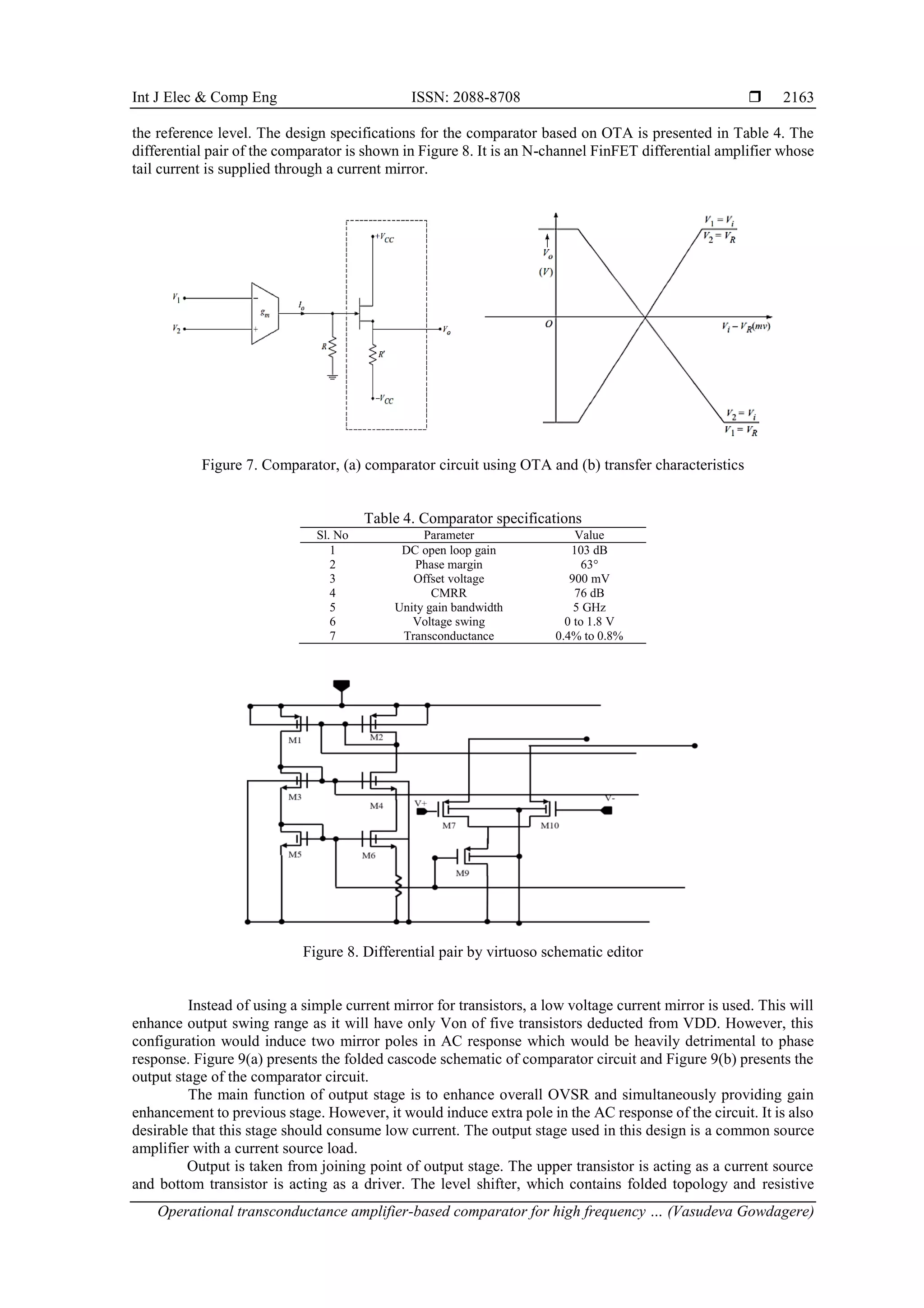
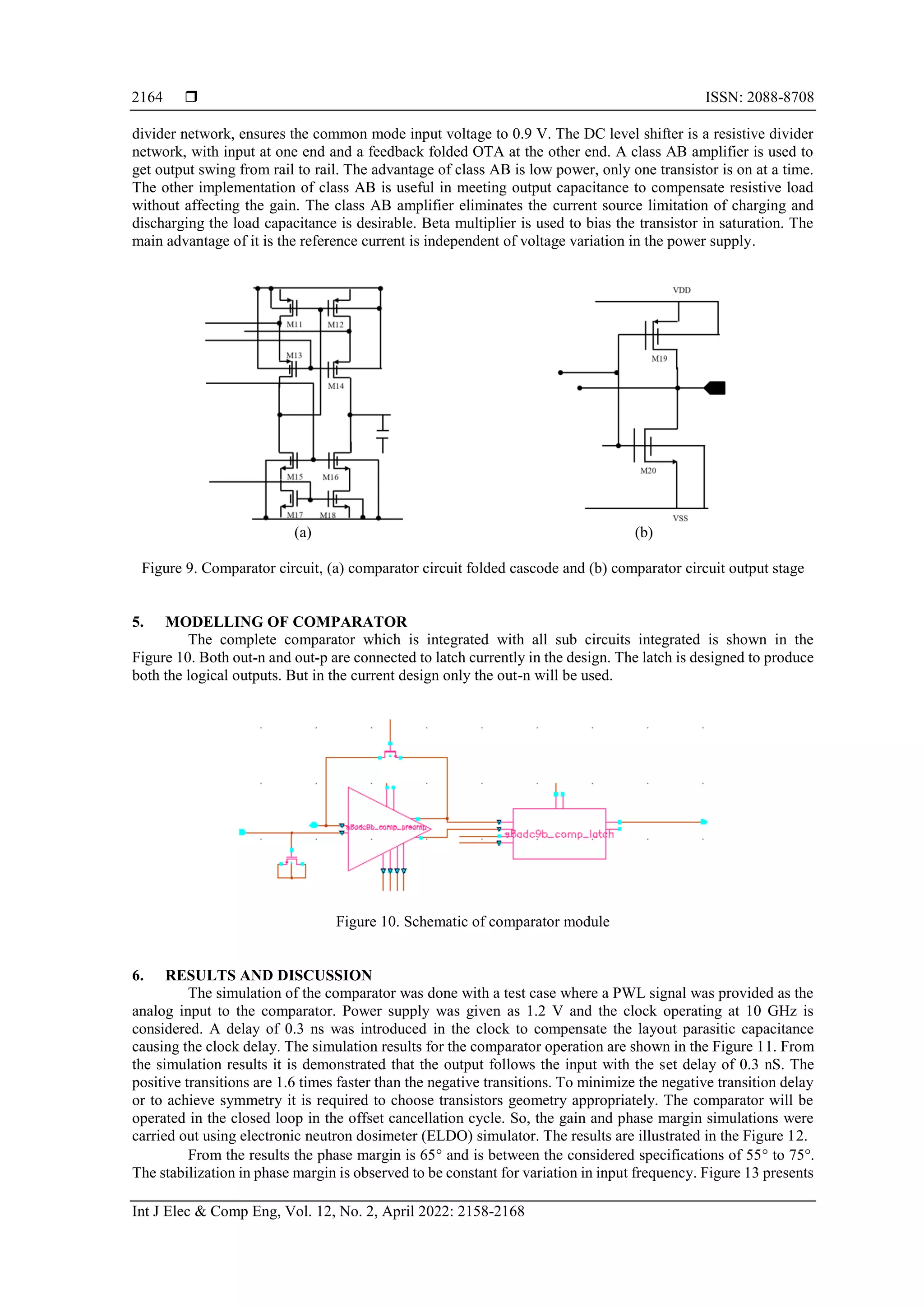
4. OTA BASED COMPARATOR
For an OTA to function as a comparator, it has to be operated in the non-linear region of its
characteristic. The OTA will basically act as a comparator with current output. The circuit for OTA-based
comparator is shown in Figure 7(a). For the proper operation, the output current (or voltage across load) should
be constant value I(1) or V(1) for Vi>VR and another constant value I(0) or V(0) for Vi<VR. The transfer
characteristic is shown in Figure 7(b). The special features of an OTA-based comparator are that the voltages
V0 and V1 may be varied simply by varying the bias current IB or the voltage VB. Because I0 is directly
proportional to IB, the change in IB causes the OTA to saturate at different levels of voltages. Thus, different
levels of output voltages may be obtained through bias current control.
A comparator is a circuit, which compares input signal Vi with a reference voltage VR. Usually, the
reference voltage VR is applied to non-inverting terminal with a proper load and buffer connected at the output,
the OTA behaves like a differential voltage current voltage source. With the buffered OTA, the output voltage
will switch from a positive V1 level to a negative V0 level, as the inverting signal is less than or greater than](https://image.slidesharecdn.com/11125527emr21jul30mark-220628024625-4ed6bfe9/75/Operational-transconductance-amplifier-based-comparator-for-high-frequency-applications-using-22-nm-FinFET-technology-5-2048.jpg)
![Int J Elec & Comp Eng ISSN: 2088-8708
Operational transconductance amplifier-based comparator for high frequency … (Vasudeva Gowdagere)
2167
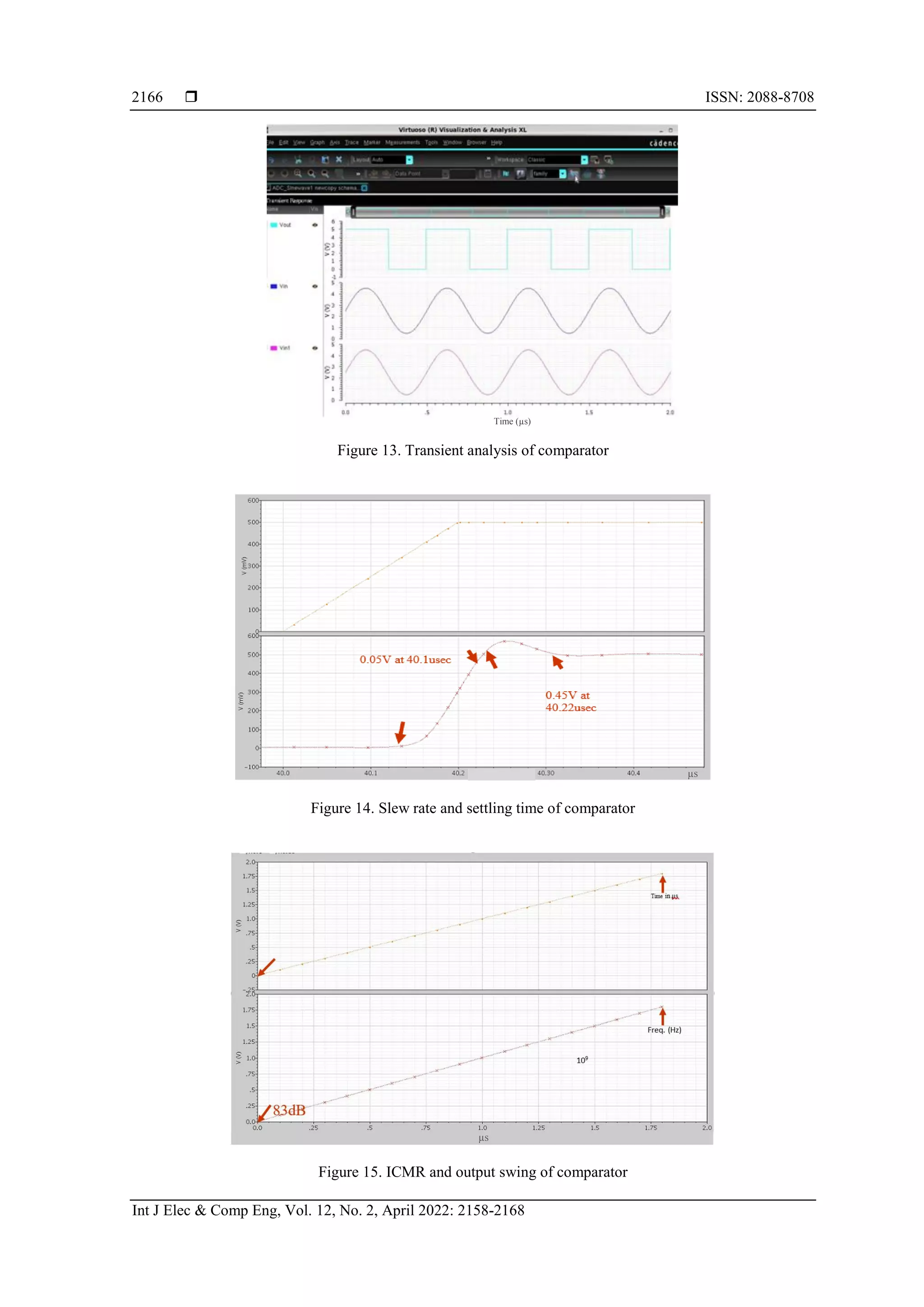
Figure 16. PSRR of comparator
Table 5. Comparison of required specifications and achieved results
Specifications Required Achieved
Gain of the Comparator >100 dB 106 dB
Phase Margin 55° to 75° 65°
CMRR 65 dB to 90 dB 76 dB
Unity Gain Bandwidth >2 GHz 5 GHz
Transconductance 0.4% to 0.8% 0.71%
Technology 22 nm 22 nm
7. CONCLUSION
A new method for achieving constant in a rail-to-rail OTA design is discussed in this work that is
based on one input differential pair and level shifters. The common mode of the OTA is shifted to a constant
value before the signal is input to the differential pair. Since the common-mode level of the differential pair is
fixed, consistent operation for rail-to-rail common-mode inputs is achieved. Furthermore, since only one
differential pair is used, there is no degradation in the CMRR for any input common-mode levels. Simulated
results of this comparator show 0.71% deviation as compared with the desired requirements. The performances
of OTA based comparator is suitable for data converters.
ACKNOWLEDGEMENT
The authors thank RV College of Engineering for providing access to Cadence design suite license
V6.7.11 using which the schematic capture and simulation results were carried out. We acknowledge PTM.edu
for giving us permission to use FinFET model files and access to device parameters for our work. The authors
acknowledge the valuable suggestions given by Prof. Cyril Prasanna Raj P.
REFERENCES
[1] T. Matsukawa et al., “Decomposition of on-current variability of nMOS FinFETs for prediction beyond 20 nm,” IEEE Transactions
on Electron Devices, vol. 59, no. 8, pp. 2003–2010, Aug. 2012, doi: 10.1109/TED.2012.2196766.
[2] M. S. Kim, H. Liu, X. Li, S. Datta, and V. Narayanan, “A steep-slope tunnel FET based SAR analog-to-digital converter,” IEEE
Transactions on Electron Devices, vol. 61, no. 11, pp. 3661–3667, Nov. 2014, doi: 10.1109/TED.2014.2359663.
[3] A. M. Bughio, S. D. Guerrieri, F. Bonani, and G. Ghione, “Physics-based modeling of FinFET RF variability under Shorted- and
Independent-Gates bias,” in 2017 Integrated Nonlinear Microwave and Millimetre-wave Circuits Workshop (INMMiC), Apr. 2017,
pp. 1–4, doi: 10.1109/INMMIC.2017.7927300.
[4] V. B. Rahin and A. B. Rahin, “A low-voltage and low-power two-stage operational amplifier using FinFET transistors,”
International Academic Journal of Science and Engineering, vol. 3, no. 4, pp. 80–95, 2016.
[5] M. Nizamuddin, S. A. Loan, A. R. Alamoud, and S. A. Abbassi, “Design, simulation and comparative analysis of CNT based
cascode operational transconductance amplifiers,” Nanotechnology, vol. 26, no. 39, Art. no. 395201, Oct. 2015, doi: 10.1088/0957-
4484/26/39/395201.
[6] R. S. Kushwah and S. Akashe, “FinFET based tunable analog circuit: design and analysis at 45 nm technology,” Chinese Journal
of Engineering, vol. 2013, pp. 1–8, Oct. 2013, doi: 10.1155/2013/165945.
[7] C.-W. Sohn et al., “Device design guidelines for nanoscale FinFETs in RF/analog applications,” IEEE Electron Device Letters,
vol. 33, no. 9, pp. 1234–1236, Sep. 2012, doi: 10.1109/LED.2012.2204853.
[8] F. Khateb, “Bulk-driven floating-gate and bulk-driven quasi-floating-gate techniques for low-voltage low-power analog circuits
design,” AEU - International Journal of Electronics and Communications, vol. 68, no. 1, pp. 64–72, Jan. 2014, doi:
10.1016/j.aeue.2013.08.019.
Hz](https://image.slidesharecdn.com/11125527emr21jul30mark-220628024625-4ed6bfe9/75/Operational-transconductance-amplifier-based-comparator-for-high-frequency-applications-using-22-nm-FinFET-technology-10-2048.jpg)
![ ISSN: 2088-8708
Int J Elec & Comp Eng, Vol. 12, No. 2, April 2022: 2158-2168
2168
[9] S. Chatterjee, Y. Tsividis, and P. Kinget, “0.5-V analog circuit techniques and their application in OTA and filter design,” IEEE
Journal of Solid-State Circuits, vol. 40, no. 12, pp. 2373–2387, Dec. 2005, doi: 10.1109/JSSC.2005.856280.
[10] L. H. C. Ferreira and S. R. Sonkusale, “A 60-dB gain OTA operating at 0.25-V power supply in 130-nm digital CMOS process,”
IEEE Transactions on Circuits and Systems I: Regular Papers, vol. 61, no. 6, pp. 1609–1617, Jun. 2014, doi:
10.1109/TCSI.2013.2289413.
[11] M. Khaleeq, P. K R, K. Thilagam, and B. Lakshmi, “Design of FinFET based self-biased OTA for low power applications,” SSRN
Electronic Journal, 2019, doi: 10.2139/ssrn.3356294.
[12] C. Garcia-Alberdi, A. J. Lopez-Martin, L. Acosta, L. Acosta, R. G. Carvajal, and J. Ramirez-Angulo, “Class AB CMOS tunable
transconductor,” in 2010 53rd IEEE International Midwest Symposium on Circuits and Systems, Aug. 2010, pp. 596–599, doi:
10.1109/MWSCAS.2010.5548898.
[13] A. N. Mohieldin, E. Sanchez-Sinencio, and J. Silva-Martinez, “A fully balanced pseudo-differential OTA with common-mode
feedforward and inherent common-mode feedback detector,” IEEE Journal of Solid-State Circuits, vol. 38, no. 4, pp. 663–668, Apr.
2003, doi: 10.1109/JSSC.2003.809520.
[14] A. N. Ragheb and H. Kim, “Ultra-low power OTA based on bias recycling and subthreshold operation with phase margin
enhancement,” Microelectronics Journal, vol. 60, pp. 94–101, Feb. 2017, doi: 10.1016/j.mejo.2016.12.007.
[15] L. H. C. Ferreira, T. C. Pimenta, and R. L. Moreno, “An ultra-low-voltage ultra-low-power CMOS miller OTA with rail-to-rail
input/output swing,” IEEE Transactions on Circuits and Systems II: Express Briefs, vol. 54, no. 10, pp. 843–847, Oct. 2007, doi:
10.1109/TCSII.2007.902216.
[16] R. Chawla, F. Adil, G. Serrano, and P. E. Hasler, “Programmable Gm-C filters using floating-gate operational transconductance
amplifiers,” IEEE Transactions on Circuits and Systems I: Regular Papers, vol. 54, no. 3, pp. 481–491, Mar. 2007, doi:
10.1109/TCSI.2006.887473.
[17] O. Abdelfattah, G. W. Roberts, I. Shih, and Y.-C. Shih, “An ultra-low-voltage CMOS process-insensitive self-biased OTA with
rail-to-rail input range,” IEEE Transactions on Circuits and Systems I: Regular Papers, vol. 62, no. 10, pp. 2380–2390, Oct. 2015,
doi: 10.1109/TCSI.2015.2469011.
[18] R. A. Thakker et al., “A novel architecture for improving slew rate in FinFET-based op-amps and OTAs,” Microelectronics Journal,
vol. 42, no. 5, pp. 758–765, May 2011, doi: 10.1016/j.mejo.2011.01.010.
[19] D. M. Monticelli, “A quad CMOS single-supply op amp with rail-to-rail output swing,” IEEE Journal of Solid-State Circuits, vol.
21, no. 6, pp. 1026–1034, Dec. 1986, doi: 10.1109/JSSC.1986.1052645.
[20] S. Oh et al., “A dual-slope capacitance-to-digital converter integrated in an implantable pressure-sensing system,” IEEE Journal of
Solid-State Circuits, vol. 50, no. 7, pp. 1581–1591, Jul. 2015, doi: 10.1109/JSSC.2015.2435736.
[21] M. Nizamuddin and D. Sharma, “FinFET based operational transconductance amplifier for low power applications,” International
Journal of Computer Sciences and Engineering, vol. 7, no. 5, pp. 578–581, May 2019, doi: 10.26438/ijcse/v7i5.578581.
[22] A. Amara and O. Rozeau, Eds., Planar double-gate Transistor. Dordrecht: Springer Netherlands, 2009.
[23] F. You, S. H. K. Embabi, and E. Sanchez-Sinencio, “Low-voltage class AB buffers with quiescent current control,” IEEE Journal
of Solid-State Circuits, vol. 33, no. 6, pp. 915–920, Jun. 1998, doi: 10.1109/4.678659.
[24] M. N. Sabry, H. Omran, and M. Dessouky, “Systematic design and optimization of operational transconductance amplifier using
gm/ID design methodology,” Microelectronics Journal, vol. 75, pp. 87–96, May 2018, doi: 10.1016/j.mejo.2018.02.002.
[25] B. Razavi, Design of analog CMOS integrated circuits. 2nd Edition McGraw-Hill Education, 2017.
BIOGRAPHIES OF AUTHORS
Vasudeva Gowdagere is Presently Pursuing Ph.D. in the field of ADC using
FinFETs for low power applications in Electronics and Communication Engineering
Department at RV College of Engineering, Bangalore, affiliated to VTU, Belgaum. He can
be contacted at email: devan.vasu921@gmail.com.
Uma Bidikinamane Venkataramanaiah Currently working as Professor in
ECE Department and Dean Student Affairs at RVCE Bangalore. She has around 27 years
of teaching experience and reserach interests include Broad band Communication, VLSI
design, Microcontroller. She can be contacted at email: umabv@rvce.edu.in.](https://image.slidesharecdn.com/11125527emr21jul30mark-220628024625-4ed6bfe9/75/Operational-transconductance-amplifier-based-comparator-for-high-frequency-applications-using-22-nm-FinFET-technology-11-2048.jpg)