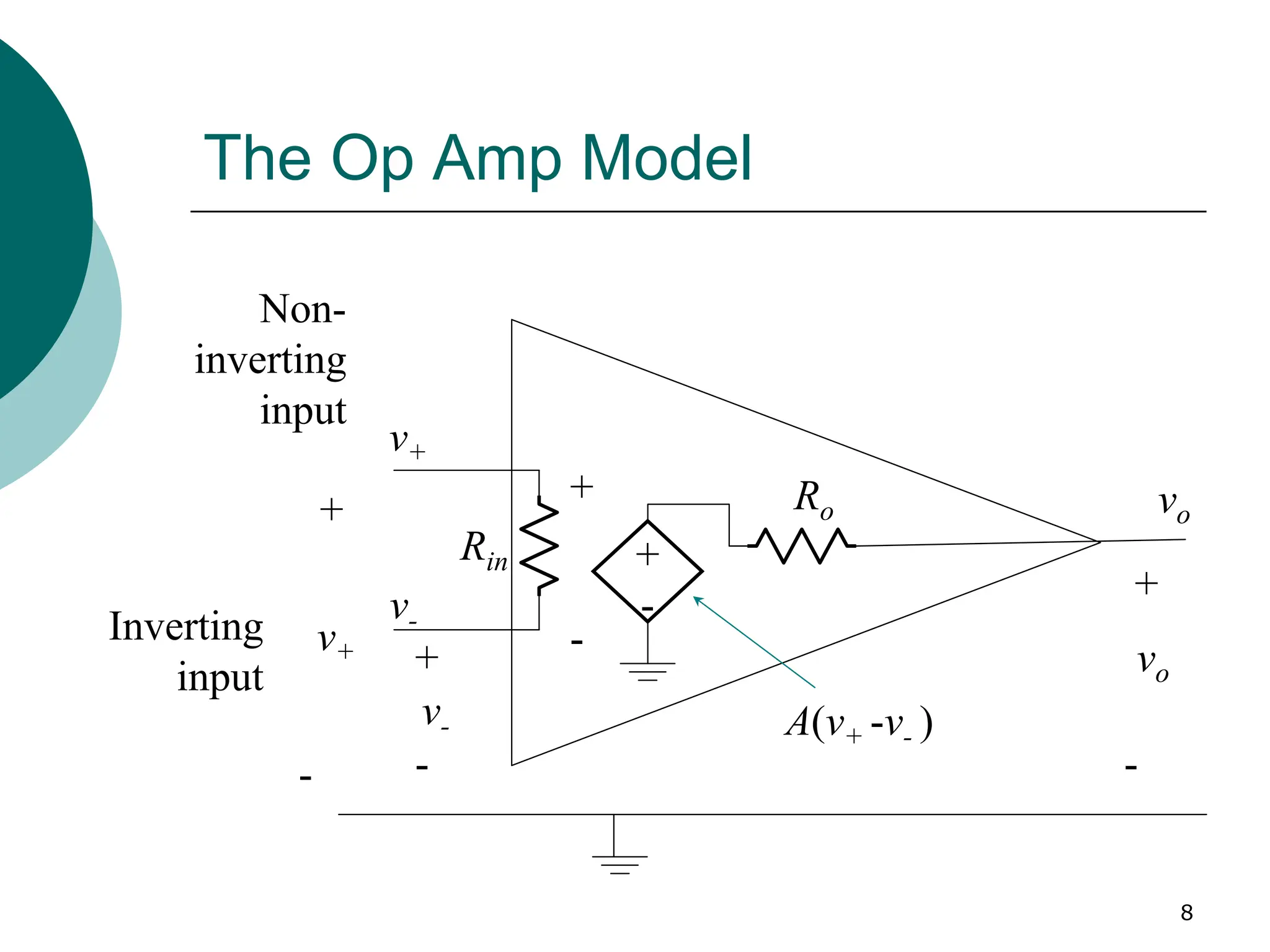
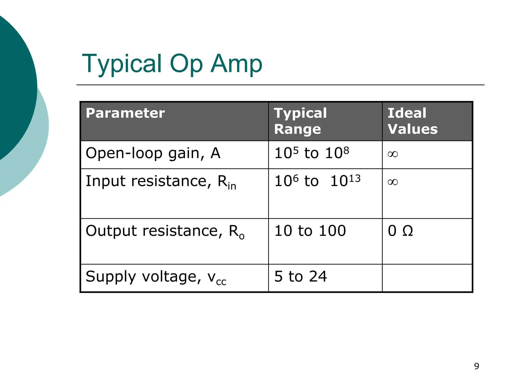
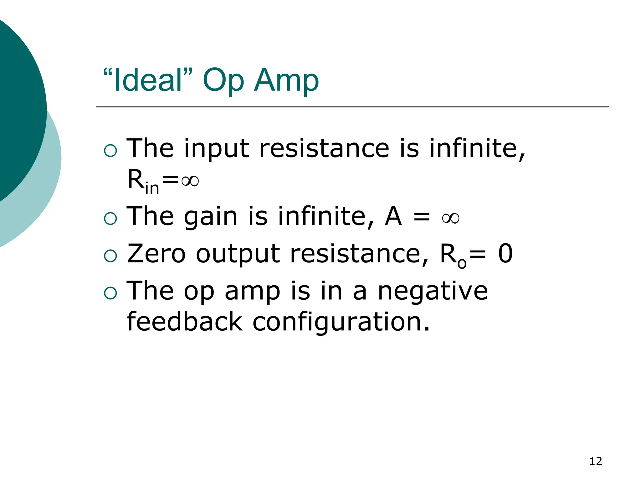
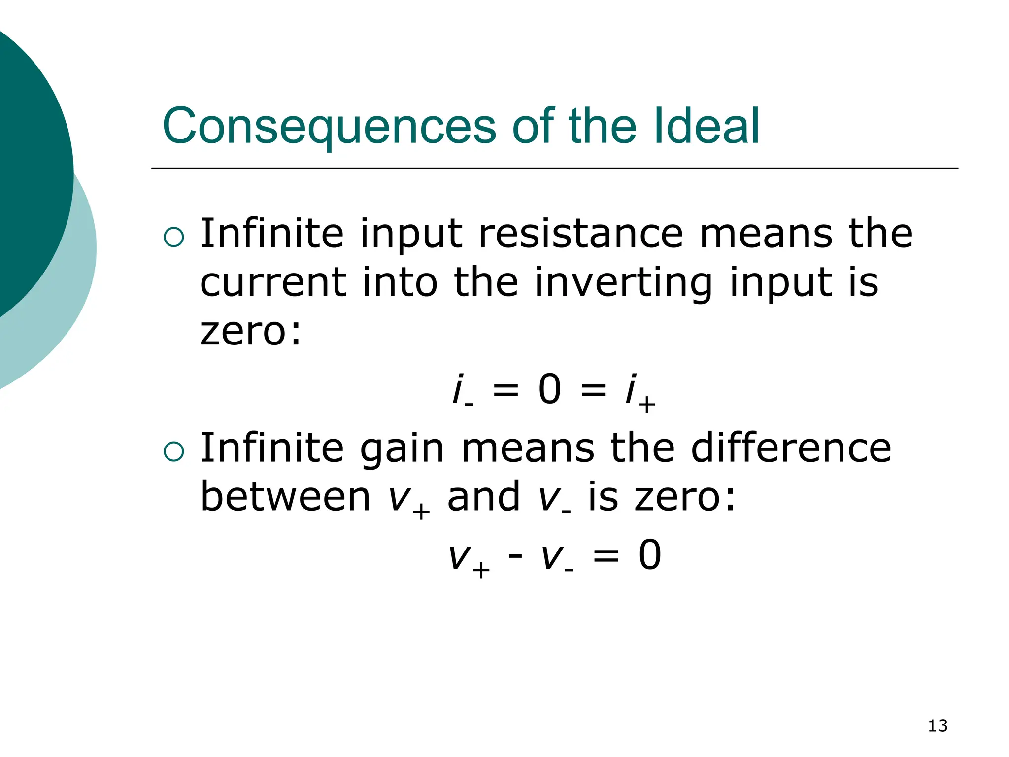
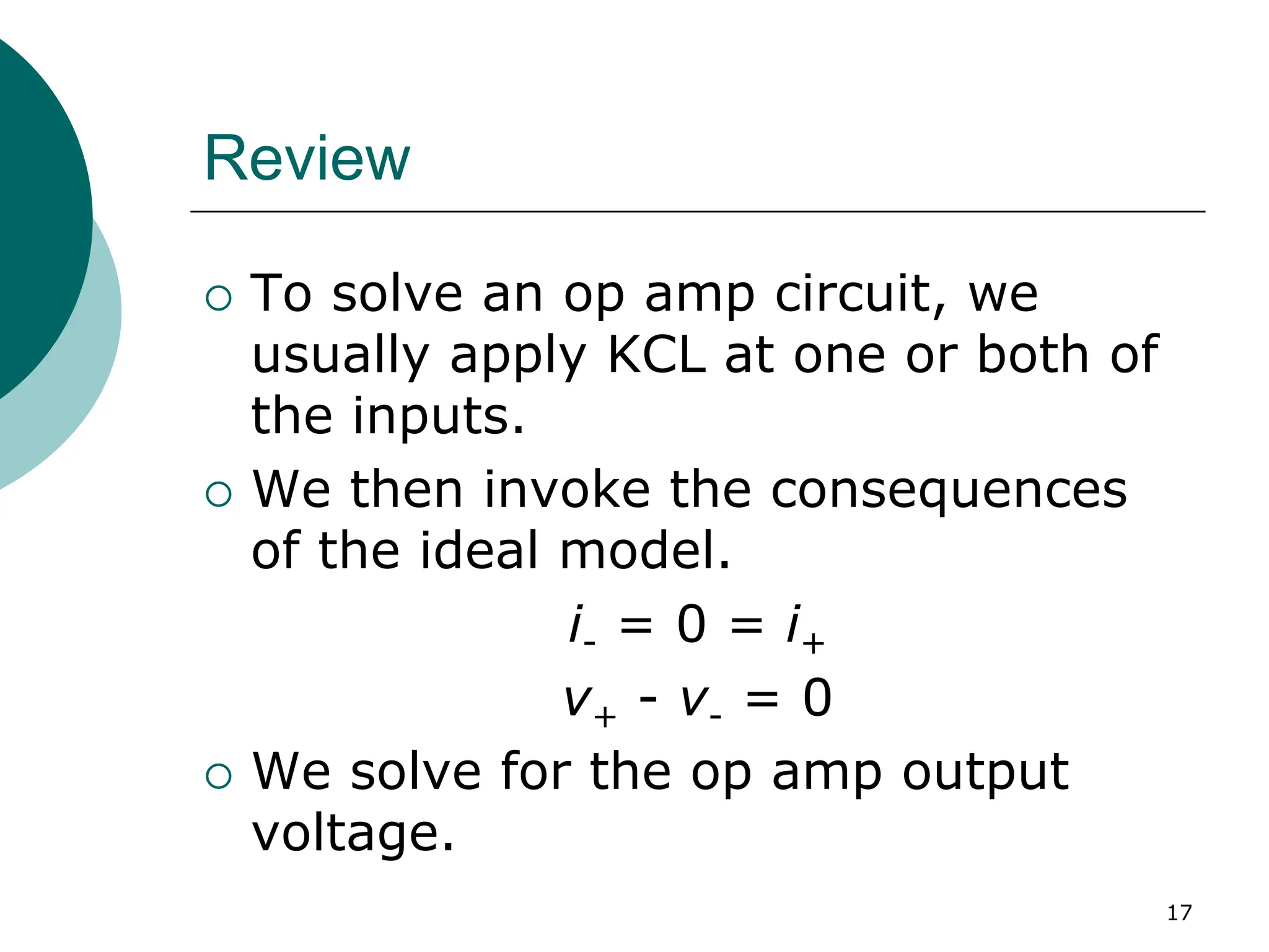
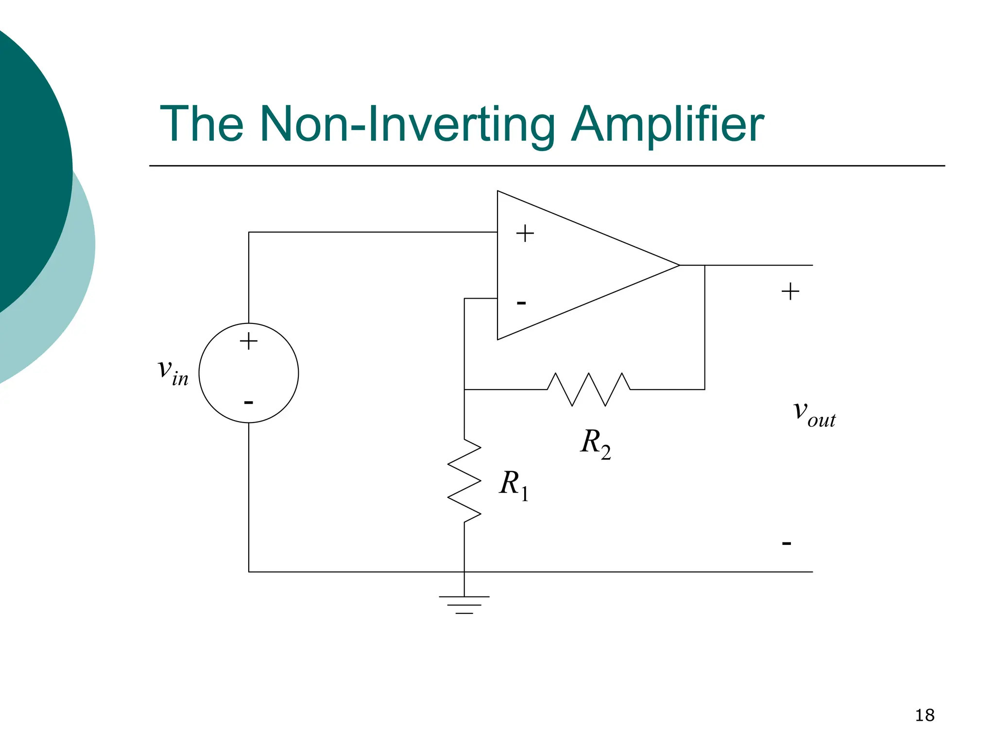
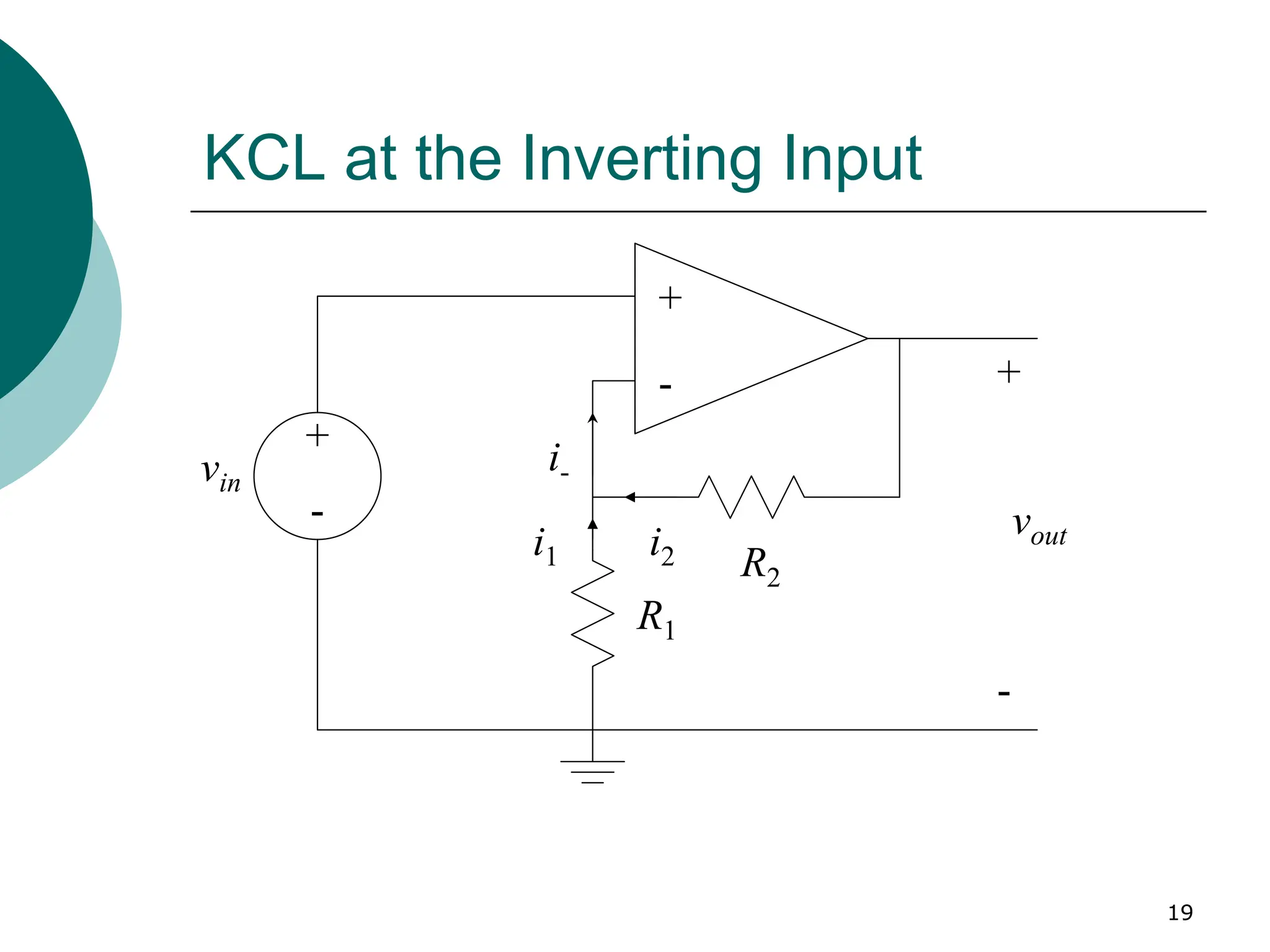
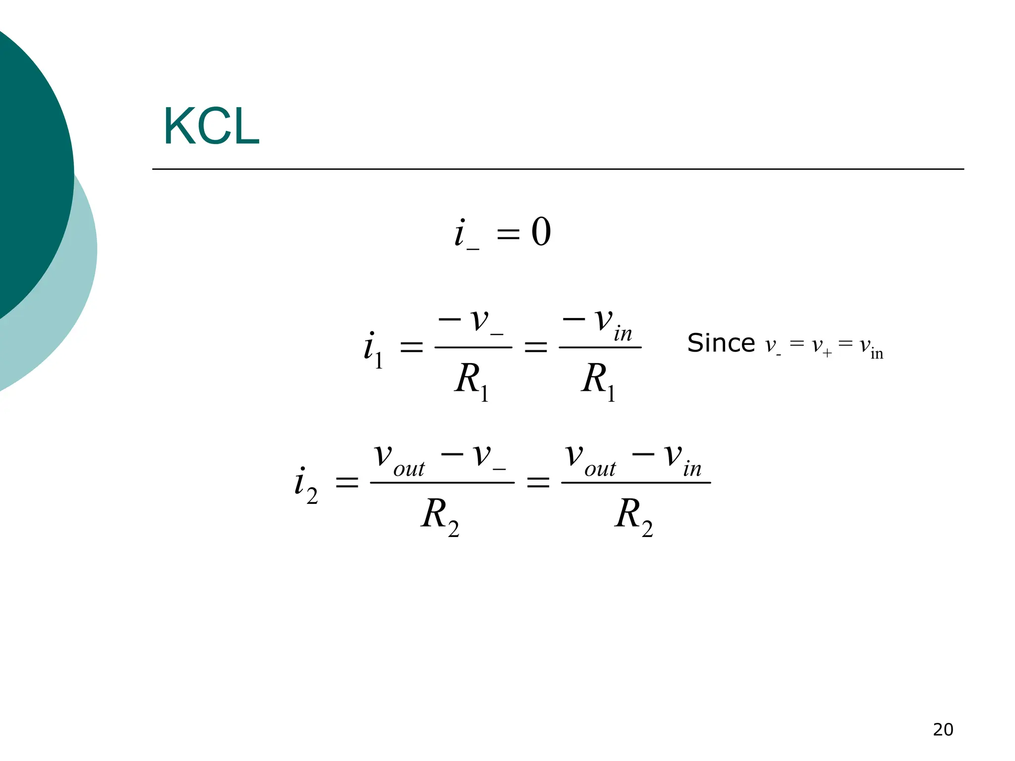
1
Operational Amplifiers
(Op Amps)
Dr. Mustafa Kemal Uyguroğlu
2
Introduction
{ Op Amp is short for operational
amplifier.
{ An operational amplifier is modeled
as a voltage controlled voltage
source.
{ An operational amplifier has a very
high input impedance and a very
high gain.
3
Use of Op Amps
{ Op amps can be configured in many
different ways using resistors and
other components.
{ Most configurations use feedback.
4
Applications of Op Amps
{ Amplifiers provide gains in voltage
or current.
{ Op amps can convert current to
voltage.
{ Op amps can provide a buffer
between two circuits.
{ Op amps can be used to implement
integrators and differentiators.
5
More Applications
{ Lowpass and bandpass filters.
6
The Op Amp Symbol
7
Schematic diagram of op amp
8
The Op Amp Model
+
-
Inverting
input
Non-
inverting
input
Rin
v+
v-
+
-
A(v+ -v- )
vo
Ro
+
-
v-
+
+
-
-
v+ vo
9
Typical Op Amp
5 to 24
Supply voltage, vcc
0 Ω
10 to 100
Output resistance, Ro
∞
106 to 1013
Input resistance, Rin
∞
105 to 108
Open-loop gain, A
Ideal
Values
Typical
Range
Parameter
10
Example
{ A 741 op amp has an open-loop voltage gain of 2 x 10⁵, input
resistance of 2 MΩ, and output resistance of 50 Ω.The op amp is
used in the circuit shown below. Find the closed- loop gain v0/vs. Find i0
when vs = 1 V.
+
-
5 kΩ
vs
40 kΩ
io
20 kΩ vo
+
-
+
-
+
-
vs
2 MΩvin 2 ×10
5
vin
50 Ω io
40 kΩ
5 kΩ 20 kΩ vo
Equivalent circuit
11
Example cont.
io
+
-
+
-
vs
2 MΩ
vin
5 kΩ
v1
40 kΩ
2 ×10
5
vin
50 Ω
vo
20 kΩ
1 1 0
1
6 3 3
0
2 10 5 10 40 10
s
v v v v
v
− −
+ + =
× × ×
•Redrawn for clarity
KCL at v1
KCL at v0
5
0 0 1 0 1
3 3
2 10 ( )
0
20 10 40 10 50
s
v v v v v v
− − × −
+ + =
× ×
v0 = 9.0004vs
i0 = 0.675 mA
12
“Ideal” Op Amp
{ The input resistance is infinite,
Rin=∞
{ The gain is infinite, A = ∞
{ Zero output resistance, Ro= 0
{ The op amp is in a negative
feedback configuration.
13
Consequences of the Ideal
{ Infinite input resistance means the
current into the inverting input is
zero:
i- = 0 = i+
{ Infinite gain means the difference
between v+ and v- is zero:
v+ - v- = 0
14
Example
vo
io
+
-
i- = 0
i+ = 0
vs
vs
vs
40 kΩ
5 kΩ 20 kΩ
vo
0
0
0
40 5
9
s s
s
v v v
v v
−
+ =
=
KCL at noninverting
terminal:
If vs = 1 V then i0 = 0.65 mA
0 0
0
20 40
s
v v v
i
k k
−
 
= +
 
 
KCL at v0:
15
Inverting Amplifier
1 2 0
v v
= =
0
1 2
1
0 0
i
f
v v
i i
R R
− −
= ⇒ =
Since the noninverting terminal is grounded
KCL at v1:
0
1
f
i
R
v v
R
= −
16
Where is the Feedback?
-
+
Vin
+
-
+
-
Vout
R1
R2
17
Review
{ To solve an op amp circuit, we
usually apply KCL at one or both of
the inputs.
{ We then invoke the consequences
of the ideal model.
i- = 0 = i+
v+ - v- = 0
{ We solve for the op amp output
voltage.
18
The Non-Inverting Amplifier
+
-
vin
+
-
+
-
vout
R1
R2
19
KCL at the Inverting Input
+
-
vin
+
-
+
-
vout
R1
R2
i-
i1 i2
20
KCL
0
=
−
i
1
1
1
R
v
R
v
i in
−
=
−
= −
2
2
2
R
v
v
R
v
v
i in
out
out −
=
−
= −
Since v- = v+ = vin
21
Solve for Vout
0
2
1
=
−
+
−
R
v
v
R
v in
out
in








+
=
1
2
1
R
R
v
v in
out
22
The Voltage Follower
23
Inverting Summer
_ = 0
24
KCL at the Inverting Input
-
+
v2
+
-
+
-
vout
R2
Rf
R1
v1
+
-
i1
i3
if
i-
v3
+
-
R3
i2
25
KCL
since 0
v− =
1
1
1
1
1
R
v
R
v
v
i =
−
= −
2
2
2
2
2
R
v
R
v
v
i =
−
= −
3 3
3
3 3
v v v
i
R R
−
−
= =
26
KCL
0
=
−
i
f
out
f
out
f
R
v
R
v
v
i =
−
= −
27
Solve for Vout
3
1 2
1 2 3
0
out
f
v v
v v
R R R R
+ + + =
1 2 3
1 2 3
f f f
out
R R R
v v v v
R R R
= − − −
28
Noninverting Summer
+
-
v2
+
-
+
-
vout
R2
Ra
R1
v1
+
-
i1
i3
ia
i-
v3
+
-
R3
i2
Rf
if
29
1 2 3
1
1
1
0
i i i
v v
i
R
+
+ + =
−
=
2
2
2
v v
i
R
+
−
=
3
3
3
v v
i
R
+
−
=
KCL at noninverting input: KCL at inverting input:
0
f a
out
f
f
i i
v v
i
R
−
+ =
−
=
a
a
a
out
a f
v
i
R
R
v v
R R
v v
−
−
− +
=
=
+
=
30
1 2 3
3
1 2
1 2 3 1 2 3
1 2 3
3
1 2
1 2 3
0
1 1 1
1 1 1 1
1
T
a
out
T a f
i i i
v
v v
v
R R R R R R
R R R R
v R
v v
v
R R R R R R
+
+ + =
 
+ + = + +
 
 
 
= + +
 
 
+ + =
+
1 2 3
1 2 3
1
f T T T
out
a
R R R R
v v v v
R R R R
  
= + + +
  
  
31
The difference amplifier
32
2
3 4
4
2
3 4
KCL at node :
b
b b
b a
v
v v v
R R
R
v v v
R R
−
=
= =
+
33
1
1 2
1
2 1 2 1
2 2 2 4 2
1 2 1
1 1 1 3 4 1
1
2
2 2 2 2
0 2 1 2 1
3 3
1 1 1 1
4 4
KCL at
0
1 1 1 1
1 1
1
1
1
1 1
a
a a o
o a
o a
v
v v v v
R R
v v v
R R R R
R R R R R
v v v v v
R R R R R R
R
R
R R R R
v v v v v
R R
R R R R
R R
− −
+ =
 
= + −
 
 
   
= + − = + −
   
+
   
 
+
 
   
= + − = −
 
  + +
34
{ Since a difference must reject a signal common
to the two inputs, the amplifier must have the
property that v0 = 0 when v1 = v2. This implies
that
4
3
2
1
R
R
R
R
=
When R1 = R2 and R3 = R4 it acts like a subtractor
1
2 v
v
vo −
=
35
Interconnecting of Op Amps
36
Example
+
+
+
- - -
v1 v2
v3
10 kΩ
10 kΩ
40 kΩ
20 kΩ
20 kΩ
50 kΩ
25 kΩ
25 kΩ
12 V
Find the voltage transfer equation of the following circuit

op amp presentation electronic circuit design

  • 1.
  • 2.
    2 Introduction { Op Ampis short for operational amplifier. { An operational amplifier is modeled as a voltage controlled voltage source. { An operational amplifier has a very high input impedance and a very high gain.
  • 3.
    3 Use of OpAmps { Op amps can be configured in many different ways using resistors and other components. { Most configurations use feedback.
  • 4.
    4 Applications of OpAmps { Amplifiers provide gains in voltage or current. { Op amps can convert current to voltage. { Op amps can provide a buffer between two circuits. { Op amps can be used to implement integrators and differentiators.
  • 5.
    5 More Applications { Lowpassand bandpass filters.
  • 6.
  • 7.
  • 8.
    8 The Op AmpModel + - Inverting input Non- inverting input Rin v+ v- + - A(v+ -v- ) vo Ro + - v- + + - - v+ vo
  • 9.
    9 Typical Op Amp 5to 24 Supply voltage, vcc 0 Ω 10 to 100 Output resistance, Ro ∞ 106 to 1013 Input resistance, Rin ∞ 105 to 108 Open-loop gain, A Ideal Values Typical Range Parameter
  • 10.
    10 Example { A 741op amp has an open-loop voltage gain of 2 x 10⁵, input resistance of 2 MΩ, and output resistance of 50 Ω.The op amp is used in the circuit shown below. Find the closed- loop gain v0/vs. Find i0 when vs = 1 V. + - 5 kΩ vs 40 kΩ io 20 kΩ vo + - + - + - vs 2 MΩvin 2 ×10 5 vin 50 Ω io 40 kΩ 5 kΩ 20 kΩ vo Equivalent circuit
  • 11.
    11 Example cont. io + - + - vs 2 MΩ vin 5kΩ v1 40 kΩ 2 ×10 5 vin 50 Ω vo 20 kΩ 1 1 0 1 6 3 3 0 2 10 5 10 40 10 s v v v v v − − + + = × × × •Redrawn for clarity KCL at v1 KCL at v0 5 0 0 1 0 1 3 3 2 10 ( ) 0 20 10 40 10 50 s v v v v v v − − × − + + = × × v0 = 9.0004vs i0 = 0.675 mA
  • 12.
    12 “Ideal” Op Amp {The input resistance is infinite, Rin=∞ { The gain is infinite, A = ∞ { Zero output resistance, Ro= 0 { The op amp is in a negative feedback configuration.
  • 13.
    13 Consequences of theIdeal { Infinite input resistance means the current into the inverting input is zero: i- = 0 = i+ { Infinite gain means the difference between v+ and v- is zero: v+ - v- = 0
  • 14.
    14 Example vo io + - i- = 0 i+= 0 vs vs vs 40 kΩ 5 kΩ 20 kΩ vo 0 0 0 40 5 9 s s s v v v v v − + = = KCL at noninverting terminal: If vs = 1 V then i0 = 0.65 mA 0 0 0 20 40 s v v v i k k −   = +     KCL at v0:
  • 15.
    15 Inverting Amplifier 1 20 v v = = 0 1 2 1 0 0 i f v v i i R R − − = ⇒ = Since the noninverting terminal is grounded KCL at v1: 0 1 f i R v v R = −
  • 16.
    16 Where is theFeedback? - + Vin + - + - Vout R1 R2
  • 17.
    17 Review { To solvean op amp circuit, we usually apply KCL at one or both of the inputs. { We then invoke the consequences of the ideal model. i- = 0 = i+ v+ - v- = 0 { We solve for the op amp output voltage.
  • 18.
  • 19.
    19 KCL at theInverting Input + - vin + - + - vout R1 R2 i- i1 i2
  • 20.
  • 21.
    21 Solve for Vout 0 2 1 = − + − R v v R vin out in         + = 1 2 1 R R v v in out
  • 22.
  • 23.
  • 24.
    24 KCL at theInverting Input - + v2 + - + - vout R2 Rf R1 v1 + - i1 i3 if i- v3 + - R3 i2
  • 25.
    25 KCL since 0 v− = 1 1 1 1 1 R v R v v i= − = − 2 2 2 2 2 R v R v v i = − = − 3 3 3 3 3 v v v i R R − − = =
  • 26.
  • 27.
    27 Solve for Vout 3 12 1 2 3 0 out f v v v v R R R R + + + = 1 2 3 1 2 3 f f f out R R R v v v v R R R = − − −
  • 28.
  • 29.
    29 1 2 3 1 1 1 0 ii i v v i R + + + = − = 2 2 2 v v i R + − = 3 3 3 v v i R + − = KCL at noninverting input: KCL at inverting input: 0 f a out f f i i v v i R − + = − = a a a out a f v i R R v v R R v v − − − + = = + =
  • 30.
    30 1 2 3 3 12 1 2 3 1 2 3 1 2 3 3 1 2 1 2 3 0 1 1 1 1 1 1 1 1 T a out T a f i i i v v v v R R R R R R R R R R v R v v v R R R R R R + + + =   + + = + +       = + +     + + = + 1 2 3 1 2 3 1 f T T T out a R R R R v v v v R R R R    = + + +      
  • 31.
  • 32.
    32 2 3 4 4 2 3 4 KCLat node : b b b b a v v v v R R R v v v R R − = = = +
  • 33.
    33 1 1 2 1 2 12 1 2 2 2 4 2 1 2 1 1 1 1 3 4 1 1 2 2 2 2 2 0 2 1 2 1 3 3 1 1 1 1 4 4 KCL at 0 1 1 1 1 1 1 1 1 1 1 1 a a a o o a o a v v v v v R R v v v R R R R R R R R R v v v v v R R R R R R R R R R R R v v v v v R R R R R R R R − − + =   = + −         = + − = + −     +       +       = + − = −     + +
  • 34.
    34 { Since adifference must reject a signal common to the two inputs, the amplifier must have the property that v0 = 0 when v1 = v2. This implies that 4 3 2 1 R R R R = When R1 = R2 and R3 = R4 it acts like a subtractor 1 2 v v vo − =
  • 35.
  • 36.
    36 Example + + + - - - v1v2 v3 10 kΩ 10 kΩ 40 kΩ 20 kΩ 20 kΩ 50 kΩ 25 kΩ 25 kΩ 12 V Find the voltage transfer equation of the following circuit