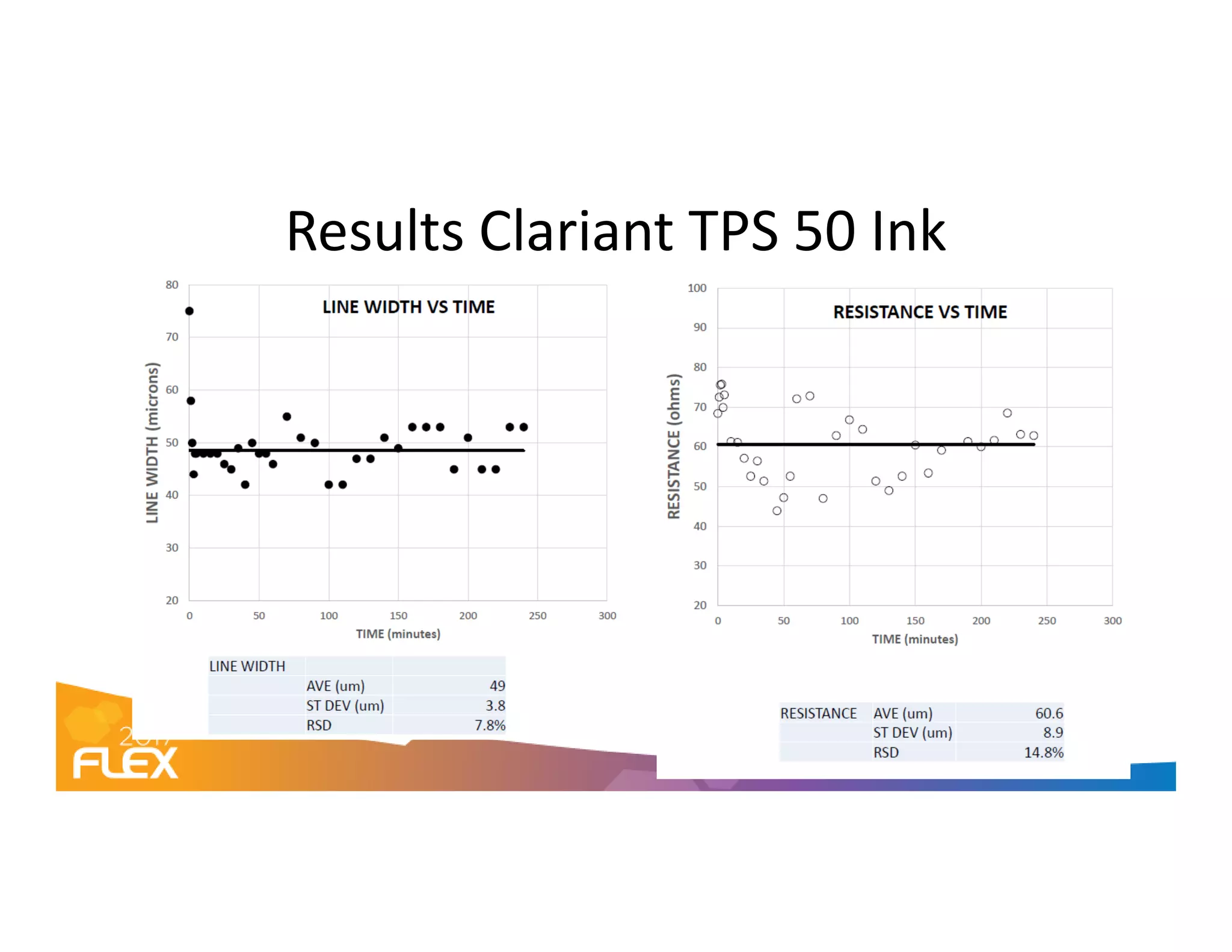
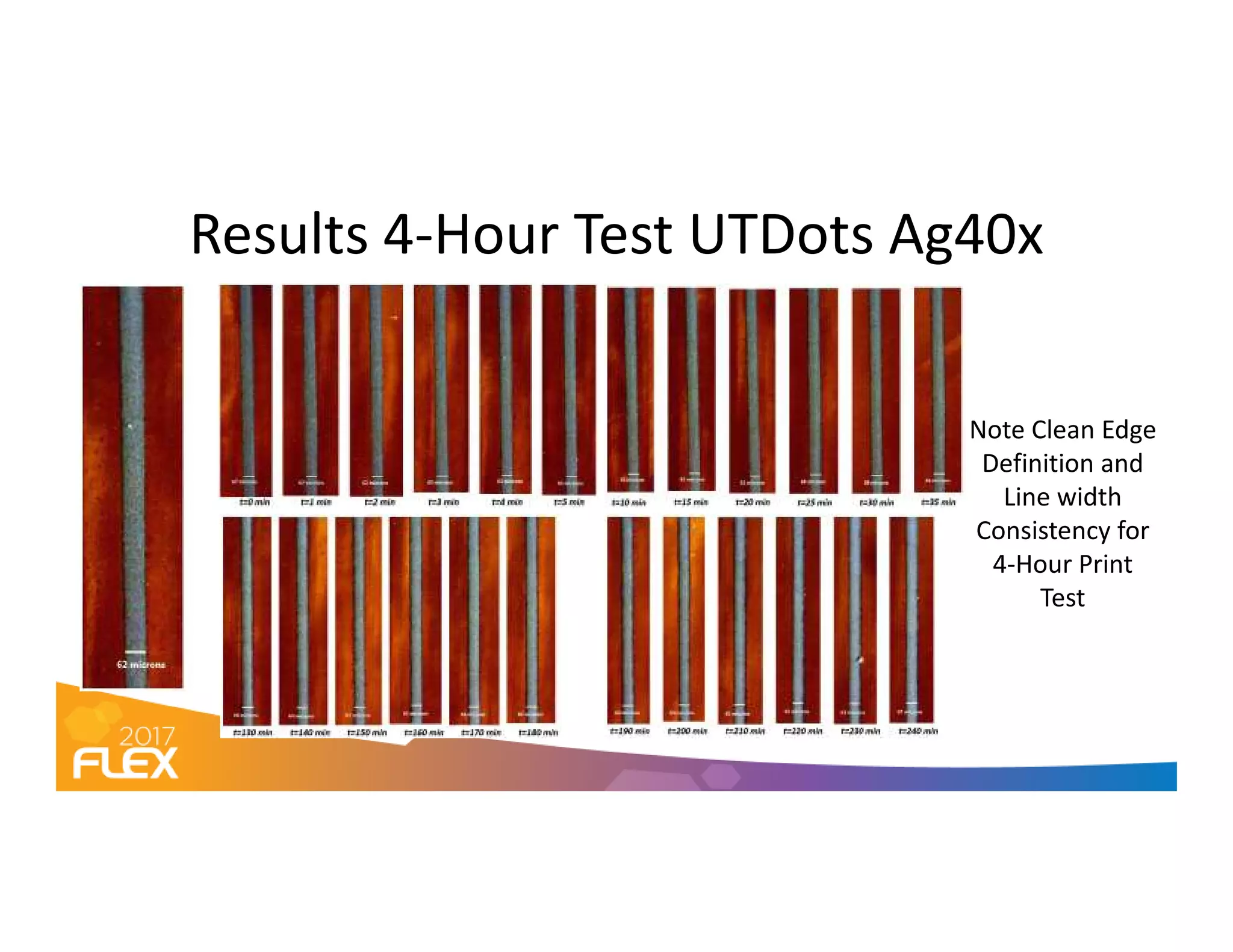
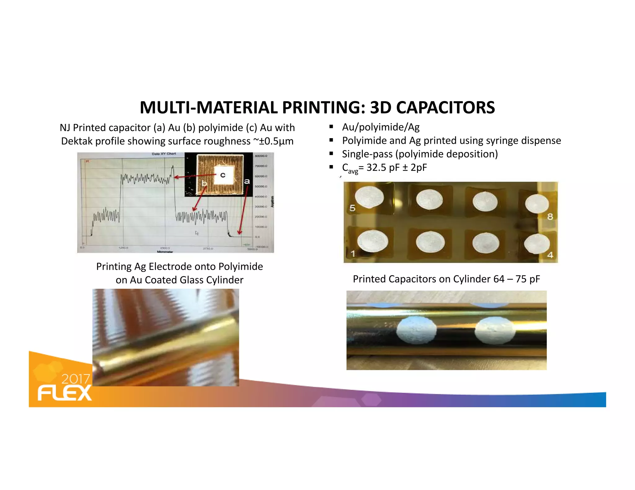
Next Generation Aerosol-Based
Printing for Production-LevelPrinting for Production-Level
Printed Electronics
D. Keicher1, M. Essien2, J. Lavin1, S. Whetten1, S. Mani1
1 - Sandia National Laboratories
2 – Integrated Deposition Solutions
Introduction
• Background
• Development Goals
• Print Head
• Print Process Results
– Run time testing– Run time testing
– Conductors
– Capacitors
• Conclusions
• Future Development
Background
• Key Personnel
– Inventor of AJ Technology
– Other AM Technology
– Technical Staff and Student Interns
• Significant Experience with AJ Printing• Significant Experience with AJ Printing
– Strengths
– Weaknesses
• Leverage Sandia Technology for Improvements
– Brockman, et.al. Patent, September 1999
Development Goals
• Focus on User Experience with Printing
– Consistent print performance
– Ease of use
– Reliable
– Quick material change over
– Remove “Art” from operation– Remove “Art” from operation
• Production Oriented Solution
– MTBA > 4 hours
– Print quality
• Well defined print edges
• <5% variation for key parameters during print
– Cost of ownership
Multiple Aerodynamic Lens Aerosol Focusing
• Poly dispersed particle source
– Droplets range from 200 nm to 3-5µm.
– Multiple Aerodynamic Lenses
• Optimal focusing of all droplets sizes
• Highly collimated print stream
– Minimizes overspray/satellites of smaller droplet sizes
2nd Lens Focuses Smaller Droplets Coaxial with
Larger Droplets, Creates Highly Collimated
Aerosol Stream
Multiple Aerodynamic Lenses Enhance Focusing for Polydispersed Aerosol
Next Generation NanoJet™ Print Head Operation
Cartridge Based Prototype
Print Head Generation 4
1.6 cm
Print Process Results 4 Hour Run Testing
• Inks
– Clariant Preselect TPS 50
– UTDots Ag 40 silver np inks
• Substrate
– Poylimide
• Configuration• Configuration
– New Cartridge Installation and Testing
• Analysis
– Optical measurements of printed linewidth
– Resistivity measurement
• Target Line width: ~ 60 microns
• Test Duration – 4 hours
Results 4-Hour Test Clariant TPS 50 Ink
Note Edge
Definition and
Line width
Consistency
for 4-Hour
Print Test
Results Clariant TPS 50 Ink
Results 4-Hour Test UTDots Ag40x
Note Clean Edge
Definition andDefinition and
Line width
Consistency for
4-Hour Print
Test
Results UTDots Ag40X
SINGLE PASS LINE HEIGHT MEASUREMENTS
v=2 mm/s
Line height varies from ~4 to 1 micron/pass for print speeds from 2 to 10 mm/s.
0.5
1
1.5
2
2.5
3
3.5
4
Height(µµµµm)
v=20 mm/s
13
0.5
0 2 4 6 8 10 12
Velocity (mm/s)
MULTI-MATERIAL PRINTING: 3D CAPACITORS
NJ Printed capacitor (a) Au (b) polyimide (c) Au with
Dektak profile showing surface roughness ~±0.5µm
Au/polyimide/Ag
Polyimide and Ag printed using syringe dispense
Single-pass (polyimide deposition)
Cavg= 32.5 pF ± 2pF
AB
Printing Ag Electrode onto Polyimide
on Au Coated Glass Cylinder Printed Capacitors on Cylinder 64 – 75 pF
Printed Resistors on Glass Slide
EXPERIMENTAL
• UTDAg40X (0.2ml) Terpeniol (20 drops)
• 200 micron tip
• Sintered at 200C for 90 minutes
• Sintered 50C for 60 minutes
RESULTSRESULTS
• Lines measured ~60 microns x 20mm
• Resistance = 2 kohm consistently
• Lines adhered extremely well to surface
after sintering. Rubbing with isopropyl
alcohol did not remove any material
• No overspray observed
Conclusions
• Accomplished Goals and Objectives of Effort
• Developed and Demonstrated Robust Aerosol
Print SolutionPrint Solution
• Working with Internal Customers to
Demonstrate Applications
Future Work
• Test Printing to Failure
• Large Area Printing
• Multi Nozzle Printing
• Multi Material Printing• Multi Material Printing
• Work with Internal and External Customers to
Apply Technology
Printed Dielectric Film Properties
Cross-sectional view of STA spray UTDPI sample, showing surface
roughness and overspray of polymer on the film surface
Group N Weibull α (kV/cm) Weibull β
AM spray UTD PI 69 2402 1.5
solvent cast UTD PI 54 2060 1.0
Dielectric breakdown strength
Printed film thickness
Group N*
avg. thickness
(μm)
κ Df
AM spray UTD PI 81 6.6 (1.8) 3.05 (0.77) 0.0021 (0.0005)
commercial 90 13.3 (0.2) 3.25 (0.02) 0.0021 (0.0004)
solvent cast UTD PI 31 2.6 (0.9) 3.25 (0.64) 0.0036 (0.0005)
solvent cast UTD PI 54 2060 1.0
commercial 89 4891 13.0
Permittivity and Dielectric Loss Mean (St. Dev)

Next generation aerosol-based printing for production-level printed electronics

  • 1.
    Next Generation Aerosol-Based Printingfor Production-LevelPrinting for Production-Level Printed Electronics D. Keicher1, M. Essien2, J. Lavin1, S. Whetten1, S. Mani1 1 - Sandia National Laboratories 2 – Integrated Deposition Solutions
  • 2.
    Introduction • Background • DevelopmentGoals • Print Head • Print Process Results – Run time testing– Run time testing – Conductors – Capacitors • Conclusions • Future Development
  • 3.
    Background • Key Personnel –Inventor of AJ Technology – Other AM Technology – Technical Staff and Student Interns • Significant Experience with AJ Printing• Significant Experience with AJ Printing – Strengths – Weaknesses • Leverage Sandia Technology for Improvements – Brockman, et.al. Patent, September 1999
  • 4.
    Development Goals • Focuson User Experience with Printing – Consistent print performance – Ease of use – Reliable – Quick material change over – Remove “Art” from operation– Remove “Art” from operation • Production Oriented Solution – MTBA > 4 hours – Print quality • Well defined print edges • <5% variation for key parameters during print – Cost of ownership
  • 5.
    Multiple Aerodynamic LensAerosol Focusing • Poly dispersed particle source – Droplets range from 200 nm to 3-5µm. – Multiple Aerodynamic Lenses • Optimal focusing of all droplets sizes • Highly collimated print stream – Minimizes overspray/satellites of smaller droplet sizes 2nd Lens Focuses Smaller Droplets Coaxial with Larger Droplets, Creates Highly Collimated Aerosol Stream Multiple Aerodynamic Lenses Enhance Focusing for Polydispersed Aerosol
  • 6.
    Next Generation NanoJet™Print Head Operation Cartridge Based Prototype Print Head Generation 4 1.6 cm
  • 7.
    Print Process Results4 Hour Run Testing • Inks – Clariant Preselect TPS 50 – UTDots Ag 40 silver np inks • Substrate – Poylimide • Configuration• Configuration – New Cartridge Installation and Testing • Analysis – Optical measurements of printed linewidth – Resistivity measurement • Target Line width: ~ 60 microns • Test Duration – 4 hours
  • 8.
    Results 4-Hour TestClariant TPS 50 Ink Note Edge Definition and Line width Consistency for 4-Hour Print Test
  • 9.
  • 10.
    Results 4-Hour TestUTDots Ag40x Note Clean Edge Definition andDefinition and Line width Consistency for 4-Hour Print Test
  • 11.
  • 13.
    SINGLE PASS LINEHEIGHT MEASUREMENTS v=2 mm/s Line height varies from ~4 to 1 micron/pass for print speeds from 2 to 10 mm/s. 0.5 1 1.5 2 2.5 3 3.5 4 Height(µµµµm) v=20 mm/s 13 0.5 0 2 4 6 8 10 12 Velocity (mm/s)
  • 14.
    MULTI-MATERIAL PRINTING: 3DCAPACITORS NJ Printed capacitor (a) Au (b) polyimide (c) Au with Dektak profile showing surface roughness ~±0.5µm Au/polyimide/Ag Polyimide and Ag printed using syringe dispense Single-pass (polyimide deposition) Cavg= 32.5 pF ± 2pF AB Printing Ag Electrode onto Polyimide on Au Coated Glass Cylinder Printed Capacitors on Cylinder 64 – 75 pF
  • 15.
    Printed Resistors onGlass Slide EXPERIMENTAL • UTDAg40X (0.2ml) Terpeniol (20 drops) • 200 micron tip • Sintered at 200C for 90 minutes • Sintered 50C for 60 minutes RESULTSRESULTS • Lines measured ~60 microns x 20mm • Resistance = 2 kohm consistently • Lines adhered extremely well to surface after sintering. Rubbing with isopropyl alcohol did not remove any material • No overspray observed
  • 16.
    Conclusions • Accomplished Goalsand Objectives of Effort • Developed and Demonstrated Robust Aerosol Print SolutionPrint Solution • Working with Internal Customers to Demonstrate Applications
  • 17.
    Future Work • TestPrinting to Failure • Large Area Printing • Multi Nozzle Printing • Multi Material Printing• Multi Material Printing • Work with Internal and External Customers to Apply Technology
  • 19.
    Printed Dielectric FilmProperties Cross-sectional view of STA spray UTDPI sample, showing surface roughness and overspray of polymer on the film surface Group N Weibull α (kV/cm) Weibull β AM spray UTD PI 69 2402 1.5 solvent cast UTD PI 54 2060 1.0 Dielectric breakdown strength Printed film thickness Group N* avg. thickness (μm) κ Df AM spray UTD PI 81 6.6 (1.8) 3.05 (0.77) 0.0021 (0.0005) commercial 90 13.3 (0.2) 3.25 (0.02) 0.0021 (0.0004) solvent cast UTD PI 31 2.6 (0.9) 3.25 (0.64) 0.0036 (0.0005) solvent cast UTD PI 54 2060 1.0 commercial 89 4891 13.0 Permittivity and Dielectric Loss Mean (St. Dev)