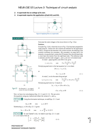
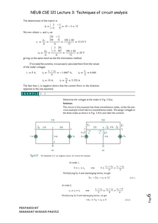
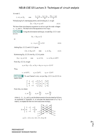
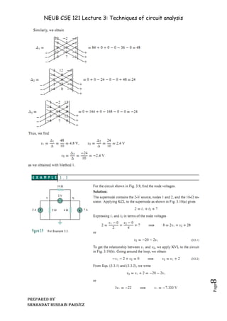
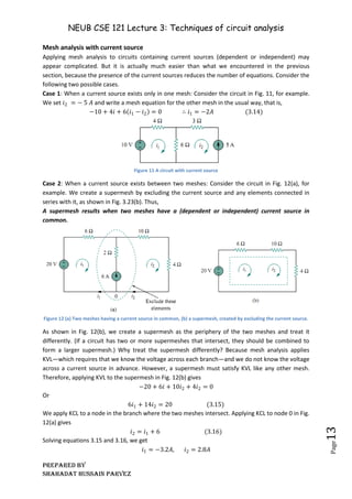
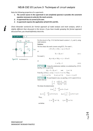
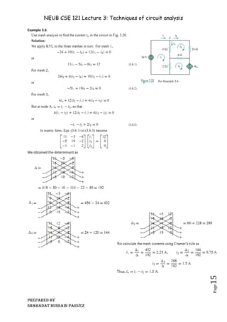
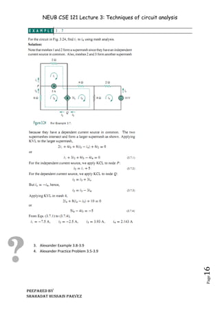
NEUB CSE 121 Lecture 3: Techniques of circuit analysis
Prepared BY
Shahadat Hussain Parvez
Page
1
Although simple circuits can be analyzed using KCL, KVL and Ohm’s Law alone, it becomes
cumbersome for large circuits with many nodes & loops and is not a viable option. As a result, two
other techniques based on these laws are developed that can be used to analyze large circuits. These
two techniques are Nodal analysis and Mesh analysis
Nodal Analysis
Nodal analysis provides a general procedure for analyzing circuits using node voltages as the circuit
variables. Choosing node voltages instead of element voltages as circuit variables is convenient and
reduces the number of equations one must solve simultaneously.
To simplify matters, initially we shall assume that circuits do not contain voltage sources. Circuits
that contain voltage sources will be analyzed later.
In nodal analysis, we are interested in finding the node voltages. Given a circuit with n nodes without
voltage sources, the nodal analysis of the circuit involves taking the following three steps.
1. Select a node as the reference node. Assign voltages v1, v2,...,vn− 1 to the remaining n − 1
nodes. The voltages are referenced with respect to the reference node.
2. Apply KCL to each of the n − 1 non reference nodes. Use Ohm’s law to express the branch
currents in terms of node voltages.
3. Solve the resulting simultaneous equations to obtain the unknown node voltages.
The first step in nodal analysis is selecting a node as the reference or datum node. The reference
node is commonly called the ground since it is assumed to have zero potential. A reference node is
indicated by any of the three symbols in Fig. 1. The type of ground in Fig. 1(b) is called a chassis
ground and is used in devices where the case, enclosure, or chassis acts as a reference point for all
circuits. When the potential of the earth is used as reference, we use the earth ground in Fig. 1(a) or
(c). We shall always use the symbol in Fig. 1(b).
Figure 1 Common symbols for indicating reference node
Once we have selected a reference node, we assign voltage designations to non-reference nodes.
Consider, for example, the circuit in Fig. 2(a). Node 0 is the reference node (v = 0), while nodes 1 and
2 are assigned voltages 𝑣1 and 𝑣2, respectively. Keep in mind that the node voltages are defined
with respect to the reference node. As illustrated in Fig. 2(a), each node voltage is the voltage rise
from the reference node to the corresponding non-reference node or simply the voltage of that
node with respect to the reference node.
Figure 2 Typical circuit for nodal analysis
NEUB CSE 121 Lecture 3: Techniques of circuit analysis
Prepared BY
Shahadat Hussain Parvez
Page
2
As the second step, we apply KCL to each non-reference node in the circuit. To avoid putting too
much information on the same circuit, the circuit in Fig. 2(a) is redrawn in Fig. 2(b), where we now
add 𝑖1, 𝑖2, and 𝑖3 as the currents through resistors R1, R2, and R3, respectively. At node 1, applying
KCL gives
𝐼1 = 𝐼2 + 𝑖1 + 𝑖2
At node 2
𝐼2 + 𝑖2 = 𝑖3
We now apply Ohm’s law to express the unknown currents 𝑖1, 𝑖2, and 𝑖3 in terms of node voltages.
The key idea to bear in mind is that, since resistance is a passive element, by the passive sign
convention, current must always flow from a higher potential to a lower potential.
We can express this principle as
𝑖 =
𝑣ℎ𝑖𝑔ℎ𝑒𝑟 − 𝑣𝑙𝑜𝑤𝑒𝑟
𝑅
For the circuit in Fig. 2(b) we can obtain
𝑖1 =
𝑣1 − 0
𝑅1
𝑖2 =
𝑣1 − 𝑣2
𝑅2
𝑖3 =
𝑣2 − 0
𝑅3
Substituting equations 3.3 in equations 3.1 we get
𝐼1 = 𝐼2 +
𝑣1
𝑅1
+
𝑣1 − 𝑣2
𝑅2
𝑜𝑟, 𝐼1 − 𝐼2 =
𝑣1
𝑅1
+
𝑣1 − 𝑣2
𝑅2
𝑜𝑟, 𝐼1 − 𝐼2 =
𝑣1
𝑅1
+
𝑣1
𝑅2
−
𝑣2
𝑅2
(3.4)
𝐼2 +
𝑣1 − 𝑣2
𝑅2
=
𝑣2
𝑅3
(3.5)
We can write equations 3.4 and 3.5 in matrix form
1
𝑅1
+
1
𝑅2
−
1
𝑅2
−
1
𝑅2
1
𝑅2
+
1
𝑅3
𝑣1
𝑣2
=
𝐼1 − 𝐼2
𝐼2
(3.6)
This matrix can be solved to find the node voltages 𝑣1, 𝑣2.
Nodal analysis (Format approach)
With the observation of equation 3.6 we can develop another approach for generating the equation.
This approach is called format approach. The steps are as follows
1. Choose a reference node and assign a subscripted voltage label to the (N-1) remaining nodes
of the network.
2. The number of equations required for a complete solution is equal to the number of
subscripted voltages (N-1). Column 1 of each equation is formed by summing the
conductance tied to the node of interest and multiplying the result by that subscripted nodal
voltage.
3. We must now consider the mutual terms that, as noted in the preceding example, are always
subtracted from the first column. It is possible to have more than one mutual term if the
nodal voltage of current interest has an element in common with more than one other nodal
(3.1)
(3.2)
(3.3)
NEUB CSE 121 Lecture 3: Techniques of circuit analysis
Prepared BY
Shahadat Hussain Parvez
Page
3
voltage. This will be demonstrated in an example to follow. Each mutual term is the product
of the mutual conductance and the other nodal voltage tied to that conductance.
4. The column to the right of the equality sign is the algebraic sum of the current sources tied to
the node of interest. A current source is assigned a positive sign if it supplies current to a
node and a negative sign if it draws current from the node.
5. Solve the resulting simultaneous equations for the desired voltages.
Consider the example
Figure 3 Figure for nodal analysis (format approach)
Step 1: The figure is redrawn with assigned subscripted voltages in Fig. 4
Figure 4 Defining the nodes for the network of figure 3
Steps 2 to 4
NEUB CSE 121 Lecture 3: Techniques of circuit analysis
Prepared BY
Shahadat Hussain Parvez
Page
4
Nodal analysis with voltage source
We now consider how voltage sources affect nodal analysis. We use the circuit in Fig. 5 for
illustration. Consider the following two possibilities.
Figure 5 A circuit with voltage source and supernode
Case 1: If a voltage source is connected between the reference node and a non-reference node, we
simply set the voltage at the non-reference node equal to the voltage of the voltage source. In Fig. 5,
for example,
𝑣1 = 10 (3.7)
So our analysis is simplified by the knowledge of this node.
Case 1: If the voltage source (dependent or independent) is connected between two non-reference
nodes, the two non-reference nodes form a generalized node or supernode; we apply both KCL and
KVL to determine the node voltages.
A supernode is formed by enclosing a (dependent or independent) voltage source connected
between two non-reference nodes and any elements connected in parallel with it.
In Fig. 5 nodes 2 and 3 form a supernode.
We analyze a circuit with supernodes using the same three steps mentioned in the previously except
that the supernodes are treated differently. Why? Because an essential component of nodal analysis
is applying KCL, which requires knowing the current through each element. There is no way of
knowing the current through a voltage source in advance. However, KCL must be satisfied at a
supernode like any other node. Hence, at the supernode in Fig. 5,
𝑖1 + 𝑖4 = 𝑖2 + 𝑖3 (3.8𝑎)
Or
𝑣1 − 𝑣2
2
+
𝑣1 − 𝑣3
4
=
𝑣2 − 0
8
+
𝑣3 − 0
6
(3.8𝑏)
To apply Kirchhoff’s voltage law to the supernode in Fig. 5, we redraw the circuit as shown in Fig. 6.
Going around the loop in the clockwise direction gives
−𝑣2 + 5 + 𝑣3 = 0 𝑠𝑜, 𝑣2 − 𝑣3 = 0 (3.9)
From Eqs. (3.7), (3.8b), and (3.9), we obtain the node voltages.
Note the following properties of Supernode
1. The voltage source inside the supernode provides a constraint equation needed to solve for
the node voltages.
NEUB CSE 121 Lecture 3: Techniques of circuit analysis
Prepared BY
Shahadat Hussain Parvez
Page
5
2. A supernode has no voltage of its own.
3. A supernode requires the application of both KCL and KVL.
Figure 6 Applying KVL to a supernode
NEUB CSE 121 Lecture 3: Techniques of circuit analysis
Prepared BY
Shahadat Hussain Parvez
Page
6
NEUB CSE 121 Lecture 3: Techniques of circuit analysis
Prepared BY
Shahadat Hussain Parvez
Page
7
NEUB CSE 121 Lecture 3: Techniques of circuit analysis
Prepared BY
Shahadat Hussain Parvez
Page
8
NEUB CSE 121 Lecture 3: Techniques of circuit analysis
Prepared BY
Shahadat Hussain Parvez
Page
9
1. Alexander Example 3.4
2. Alexander Practice Problem 3.1-3.4
NEUB CSE 121 Lecture 3: Techniques of circuit analysis
Prepared BY
Shahadat Hussain Parvez
Page
10
Mesh Analysis
Mesh analysis provides another general procedure for analyzing circuits, using mesh currents as the
circuit variables. Using mesh currents instead of element currents as circuit variables is convenient
and reduces the number of equations that must be solved simultaneously. Recall that a loop is a
closed path with no node passed more than once. A mesh is a loop that does not contain any other
loop within it.
Nodal analysis applies KCL to find unknown voltages in a given circuit, while mesh analysis applies
KVL to find unknown currents. Mesh analysis is not quite as general as nodal analysis because it is
only applicable to a circuit that is planar. A planar circuit is one that can be drawn in a plane with no
branches crossing one another; otherwise it is non-planar. A circuit may have crossing branches and
still be planar if it can be redrawn such that it has no crossing branches. For example, the circuit in
Fig. 7(a) has two crossing branches, but it can be redrawn as in Fig. 7(b). Hence, the circuit in Fig. 7(a)
is planar. However, the circuit in Fig. 8 is non-planar, because there is no way to redraw it and avoid
the branches crossing. Non-planar circuits can be handled using nodal analysis, but they will not be
considered in this course.
Figure 7 (a) A planar circuit with crossing branches, (b) the same circuit redrawn with no crossing branches.
Figure 8 A non-planar circuit
To understand mesh analysis, we should first explain more about what we mean by a mesh.
NEUB CSE 121 Lecture 3: Techniques of circuit analysis
Prepared BY
Shahadat Hussain Parvez
Page
11
A mesh is a loop which does not contain any other loops within it.
In Fig. 9, for example, paths abefa and bcdeb are meshes, but path abcdefa is not a mesh. The
current through a mesh is known as mesh current. In mesh analysis, we are interested in applying
KVL to find the mesh currents in a given circuit.
Figure 9 A circuit with two meshes
In the mesh analysis of a circuit with n meshes, we take the following three steps.
1. Assign mesh currents 𝒊𝟏, 𝒊𝟐, … , 𝒊𝒏 to the n meshes.
2. Apply KVL to each of the n meshes. Use Ohm’s law to express the voltages in terms of the
mesh currents.
3. Solve the resulting n simultaneous equations to get the mesh currents.
To illustrate the steps, consider the circuit in Fig. 9. The first step requires that mesh currents 𝑖1 and
𝑖2 are assigned to meshes 1 and 2. Although a mesh current may be assigned to each mesh in an
arbitrary direction, it is conventional to assume that each mesh current flows clockwise.
As the second step, we apply KVL to each mesh. Applying KVL to mesh 1, we obtain
−𝑉1 + 𝑅1𝑖𝑖 + 𝑅3 𝑖1 − 𝑖2 = 0
Or
𝑅1 + 𝑅3 𝑖1 − 𝑅3𝑖2 = 𝑉1 (3.10)
For mesh 2, applying KVL gives
𝑅2𝑖2 + 𝑉2 + 𝑅3 𝑖2 − 𝑖1 = 0
Or
−𝑅3𝑖1 + 𝑅2 + 𝑅3 𝑖2 = −𝑉2 (3.11)
Note in Eq. (3.10) that the coefficient of 𝑖1 is the sum of the resistances in the first mesh, while the
coefficient of 𝑖2 is the negative of the resistance common to meshes 1 and 2. Now observe that the
same is true in Eq. (3.11). This can serve as a shortcut way of writing the mesh equations. We will
exploit this idea later.
The third step is to solve for the mesh currents. Putting Eqs. (3.10) and (3.11) in matrix form yields
𝑅1 + 𝑅3 −𝑅3
−𝑅3 𝑅2 + 𝑅3
𝑖1
𝑖2
=
𝑉1
𝑉2
(3.12)
which can be solved to obtain the mesh currents 𝑖1 and 𝑖2. Any appropriate method can be used to
solve the simultaneous equations.
Notice that the branch currents are different from the mesh currents unless the mesh is isolated. To
distinguish between the two types of currents, we use 𝑖 for a mesh current and 𝐼 for a branch
current. The current elements 𝐼1, 𝐼2, 𝑎𝑛𝑑 𝐼3 are algebraic sums of the mesh currents. It is evident
from Fig. 9 that
𝐼1 = 𝑖1, 𝐼2 = 𝑖2, 𝐼3 = 𝑖1 − 𝑖2 (3.13)
NEUB CSE 121 Lecture 3: Techniques of circuit analysis
Prepared BY
Shahadat Hussain Parvez
Page
12
Mesh analysis (Format Approach)
Now that the basis for the mesh-analysis approach has been established, we will now examine a
technique for writing the mesh equations more rapidly and usually with fewer errors. As an aid in
introducing the procedure, a circuit is drawn in Fig. 10 with the assigned loop currents. (Note that
each loop current has a clockwise direction.)
The equations obtained are
−7𝐼1 + 6𝐼2 = 5
6𝐼1 − 8𝐼2 = −10
Which can be written as
7𝐼1 − 6𝐼2 = −5
8𝐼2 − 6𝐼1 = 10
And expanded as
Note in the above equations that column 1 is composed of a loop current times the sum of the
resistors through which that loop current passes. Column 2 is the product of the resistors common
to another loop current times that other loop current. Note that in each equation, this column is
subtracted from column 1. Column 3 is the algebraic sum of the voltage sources through which the
loop current of interest passes. A source is assigned a positive sign if the loop current passes from
the negative to the positive terminal, and a negative value is assigned if the polarities are reversed.
The comments above are correct only for a standard direction of loop current in each window, the
one chosen being the clockwise direction.
The above statements can be extended to develop the following format approach to mesh analysis:
1. Assign a loop current to each independent, closed loop (as in the previous section) in a
clockwise direction.
2. The number of required equations is equal to the number of chosen independent, closed
loops. Column 1 of each equation is formed by summing the resistance values of those
resistors through which the loop current of interest passes and multiplying the result by that
loop current.
3. We must now consider the mutual terms, which, as noted in the examples above, are always
subtracted from the first column. A mutual term is simply any resistive element having an
additional loop current passing through it. It is possible to have more than one mutual term if
the loop current of interest has an element in common with more than one other loop
current. This will be demonstrated in an example to follow. Each term is the product of the
mutual resistor and the other loop current passing through the same element.
4. The column to the right of the equality sign is the algebraic sum of the voltage sources
through which the loop current of interest passes. Positive signs are assigned to those
sources of voltage having a polarity such that the loop current passes from the negative to
the positive terminal. A negative sign is assigned to those potentials for which the reverse is
true.
5. Solve the resulting simultaneous equations for the desired loop currents.
Figure 10 Circuit for mesh analysis
NEUB CSE 121 Lecture 3: Techniques of circuit analysis
Prepared BY
Shahadat Hussain Parvez
Page
13
Mesh analysis with current source
Applying mesh analysis to circuits containing current sources (dependent or independent) may
appear complicated. But it is actually much easier than what we encountered in the previous
section, because the presence of the current sources reduces the number of equations. Consider the
following two possible cases.
Case 1: When a current source exists only in one mesh: Consider the circuit in Fig. 11, for example.
We set 𝑖2 = − 5 𝐴 and write a mesh equation for the other mesh in the usual way, that is,
−10 + 4𝑖 + 6 𝑖1 − 𝑖2 = 0 ∴ 𝑖1 = −2𝐴 (3.14)
Figure 11 A circuit with current source
Case 2: When a current source exists between two meshes: Consider the circuit in Fig. 12(a), for
example. We create a supermesh by excluding the current source and any elements connected in
series with it, as shown in Fig. 3.23(b). Thus,
A supermesh results when two meshes have a (dependent or independent) current source in
common.
Figure 12 (a) Two meshes having a current source in common, (b) a supermesh, created by excluding the current source.
As shown in Fig. 12(b), we create a supermesh as the periphery of the two meshes and treat it
differently. (If a circuit has two or more supermeshes that intersect, they should be combined to
form a larger supermesh.) Why treat the supermesh differently? Because mesh analysis applies
KVL—which requires that we know the voltage across each branch—and we do not know the voltage
across a current source in advance. However, a supermesh must satisfy KVL like any other mesh.
Therefore, applying KVL to the supermesh in Fig. 12(b) gives
−20 + 6𝑖 + 10𝑖2 + 4𝑖2 = 0
Or
6𝑖1 + 14𝑖2 = 20 (3.15)
We apply KCL to a node in the branch where the two meshes intersect. Applying KCL to node 0 in Fig.
12(a) gives
𝑖2 = 𝑖1 + 6 (3.16)
Solving equations 3.15 and 3.16, we get
𝑖1 = −3.2𝐴, 𝑖2 = 2.8𝐴
NEUB CSE 121 Lecture 3: Techniques of circuit analysis
Prepared BY
Shahadat Hussain Parvez
Page
14
Note the following properties of a supermesh:
1. The current source in the supermesh is not completely ignored; it provides the constraint
equation necessary to solve for the mesh currents.
2. A supermesh has no current of its own.
3. A supermesh requires the application of both KVL and KCL.
Check Alexander section3.6 for Format approach of nodal analysis and mesh analysis, which is
slightly different than discussed in this lecture. If you have trouble grasping the format approach
discussed here, you should definitely check this.
NEUB CSE 121 Lecture 3: Techniques of circuit analysis
Prepared BY
Shahadat Hussain Parvez
Page
15
Example 3.6
We obtained the determinant as
NEUB CSE 121 Lecture 3: Techniques of circuit analysis
Prepared BY
Shahadat Hussain Parvez
Page
16
3. Alexander Example 3.8-3.9
4. Alexander Practice Problem 3.5-3.9

neub-cse-121-lec-3.pdf Basic-Electric-and-Circuit

  • 1.
    NEUB CSE 121Lecture 3: Techniques of circuit analysis Prepared BY Shahadat Hussain Parvez Page 1 Although simple circuits can be analyzed using KCL, KVL and Ohm’s Law alone, it becomes cumbersome for large circuits with many nodes & loops and is not a viable option. As a result, two other techniques based on these laws are developed that can be used to analyze large circuits. These two techniques are Nodal analysis and Mesh analysis Nodal Analysis Nodal analysis provides a general procedure for analyzing circuits using node voltages as the circuit variables. Choosing node voltages instead of element voltages as circuit variables is convenient and reduces the number of equations one must solve simultaneously. To simplify matters, initially we shall assume that circuits do not contain voltage sources. Circuits that contain voltage sources will be analyzed later. In nodal analysis, we are interested in finding the node voltages. Given a circuit with n nodes without voltage sources, the nodal analysis of the circuit involves taking the following three steps. 1. Select a node as the reference node. Assign voltages v1, v2,...,vn− 1 to the remaining n − 1 nodes. The voltages are referenced with respect to the reference node. 2. Apply KCL to each of the n − 1 non reference nodes. Use Ohm’s law to express the branch currents in terms of node voltages. 3. Solve the resulting simultaneous equations to obtain the unknown node voltages. The first step in nodal analysis is selecting a node as the reference or datum node. The reference node is commonly called the ground since it is assumed to have zero potential. A reference node is indicated by any of the three symbols in Fig. 1. The type of ground in Fig. 1(b) is called a chassis ground and is used in devices where the case, enclosure, or chassis acts as a reference point for all circuits. When the potential of the earth is used as reference, we use the earth ground in Fig. 1(a) or (c). We shall always use the symbol in Fig. 1(b). Figure 1 Common symbols for indicating reference node Once we have selected a reference node, we assign voltage designations to non-reference nodes. Consider, for example, the circuit in Fig. 2(a). Node 0 is the reference node (v = 0), while nodes 1 and 2 are assigned voltages 𝑣1 and 𝑣2, respectively. Keep in mind that the node voltages are defined with respect to the reference node. As illustrated in Fig. 2(a), each node voltage is the voltage rise from the reference node to the corresponding non-reference node or simply the voltage of that node with respect to the reference node. Figure 2 Typical circuit for nodal analysis
  • 2.
    NEUB CSE 121Lecture 3: Techniques of circuit analysis Prepared BY Shahadat Hussain Parvez Page 2 As the second step, we apply KCL to each non-reference node in the circuit. To avoid putting too much information on the same circuit, the circuit in Fig. 2(a) is redrawn in Fig. 2(b), where we now add 𝑖1, 𝑖2, and 𝑖3 as the currents through resistors R1, R2, and R3, respectively. At node 1, applying KCL gives 𝐼1 = 𝐼2 + 𝑖1 + 𝑖2 At node 2 𝐼2 + 𝑖2 = 𝑖3 We now apply Ohm’s law to express the unknown currents 𝑖1, 𝑖2, and 𝑖3 in terms of node voltages. The key idea to bear in mind is that, since resistance is a passive element, by the passive sign convention, current must always flow from a higher potential to a lower potential. We can express this principle as 𝑖 = 𝑣ℎ𝑖𝑔ℎ𝑒𝑟 − 𝑣𝑙𝑜𝑤𝑒𝑟 𝑅 For the circuit in Fig. 2(b) we can obtain 𝑖1 = 𝑣1 − 0 𝑅1 𝑖2 = 𝑣1 − 𝑣2 𝑅2 𝑖3 = 𝑣2 − 0 𝑅3 Substituting equations 3.3 in equations 3.1 we get 𝐼1 = 𝐼2 + 𝑣1 𝑅1 + 𝑣1 − 𝑣2 𝑅2 𝑜𝑟, 𝐼1 − 𝐼2 = 𝑣1 𝑅1 + 𝑣1 − 𝑣2 𝑅2 𝑜𝑟, 𝐼1 − 𝐼2 = 𝑣1 𝑅1 + 𝑣1 𝑅2 − 𝑣2 𝑅2 (3.4) 𝐼2 + 𝑣1 − 𝑣2 𝑅2 = 𝑣2 𝑅3 (3.5) We can write equations 3.4 and 3.5 in matrix form 1 𝑅1 + 1 𝑅2 − 1 𝑅2 − 1 𝑅2 1 𝑅2 + 1 𝑅3 𝑣1 𝑣2 = 𝐼1 − 𝐼2 𝐼2 (3.6) This matrix can be solved to find the node voltages 𝑣1, 𝑣2. Nodal analysis (Format approach) With the observation of equation 3.6 we can develop another approach for generating the equation. This approach is called format approach. The steps are as follows 1. Choose a reference node and assign a subscripted voltage label to the (N-1) remaining nodes of the network. 2. The number of equations required for a complete solution is equal to the number of subscripted voltages (N-1). Column 1 of each equation is formed by summing the conductance tied to the node of interest and multiplying the result by that subscripted nodal voltage. 3. We must now consider the mutual terms that, as noted in the preceding example, are always subtracted from the first column. It is possible to have more than one mutual term if the nodal voltage of current interest has an element in common with more than one other nodal (3.1) (3.2) (3.3)
  • 3.
    NEUB CSE 121Lecture 3: Techniques of circuit analysis Prepared BY Shahadat Hussain Parvez Page 3 voltage. This will be demonstrated in an example to follow. Each mutual term is the product of the mutual conductance and the other nodal voltage tied to that conductance. 4. The column to the right of the equality sign is the algebraic sum of the current sources tied to the node of interest. A current source is assigned a positive sign if it supplies current to a node and a negative sign if it draws current from the node. 5. Solve the resulting simultaneous equations for the desired voltages. Consider the example Figure 3 Figure for nodal analysis (format approach) Step 1: The figure is redrawn with assigned subscripted voltages in Fig. 4 Figure 4 Defining the nodes for the network of figure 3 Steps 2 to 4
  • 4.
    NEUB CSE 121Lecture 3: Techniques of circuit analysis Prepared BY Shahadat Hussain Parvez Page 4 Nodal analysis with voltage source We now consider how voltage sources affect nodal analysis. We use the circuit in Fig. 5 for illustration. Consider the following two possibilities. Figure 5 A circuit with voltage source and supernode Case 1: If a voltage source is connected between the reference node and a non-reference node, we simply set the voltage at the non-reference node equal to the voltage of the voltage source. In Fig. 5, for example, 𝑣1 = 10 (3.7) So our analysis is simplified by the knowledge of this node. Case 1: If the voltage source (dependent or independent) is connected between two non-reference nodes, the two non-reference nodes form a generalized node or supernode; we apply both KCL and KVL to determine the node voltages. A supernode is formed by enclosing a (dependent or independent) voltage source connected between two non-reference nodes and any elements connected in parallel with it. In Fig. 5 nodes 2 and 3 form a supernode. We analyze a circuit with supernodes using the same three steps mentioned in the previously except that the supernodes are treated differently. Why? Because an essential component of nodal analysis is applying KCL, which requires knowing the current through each element. There is no way of knowing the current through a voltage source in advance. However, KCL must be satisfied at a supernode like any other node. Hence, at the supernode in Fig. 5, 𝑖1 + 𝑖4 = 𝑖2 + 𝑖3 (3.8𝑎) Or 𝑣1 − 𝑣2 2 + 𝑣1 − 𝑣3 4 = 𝑣2 − 0 8 + 𝑣3 − 0 6 (3.8𝑏) To apply Kirchhoff’s voltage law to the supernode in Fig. 5, we redraw the circuit as shown in Fig. 6. Going around the loop in the clockwise direction gives −𝑣2 + 5 + 𝑣3 = 0 𝑠𝑜, 𝑣2 − 𝑣3 = 0 (3.9) From Eqs. (3.7), (3.8b), and (3.9), we obtain the node voltages. Note the following properties of Supernode 1. The voltage source inside the supernode provides a constraint equation needed to solve for the node voltages.
  • 5.
    NEUB CSE 121Lecture 3: Techniques of circuit analysis Prepared BY Shahadat Hussain Parvez Page 5 2. A supernode has no voltage of its own. 3. A supernode requires the application of both KCL and KVL. Figure 6 Applying KVL to a supernode
  • 6.
    NEUB CSE 121Lecture 3: Techniques of circuit analysis Prepared BY Shahadat Hussain Parvez Page 6
  • 7.
    NEUB CSE 121Lecture 3: Techniques of circuit analysis Prepared BY Shahadat Hussain Parvez Page 7
  • 8.
    NEUB CSE 121Lecture 3: Techniques of circuit analysis Prepared BY Shahadat Hussain Parvez Page 8
  • 9.
    NEUB CSE 121Lecture 3: Techniques of circuit analysis Prepared BY Shahadat Hussain Parvez Page 9 1. Alexander Example 3.4 2. Alexander Practice Problem 3.1-3.4
  • 10.
    NEUB CSE 121Lecture 3: Techniques of circuit analysis Prepared BY Shahadat Hussain Parvez Page 10 Mesh Analysis Mesh analysis provides another general procedure for analyzing circuits, using mesh currents as the circuit variables. Using mesh currents instead of element currents as circuit variables is convenient and reduces the number of equations that must be solved simultaneously. Recall that a loop is a closed path with no node passed more than once. A mesh is a loop that does not contain any other loop within it. Nodal analysis applies KCL to find unknown voltages in a given circuit, while mesh analysis applies KVL to find unknown currents. Mesh analysis is not quite as general as nodal analysis because it is only applicable to a circuit that is planar. A planar circuit is one that can be drawn in a plane with no branches crossing one another; otherwise it is non-planar. A circuit may have crossing branches and still be planar if it can be redrawn such that it has no crossing branches. For example, the circuit in Fig. 7(a) has two crossing branches, but it can be redrawn as in Fig. 7(b). Hence, the circuit in Fig. 7(a) is planar. However, the circuit in Fig. 8 is non-planar, because there is no way to redraw it and avoid the branches crossing. Non-planar circuits can be handled using nodal analysis, but they will not be considered in this course. Figure 7 (a) A planar circuit with crossing branches, (b) the same circuit redrawn with no crossing branches. Figure 8 A non-planar circuit To understand mesh analysis, we should first explain more about what we mean by a mesh.
  • 11.
    NEUB CSE 121Lecture 3: Techniques of circuit analysis Prepared BY Shahadat Hussain Parvez Page 11 A mesh is a loop which does not contain any other loops within it. In Fig. 9, for example, paths abefa and bcdeb are meshes, but path abcdefa is not a mesh. The current through a mesh is known as mesh current. In mesh analysis, we are interested in applying KVL to find the mesh currents in a given circuit. Figure 9 A circuit with two meshes In the mesh analysis of a circuit with n meshes, we take the following three steps. 1. Assign mesh currents 𝒊𝟏, 𝒊𝟐, … , 𝒊𝒏 to the n meshes. 2. Apply KVL to each of the n meshes. Use Ohm’s law to express the voltages in terms of the mesh currents. 3. Solve the resulting n simultaneous equations to get the mesh currents. To illustrate the steps, consider the circuit in Fig. 9. The first step requires that mesh currents 𝑖1 and 𝑖2 are assigned to meshes 1 and 2. Although a mesh current may be assigned to each mesh in an arbitrary direction, it is conventional to assume that each mesh current flows clockwise. As the second step, we apply KVL to each mesh. Applying KVL to mesh 1, we obtain −𝑉1 + 𝑅1𝑖𝑖 + 𝑅3 𝑖1 − 𝑖2 = 0 Or 𝑅1 + 𝑅3 𝑖1 − 𝑅3𝑖2 = 𝑉1 (3.10) For mesh 2, applying KVL gives 𝑅2𝑖2 + 𝑉2 + 𝑅3 𝑖2 − 𝑖1 = 0 Or −𝑅3𝑖1 + 𝑅2 + 𝑅3 𝑖2 = −𝑉2 (3.11) Note in Eq. (3.10) that the coefficient of 𝑖1 is the sum of the resistances in the first mesh, while the coefficient of 𝑖2 is the negative of the resistance common to meshes 1 and 2. Now observe that the same is true in Eq. (3.11). This can serve as a shortcut way of writing the mesh equations. We will exploit this idea later. The third step is to solve for the mesh currents. Putting Eqs. (3.10) and (3.11) in matrix form yields 𝑅1 + 𝑅3 −𝑅3 −𝑅3 𝑅2 + 𝑅3 𝑖1 𝑖2 = 𝑉1 𝑉2 (3.12) which can be solved to obtain the mesh currents 𝑖1 and 𝑖2. Any appropriate method can be used to solve the simultaneous equations. Notice that the branch currents are different from the mesh currents unless the mesh is isolated. To distinguish between the two types of currents, we use 𝑖 for a mesh current and 𝐼 for a branch current. The current elements 𝐼1, 𝐼2, 𝑎𝑛𝑑 𝐼3 are algebraic sums of the mesh currents. It is evident from Fig. 9 that 𝐼1 = 𝑖1, 𝐼2 = 𝑖2, 𝐼3 = 𝑖1 − 𝑖2 (3.13)
  • 12.
    NEUB CSE 121Lecture 3: Techniques of circuit analysis Prepared BY Shahadat Hussain Parvez Page 12 Mesh analysis (Format Approach) Now that the basis for the mesh-analysis approach has been established, we will now examine a technique for writing the mesh equations more rapidly and usually with fewer errors. As an aid in introducing the procedure, a circuit is drawn in Fig. 10 with the assigned loop currents. (Note that each loop current has a clockwise direction.) The equations obtained are −7𝐼1 + 6𝐼2 = 5 6𝐼1 − 8𝐼2 = −10 Which can be written as 7𝐼1 − 6𝐼2 = −5 8𝐼2 − 6𝐼1 = 10 And expanded as Note in the above equations that column 1 is composed of a loop current times the sum of the resistors through which that loop current passes. Column 2 is the product of the resistors common to another loop current times that other loop current. Note that in each equation, this column is subtracted from column 1. Column 3 is the algebraic sum of the voltage sources through which the loop current of interest passes. A source is assigned a positive sign if the loop current passes from the negative to the positive terminal, and a negative value is assigned if the polarities are reversed. The comments above are correct only for a standard direction of loop current in each window, the one chosen being the clockwise direction. The above statements can be extended to develop the following format approach to mesh analysis: 1. Assign a loop current to each independent, closed loop (as in the previous section) in a clockwise direction. 2. The number of required equations is equal to the number of chosen independent, closed loops. Column 1 of each equation is formed by summing the resistance values of those resistors through which the loop current of interest passes and multiplying the result by that loop current. 3. We must now consider the mutual terms, which, as noted in the examples above, are always subtracted from the first column. A mutual term is simply any resistive element having an additional loop current passing through it. It is possible to have more than one mutual term if the loop current of interest has an element in common with more than one other loop current. This will be demonstrated in an example to follow. Each term is the product of the mutual resistor and the other loop current passing through the same element. 4. The column to the right of the equality sign is the algebraic sum of the voltage sources through which the loop current of interest passes. Positive signs are assigned to those sources of voltage having a polarity such that the loop current passes from the negative to the positive terminal. A negative sign is assigned to those potentials for which the reverse is true. 5. Solve the resulting simultaneous equations for the desired loop currents. Figure 10 Circuit for mesh analysis
  • 13.
    NEUB CSE 121Lecture 3: Techniques of circuit analysis Prepared BY Shahadat Hussain Parvez Page 13 Mesh analysis with current source Applying mesh analysis to circuits containing current sources (dependent or independent) may appear complicated. But it is actually much easier than what we encountered in the previous section, because the presence of the current sources reduces the number of equations. Consider the following two possible cases. Case 1: When a current source exists only in one mesh: Consider the circuit in Fig. 11, for example. We set 𝑖2 = − 5 𝐴 and write a mesh equation for the other mesh in the usual way, that is, −10 + 4𝑖 + 6 𝑖1 − 𝑖2 = 0 ∴ 𝑖1 = −2𝐴 (3.14) Figure 11 A circuit with current source Case 2: When a current source exists between two meshes: Consider the circuit in Fig. 12(a), for example. We create a supermesh by excluding the current source and any elements connected in series with it, as shown in Fig. 3.23(b). Thus, A supermesh results when two meshes have a (dependent or independent) current source in common. Figure 12 (a) Two meshes having a current source in common, (b) a supermesh, created by excluding the current source. As shown in Fig. 12(b), we create a supermesh as the periphery of the two meshes and treat it differently. (If a circuit has two or more supermeshes that intersect, they should be combined to form a larger supermesh.) Why treat the supermesh differently? Because mesh analysis applies KVL—which requires that we know the voltage across each branch—and we do not know the voltage across a current source in advance. However, a supermesh must satisfy KVL like any other mesh. Therefore, applying KVL to the supermesh in Fig. 12(b) gives −20 + 6𝑖 + 10𝑖2 + 4𝑖2 = 0 Or 6𝑖1 + 14𝑖2 = 20 (3.15) We apply KCL to a node in the branch where the two meshes intersect. Applying KCL to node 0 in Fig. 12(a) gives 𝑖2 = 𝑖1 + 6 (3.16) Solving equations 3.15 and 3.16, we get 𝑖1 = −3.2𝐴, 𝑖2 = 2.8𝐴
  • 14.
    NEUB CSE 121Lecture 3: Techniques of circuit analysis Prepared BY Shahadat Hussain Parvez Page 14 Note the following properties of a supermesh: 1. The current source in the supermesh is not completely ignored; it provides the constraint equation necessary to solve for the mesh currents. 2. A supermesh has no current of its own. 3. A supermesh requires the application of both KVL and KCL. Check Alexander section3.6 for Format approach of nodal analysis and mesh analysis, which is slightly different than discussed in this lecture. If you have trouble grasping the format approach discussed here, you should definitely check this.
  • 15.
    NEUB CSE 121Lecture 3: Techniques of circuit analysis Prepared BY Shahadat Hussain Parvez Page 15 Example 3.6 We obtained the determinant as
  • 16.
    NEUB CSE 121Lecture 3: Techniques of circuit analysis Prepared BY Shahadat Hussain Parvez Page 16 3. Alexander Example 3.8-3.9 4. Alexander Practice Problem 3.5-3.9