Download to read offline
![INTERNATIONAL RESEARCH JOURNAL OF ENGINEERING AND TECHNOLOGY (IRJET) E-ISSN: 2395-0056
VOLUME: 06 ISSUE: 05 | MAY 2019 WWW.IRJET.NET P-ISSN: 2395-0072
© 2019, IRJET | Impact Factor value: 7.211 | ISO 9001:2008 Certified Journal | Page 2316
Design and Testing of 10W SSPA based S band Transmitting
Module
Divya B N1, Mrs. Shakunthala C2
1M. Tech CAID, Dept. of Electrical & Electronics Engineering, The National Institute of Engineering, Mysuru,
Karnataka, India
2Assistant Professor, Dept. of Electrical & Electronics Engineering, The National Institute of Engineering, Mysuru,
Karnataka, India.
--------------------------------------------------------***--------------------------------------------------------
ABSTRACT:-Future of weather radar lies in Phase Array
Technology with its advanced multifunction capability and
performance. Solid State Power Amplifier (SSPA) using GaN
apparently presents many benefits including reliability over
Travelling Wave Tube Amplifier (TWTA). The SSPA forms an
integral unit of a phased array antenna used in
Multifunction Phase Array Radar (MPAR). This paper
describes the design and testing of SSPA based transmitting
module consisting of pre-driver, driver and power amplifier
stage to deliver 10W output power at 2.85GHz(S band
frequency range) .Simulation is carried out using Agilent
ADS software for impedance matching. S parameters
measurements are carried out in the laboratory with
fabricated components using Vector Network Analyzer.
Key words:-Solid State Power Amplifier, S band, S
parameter, impedance matching
I. INTRODUCTION
Radar technology is one of the most advanced methods
used to measure the position of an object at point where
radar is Located, and the distance between the objects. A
radar system usually consists of a transmitter that
generates electromagnetic signals emitted by an antenna in
space. An active electronically scanned and computer
controlled phased array antenna is used by radar, in
antenna theory. Without moving the antenna, the radio
waves can be sent in different direction by means of
electromagnetic control. Each antenna element is
connected to a small solid state transceiver module under
the control of computer that performs the function of
transmitter of antenna.
Multifunction Phase Array Radar (MPAR) is an active
phased array radar having the main features such as
Electronic steering , rapid scanning and capable to
simultaneously perform weather surveillance ,aircraft
surveillance with a single phase array radar operating at
the frequency range of S band. The transmitter module
consisting power amplifier is designed for S-band MPAR
system which is used to provide sufficient energy for radar
signals before transmitting and generating from the
antenna for the implementation of long way
communication and to achieve lower attenuation [2].The
Gallium Nitride (GaN) HEMT is a strategic component for
high performance, wideband transceiver modules and high
performance semiconductor transmitters [3]. High power
density is the important feature of GaN and high voltage
feature decreases the need of voltage conversion, leading to
higher efficiency operation [1].
The radar transmitter generates the high power short
duration RF signals that are radiated into space by the
antenna and having significant characteristics such as
suitable RF bandwidth, high stability to signal processing,
easily modulated to required waveform design, high
efficient and reliable .
Radar transmitter is classified into two types:
High–Power Oscillator transmitter
High–Power-Amplifier transmitter
Power Amplifier Transmitter (PAT) is an active
antenna where each antenna element or group is
designed with an own amplifier such as Magnetron,
Klystron or Solid State Amplifier. Radar with PATs is
fully coherent.
Solid State Power Amplifier (SSPA) is significantly
beneficial over the Travelling Wave Tube Amplifier
(TWTA) with parameters such as size, weight, power,
linearity, efficiency, reliability, output distribution
losses and RF output power.
This paper describes the design and testing of 10W
SSPA based S band transmitting module. The block
diagram of the transceiver module is as shown in the
figure 1. It consists of transmitting and receiver chain.
Transmitting chain consists of 3 stages namely:](https://image.slidesharecdn.com/irjet-v6i5443-190912101744/75/IRJET-Design-and-Testing-of-10W-SSPA-based-S-Band-Transmitting-Module-1-2048.jpg)
![INTERNATIONAL RESEARCH JOURNAL OF ENGINEERING AND TECHNOLOGY (IRJET) E-ISSN: 2395-0056
VOLUME: 06 ISSUE: 05 | MAY 2019 WWW.IRJET.NET P-ISSN: 2395-0072
© 2019, IRJET | Impact Factor value: 7.211 | ISO 9001:2008 Certified Journal | Page 2318
A.STABILITY ANALYSIS
Transistor is operated in the active region by DC biasing
so that the power amplifier performance is improved.
Instability of the device can damage or destroy transistor.
Stabilization circuit is designed to avoid the power
amplifier entering the oscillations causing the decrease of
the gain at lower frequency side. In order to overcome the
stability issue stabilization circuit is designed where
parallel RC circuit is connected to gate side of the CREE
transistor. Stability test is carried out and simulation
results for the stability are shown in figure 2-3.
Figure.2. Stability factor before adding the RC circuit
at 1.9 GHz
Figure.3. Stability factor after adding the RC circuit
at 2.1GHz
B. MATCHING NETWORKS
For impedance transformation, matching networks are
designed usually between the transistor and the
terminations on the input and output side of the amplifier.
In this paper load pull technique is carried out using the
ads software providing the platform to analyze and to find
out the optimum values of source and load impedance
required for design of matching circuits [1]. Impedance
matching technique ensures the maximum power transfer.
Optimum impedance is obtained by load pull test used
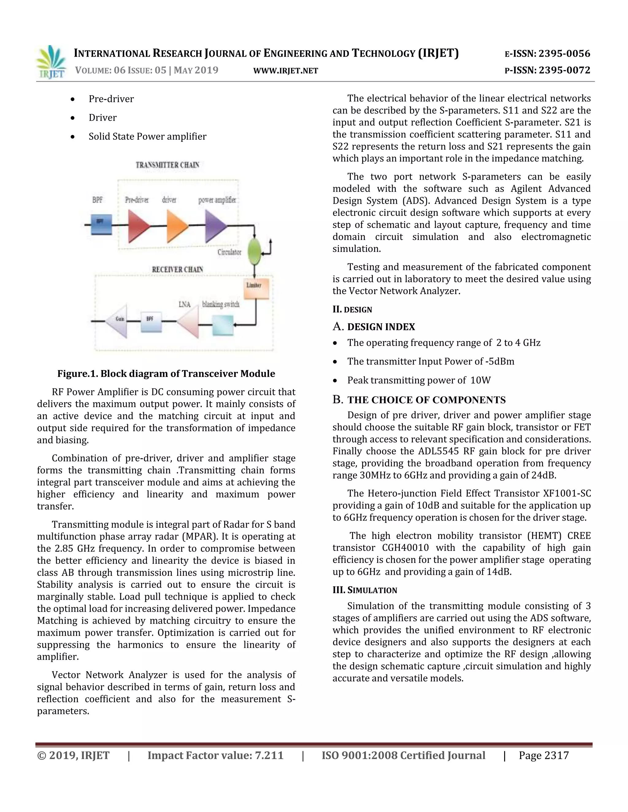
for the Matching Network design. In pre driver design
ADL5545 is used .It is found optimum source and load
impedance are 24.321+j2.073 and 34.889-6.919. The
matching circuit output result with the gain of 21dB and
other s parameter at 2.85 GHz is as shown in figure 4.
In driver design XF1001-SC transistor is used. It is
found optimum source and load impedance are
71.746+j30.531 and 10.793-j7.527. The matching circuit
output result with the gain of 9.957dB and other S
parameter at 2.85 GHz is as shown in figure 5.
In power amplifier design CGH40010F CREE transistor
is used. It is found optimum source and load impedance are
2.95+j*2.29 and 10.79+j*2.29. The matching circuit output
result with the gain of 15.259dB and other S parameter at
2.85 GHz is as shown in figure 6.
Figure.4. Matching circuit output with the gain of
21.194dB at 2.85GHz
1.0 1.5 2.0 2.5 3.0 3.5 4.0 4.5 5.0 5.50.5 6.0
1
2
3
4
5
6
7
8
9
0
10
freq, GHz
K
m4
mu_load
m5
mu_source
m3
m4
freq=
K=1.743
2.100GHz
m5
freq=
mu_load=2.280
900.0MHz
m3
freq=
mu_source=1.152
600.0MHz](https://image.slidesharecdn.com/irjet-v6i5443-190912101744/75/IRJET-Design-and-Testing-of-10W-SSPA-based-S-Band-Transmitting-Module-3-2048.jpg)
![INTERNATIONAL RESEARCH JOURNAL OF ENGINEERING AND TECHNOLOGY (IRJET) E-ISSN: 2395-0056
VOLUME: 06 ISSUE: 05 | MAY 2019 WWW.IRJET.NET P-ISSN: 2395-0072
© 2019, IRJET | Impact Factor value: 7.211 | ISO 9001:2008 Certified Journal | Page 2320
The test result of the fabricated XF1001-SC, driver is as
shown in the figure 10. Gain (S21), S11, S22 parameters of
9.4dB, -8.89dB and -5.1dB are obtained respectively at the
frequency of 2.85GHz.
Figure.10. Network Analyzer of XF1001
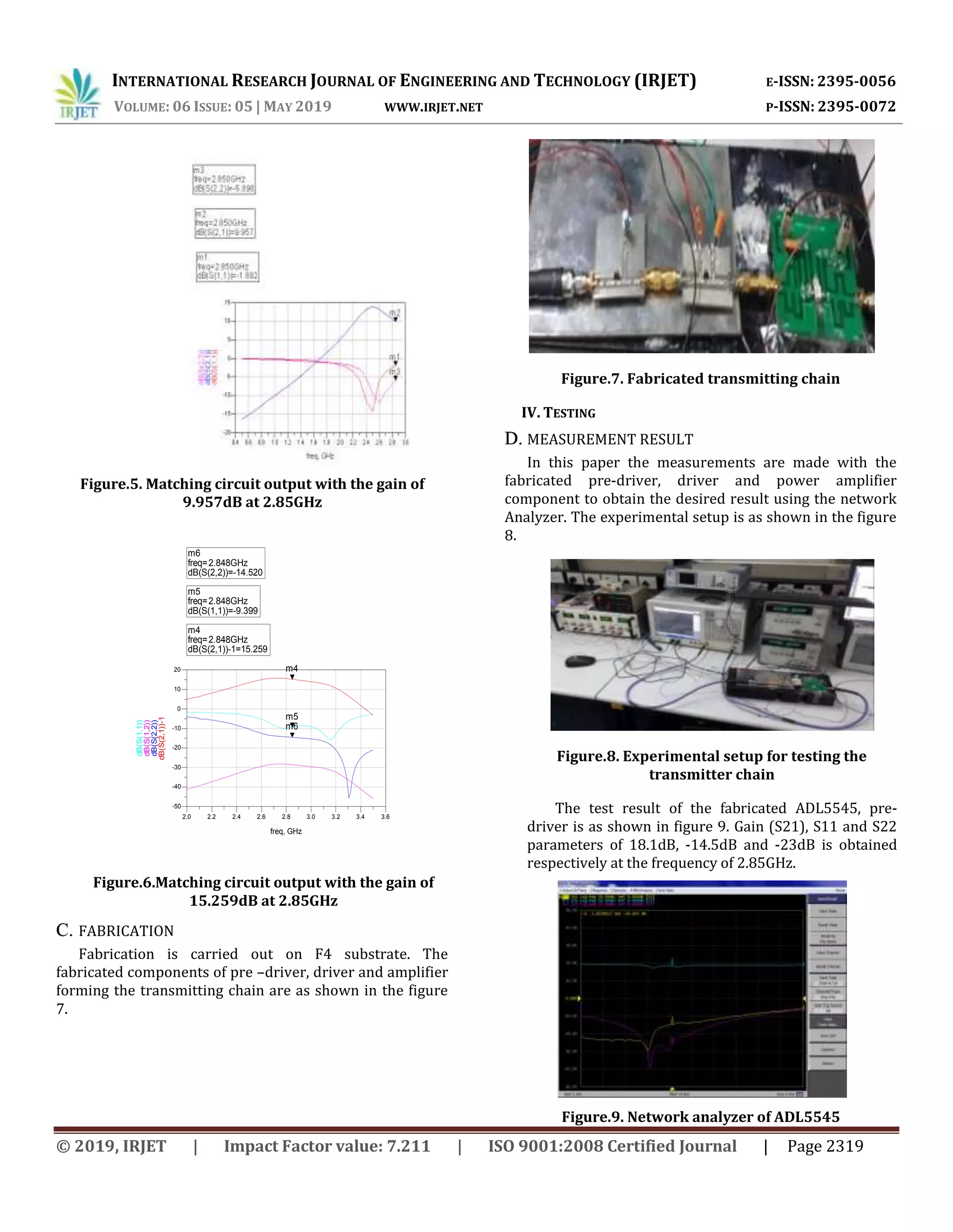
The test result of fabricated CGH40010, power amplifier
is as shown in figure 11.Gain (S21), S11, S22 parameters of
13.2 dB, -5.7 dB and -11.0dB is obtained respectively at
frequency of 2.85GHz.
Figure.11. Network Analyzer of CGH40010
The test result of transmitter chain is as shown in the figure
12. Gain (S21), S11, and S22 parameters of 41.2 dB, -20dB, -
9dB are obtained respectively at frequency of 2.85 GHz.
Figure.12. Network Analyzer of
ADL5545+XF1001+CGH40010
V. CONCLUSION
In this paper design, simulation and testing of 10W
SSPA based S band transmitting module is carried out.
Simulation and testing results were found to be
satisfactory. The test result of transmitter chain shows the
gain of 41.2 dB at the frequency of 2.85GHz. Better gain,
efficiency, linearity and reliability of transmitting module
are achieved.
REFRENCES
[1] Muhammed Hakan Yilmaz, “Design of a wideband 10W
GaN power amplifier,” Thesis for the degree of Master
of Science, Norwegian University of Science and
Technology, Trondheim, July 2011.
[2] Doan Van Truong, Linh Mai, Van-Su Tran, “ 0.5 W S-
band Two-stage Power Amplifier: Research, Design
and Implementation,”2nd International conference on
Recent Advances in Signal Processing,
Telecommunications & computing, IEEE Trans. May.
2018
[3] Gan Shujian, Pei Chen, Chu Ran, “Design of a High-
Efficiency Doherty GaN Power Amplifier,”IEEE
Trans.March 2016
[4] Lianmei Wang, Dong Chen, “Design of Broadband
Power Amplifier based on ADS,”IEEE Trans.
March.2016
[5] Congjie Wu, Yalin Guan, “Design and Simulation of
Driver Stage Power Amplifier,” IEEE workshop on
advanced Research and technology in industrial
applications, IEEE Trans. 2014.
[6] R. Gilmore and L.Besser, “Practical RF Circuit Design
for Modern WirelessSystems,” Volume II Active
Circuits andSystems, Artech House, 2002](https://image.slidesharecdn.com/irjet-v6i5443-190912101744/75/IRJET-Design-and-Testing-of-10W-SSPA-based-S-Band-Transmitting-Module-5-2048.jpg)

This document describes the design and testing of a 10W SSPA-based S-band transmitting module for use in a multifunction phased array radar system. The module consists of three amplification stages - a pre-driver, driver, and power amplifier. Each stage was simulated in Agilent ADS software to optimize impedance matching and ensure stability. A CREE GaN HEMT was selected as the power amplifier due to its high gain and efficiency capabilities. The fabricated module was tested using a vector network analyzer to validate the S-parameter measurements meet specifications.
![[IJET-V1I2P6] Authors :Sarat K Kotamraju, K.Ch.Sri Kavya, A.Gnandeep Reddy, G...](https://cdn.slidesharecdn.com/ss_thumbnails/ijet-v1i2p6-150501052009-conversion-gate02-thumbnail.jpg?width=640&height=640&fit=bounds)