SlideShare a Scribd company logo
1 of 51
Lithography using self assembly: block co-
polymer self assembly, porous anodized
aluminum oxide and nano-sphere lithography
1. Di-block copolymer self assembly overview.
2. Guided (directed, aligned) self assembly.
3. Block copolymer lithography.
4. Anodized aluminum oxide (AAO) overview.
5. Nanofabricating using AAO template
Those are the three most important self-assembly techniques, widely used for nanofabrication, with
numerous publications each year.
Basically, for those who don’t have access or don’t like too much EBL, FIB or imprint, they can often use
self-assembly fabrication to demonstrate their idea.
The most significant advantage of self-assembly is low cost.
The biggest limit: only periodic pattern can be created, usually without long range ordering.
1
ECE 730: Fabrication in the nanoscale: principles, technology and applications
Instructor: Bo Cui, ECE, University of Waterloo; http://ece.uwaterloo.ca/~bcui/
Textbook: Nanofabrication: principles, capabilities and limits, by Zheng Cui
a) A blend of two incompatible homo-polymer
separates into distinct phases on a large scale
(left), whereas block copolymers micro-phase
separate into periodic domains (right).
b) Basic morphologies obtained by different block
copolymer compositions.
Phase separation of block copolymers
1. A mixture of PMMA (Mw=93.9 kg/mol) and
polystyrene (PS, Mw=194.9 kg/mol)
(PS/PMMA=70/30, w/w) was dissolved in
tetrahydrofuran (THF) to form a 5 wt% solution.
2. Polymer film was made by spin-cast the solution
on glass slide.
3. Exposure to cyclohexane at 70oC to dissolve PS.
Phase separation of a blend of
PMMA and PS homo-polymer
Ma, “Fabrication of super-hydrophobic film from PMMA with intrinsic
water contact angle below 90o”, Polymer, 48, 7455-7460 (2007).
PMMA, PS was dissolved
2
“Nanochemistry: a chemical approach to nanomaterials” by Ozin
Typical self assembly behavior for linear block copolymers
3
Typical self assembly behavior for linear block copolymers
4
Block copolymer self-assembly study is started in the bulk phase, as shown above; whereas
thin film is desired for nanofabrication and device application.
When film thickness is well controlled, hole/pillar array or line array pattern can be created.
TEM images of PS-PB diblock copolymer film masks (a,c) and
lithographically patterned silicon nitride (b,d).
One example: self-assembly of PS-PB di-block copolymer
C. Harrison, Science
The most attractive feature of
block copolymer self assembly is
the extremely high resolution,
easily get features down to 10nm.
PS: polystyrene
PB: polybutadiene
5
Line array
Pillar array
Block copolymer thin films
• Film applied by drop casting, dip coating, and spin coating.
• Film is then treated to increase the degree of ordering.
• Such as annealing above the order-disorder transition temperature for several days.
• Or annealing at the presence of solvent vapor (toluene...) to swell the film and make
the polymer more mobile.
• One way to achieve alignment is through
directional solidification strategy
• Such as using a temperature gradient – the film is
heated to above order-disorder transition and
cooled in the presence of such gradient; so that
the ordered phase nucleates at the cool end that
serves as a template and orient the rest of the film.
• Annealing film in the presence of a gradient in
solvent vapor has similar effect.
Film ordered by controlled solvent evaporation.
Advanced Material, 16, 226 (2004)
6
Synthesis: anionic living polymerization
7
B
A
B
A B A
Block copolymer thin films: effect of substrate wetting
Block A is shorter than B
Arranged to minimize surface (interface) energy
8
(left) will result in line array (grating) pattern
(right) will result in hole/pillar array pattern
A forms cylinders
embedded in B
Lithography using self assembly: block co-
polymer self assembly, porous anodized
aluminum oxide and nano-sphere lithography
1. Di-block copolymer self assembly overview.
2. Guided (directed, aligned) self assembly.
3. Block copolymer lithography.
4. Anodized aluminum oxide (AAO) overview.
5. Nanofabricating using AAO template
9
Micro-phase separated block copolymer can be directed/aligned by:
• Electric field
• Shearing force
• Surface control of wettability
• Chemical pattern on surface
• Nano-structured surface
• Spatial confinement by surface relief pattern in substrate and mold
• Void in a range of porous host
Guided block copolymer self assembly
for long range ordering and periodicity
10
Alignment by pre-patterning the substrate
Spherical domains assembled from
PS–PFS (polystyrene-
polyferrocenyldimethylsilane) block
copolymer inside patterned SiO2
grooves.
The 1.5 wt.% PS-PFS block copolymer in
toluene solution was spin-coated onto the
grooved substrate and then annealed at
140oC for 48h to obtain a monolayer of
spherical PFS domains in a PS matrix
within the substrate grooves.
Ross, “Templated self-assembly of block copolymers: effect of substrate topography”, Adv. Mater. 15, 1599–1602 (2003).
11
Alignment by shear force
(here for silicon nano-wire fabrication)
Co-polymer on substrate
Press
Pull
One way to create shear force.
Here the etch contrast is increased by staining the block
copolymer by 2 min exposure to the vapor from 0.5%
aqueous RuO4, which selectively reacts with the PS block
and increases its etch resistance, thus permitting Si
nanowires of greater aspect ratio to be fabricated.
a) Fabrication process for a Si nano-wire grid
polarizer using block copolymer lithography.
b) SEM image of the finished Si nano-wire grid on
fused silica.
12
Alignment by shear force (for silicon nano-wire fabrication)
Pitch=30nm
Tapping mode AFM phase images of PS–PHMA thin
films on top of an -Si layer on a fused silica substrate:
a) Quiescently annealed
b) Shear aligned.
Glassy (hard) PS cylinders are shown as light in a dark
rubbery (soft) PHMA matrix.
Polystyrene-b-poly(n-hexyl methacrylate) (PS–
PHMA) diblock copolymer with a molar mass of
21 and 64 kg/mol for the respective blocks.
Chaikin, “Silicon nanowire grid polarizer for very deep ultraviolet fabricated from a
shear-aligned diblock copolymer template”, Optics letters, 32(21), 3125-3127 (2007).
13
Templated self-assembly of block copolymers
Polystyrene “brushes” by EUV-IL (interference
lithography) and surface initiated nitroxide
mediated living free radical polymerization
The PS brush pitch should match that of PS-PMMA self assembly pitch. 14
Polymerization of block-copolymers on
chemically pre-patterned substrates
P. F. Nealey, H. H. Solak et al. Nature 424 (2003)
Polystyrene-block-methyl meth
acrylate (PS-b-PMMA), L0 = 48nm
Thermodynamics dominates
interface widths and domain sizes.
When Ls=47.5nmLo=48nm, block
copolymer is almost defect free.
15
Here chemically patterned
grating with polystyrene “brush”
Block copolymer materials that naturally form simple periodic
structures were directed to assemble into non-regular device oriented
patterns (here an elbow) on chemically nano-patterned substrates.
Mark P. Stoykovich, Marcus Müller,Sang Ouk Kim, Harun H. Solak, Paul F. Nealey, Science, 308, 1442-1446 (2005).
Directed assembly of block copolymer blends
into non-regular device oriented structure
16
Directed assembly of nanoparticle filled block copolymer
17
Alignment by electric field
“Local control of microdomain orientation in diblock copolymer thin films with electric fields”, Science, 273, 931 (1996)
18
Lithography using self assembly: block co-
polymer self assembly, porous anodized
aluminum oxide and nano-sphere lithography
1. Di-block copolymer self assembly overview.
2. Guided (directed, aligned) self assembly.
3. Block copolymer lithography.
4. Anodized aluminum oxide (AAO) overview.
5. Nanofabricating using AAO template
19
Block copolymer lithography (add pattern transfer)
PS: polystyrene
PB: polybutadiene
• Ozone breaks down PB’s C=C double bond.
• OsO4 vapor reacts with PB’s double bond.
Degrade with ozone
Stain with OsO4
20
Os is a hard
RIE mask
Synthesis of nanowires by wetting
a) Gold (or Ag) metal vapor-
deposited onto a preformed PS-
b-PMMA template.
b) After annealing at 180°C for 1
min., gold nanoparticles
segregate selectively to the PS
domains and form chains.
c) Repeated deposition and short-
time annealing increases the
metal loading, forming
continuous conductive
nanowires.
Wettability masks:
Au and Ag go to (“wet”) PS phase
In, Pb, Sn go to PMMA phase
Nature, 414, 735 (2001).
21
Block copolymer lithography using PMMA-PS
1. After deep UV-exposure, polymer chain of PMMA is cut (PMMA
is a positive deep UV lithography resist), making it more soluble
in solvent.
2. Whereas the polystyrene (PS) chain is cross-linked, making it
hard to dissolve by solvent.
3. Therefore, PMMA can be selectively removed by solvents like
acetic acid afterwards.
(PMMA chain can also be broken by UV light at =365nm, but need very long
time exposure, 1 h at 40mW/cm2 intensity)
22
Nanofabrication of vertical nanowires by electroplating
• Aligned by electric field during annealing.
• PS 71%, to obtain 14nm PMMA cylinder.
• Deep UV simultaneously degrades PMMA and cross-link PS.
• Acetic acid dissolve PMMA but not cross-linked PS (polystyrene).
• Methanol is added to aqueous plating solution to better wet hydrophobic PS membrane.
Science, 290, 2126 (2000)
Electric field is for vertical
alignment of self-assembly
23
Density multiplication (here by 9) lithography
A. Top-down and side-view schematics showing the arrangement of PS-b-PDMS block copolymer
molecules in the region surrounding a single post made from cross-linked HSQ resist (by e-beam
lithography). The post and substrate surfaces have been chemically functionalized by a monolayer
of short-chain PDMS brush.
B. A poorly ordered monolayer of BCP (block co-polymer) spherical domains formed on a flat surface (
without template guidance). The boundaries between different grain orientations are indicated
with dashed lines. The inset is a 2D Fourier transform of the domain positions that shows the
absence of long-range order.
C-D. SEM images of ordered BCP spheres formed within a sparse 2D lattice of HSQ
Ross, “Graphoepitaxy of self-assembled block copolymers on two-dimensional periodic patterned templates”, Science, 321, 939-943 (2008).
For the moment, this is considered as the most promising route for bit-patterned magnetic recording
media fabrication (make the mold for nanoimprint lithography), up to 10Tbits/in2 for pitch 8nm.
24
Lithography using self assembly: block co-
polymer self assembly, porous anodized
aluminum oxide and nano-sphere lithography
1. Di-block copolymer self assembly overview.
2. Guided (directed, aligned) self assembly.
3. Block copolymer lithography.
4. Anodized aluminum oxide (AAO) overview.
5. Nanofabricating using AAO template
25
2Al + 3H2O → Al2O3 + 3H2 [G = -8.65  105J]
Aluminum anodization setup
Electrolyte:
Oxalic acid, phosphoric acid,
sulfuric acid …
Anodization:
• A direct current is passed through an
electrolytic solution where the Al sheet is
used as the anode.
• Two processes: dissolving and oxidation
• Naturally formed triangular pore arrays
26
Porous anodized aluminum
Al2O3
Porous Al2O3 membranes
Top surface of the AAO
Bottom surface of the AAO showing
the barrier layer
Cross section of the AAO AAO filter from Whatman Inc.
27
Nano-pore formation mechanism
• Two types of electrical current due to 1) oxide growth, 2) its dissolution.
• The barrier has to be thin to be “transparent” for anions OH- and O2-.
• These ions interacts with Al3+ ions, which can also move under electric field.
• The wall is “pushed” upward by the continuous anodization at the oxide/Al interface.
• Other mechanisms have also been reported.
28
Schematic diagram of the pore formation
at the beginning of the anodization.
1. Formation of barrier oxide on the
entire area.
2. Local field distributions caused by
surface fluctuations.
3. Creation of pores by field-enhanced
or/and temperature-enhanced
dissolution. Some pores stop growing
due to competition among pores.
4. Stable pore growth.
Nano-pore formation mechanism
29
Pore dimensions
Controlling parameters: voltage, electrolyte, temperature and time.
Cell size D  2.5V (nm), V is voltage with a unit volt.
Pore size d  V (nm), depends on pH; but pore can be enlarged in acids.
30
Common acids for AAO
Sulfuric acid generally gives smallest pore diameter and largest pore density.
Standard deviation of pore diameter usually is within 10%.
Oxalic acid
31
Al2O3
Al
AAO membrane production
Wet-etch Al Etch barrier
Commercial membrane: thickness 60m, pore size down to 20nm (one side only!)
Application: filter, as template for nano-wire production.
(using HgCl2)
Free standing
10m-thick AAO
membrane, with Au
plated for better
viewing contrast.
32
• Removing Al without attacking AAO: saturated HgCl2
Al + HgCl2-----Al3+ + Hg, room temperature
• Removing AAO without attacking Al: It is not easy for Al to dissolve in H2CrO4
aqueous.
6%H3PO4 + 1.8%H2CrO4, 60oC, 2h
• Removing the barrier layer at the bottom without attacking too much the AAO
pores.
5%H3PO4, 30oC, 30min
Chemistry involved in nanofabrication using AAO
33
Stages of the formation of self-ordered alumina: a) Annealing at 500oC for 3h to
increase grain size; b) electro-polishing in a solution of 1/4 HClO4 + 3/4 C2H5OH for 4
min at 8V with agitation; c) first anodization; d) selective dissolution of the formed oxide
layer; e) second anodization under the same conditions as the first anodization; and f) if
needed, isotropic etching in 1M phosphoric acid at 30oC to widen the pores.
Two-step anodization process to improve periodicity
34
Pre-pattern Al surface can also improves periodicity
Al is pre-patterned by FIB
“Order–disorder transition of anodic alumina nanochannel arrays grown
under the guidance of focused-ion-beam patterning”, page 2509-2511.
35
Pre-pattern Al surface using imprint with a Ni mold
Imprint pressure order 1000atm!!
(regular imprint into resist 20atm)
Schematic diagram of the fabrication of ideally
ordered anodic alumina using Ni imprint
stamps that can be replicated from:
a) a resist pattern (method I).
b) a silicon pattern (method II).
Woo Lee, Ran Ji, Caroline A. Ross, Ulrich Gçsele, and Kornelius Nielsch, “Wafer-Scale Ni Imprint
Stamps for Porous Alumina Membranes Based on Interference Lithography”, Small, 2006.
36
Ideally ordered AAO by imprint pre-pattering Al
SEM images of long-range-ordered anodic alumina with a)
hexagonal and b) square arrangements
of nano-pores. c,d) Oblique views of the cross sections.
No other way can get such a high
aspect ratio periodic pattern.
AAO
From same group, “Fast fabrication of long-range ordered porous
alumina membranes by hard anodization”, Nature Materials, 2006.
37
SEM of AAO with novel structure. (a) View of bottom, just removing the Al substrate in a mixed solution
of HCl/CuCl2 (immersing for 20min); (b) extending the immersing time till 40 min, small pores appear; (c)
extending the immersing time till 60 min; (d) after immersing in 5% H3PO4, the normal nano-pores are
opened, surrounded by six small pores. The scale bar is 100nm.
HCl/CuCl2 40min
Open in H3PO4
d
b
a
c
HCl/CuCl2 60min
Shiyong Zhao, Arthur Yelon and Teodor Veres. “Novel structure of AAO film fabricated by constant current anodization” Adv. Mater. 19(19), 3004, 2007.
Novel structure of AAO film
Anodization using 0.8 M H2SO4 + 0.1 M Al2(SO4)3 solution. Addition of Al2(SO4)3 allows higher
current density/voltage, which leads to this new structure. A discovery by “accident”.
38
Lithography using self assembly: block co-
polymer self assembly, porous anodized
aluminum oxide and nano-sphere lithography
1. Di-block copolymer self assembly overview.
2. Guided (directed, aligned) self assembly.
3. Block copolymer lithography.
4. Anodized aluminum oxide (AAO) overview.
5. Nanofabricating using AAO template.
39
Shrink pore diameter by isotropic coating onto AAO
Z. Ye, H. Liu, I. Schultz, W. Wu, D. G Naugleand I. Lyuksyutov, Nanotechnology 19, 325303 (2008).
Au electrode
TiO2 is coated by isotropic sol–gel deposition technique
Co nanowires in
TiO2 nanotubes
• The pore spacing and the pore diameter are coupled to each other and
determined by the applied voltage of anodization.
• Pores are easy to enlarge using subsequent wet etching after anodization.
• It is more challenging to shrink the pore size.
40
Bare AAO TiO2 nanotubes after dissolving AAO
AAO coated with TiO2 Cross section of TiO2 nanotubes
Recipe: TiF4+ H2O → TiO2+ HF at 60oC and pH = 2
Deposition of TiO2 nanotubes using Sol-Gel method
41
Electroplating of nanowires
Aspect ratio: 50μm/60nm 800
This extremely high aspect ratio is hard to achieve by lithography plus etching 42
Other nanofabrication routes using AAO
VLS: vapor-liquid-solid method for nano-wire growth, see
http://en.wikipedia.org/wiki/Vapor-liquid-solid_method
43
Nano-pore array in GaN by RIE
using AAO as mask
Nano-pillar array in GaN by metal liftoff
using AAO, followed by GaN RIE.
Patterning GaN using AAO
44
Grow carbon nanotube into AAO pores
45
Nanotubular super-capacitor for energy storage
MIM: metal-insulator-metal
here TiN (“metal”), Al2O3 and TiN,
all deposited by atomic layer
deposition (ALD).
Due to the enormous interface
area, the capacitance is huge (C 
area), with peak (discharge) power
up to 106 W/kg.
Energy stored = ½ CV2  C.
“Nanotubular metal–insulator–metal capacitor arrays
for energy storage”, Nature Nanotechnology, 2009.
46
• Al foils are interesting but limited. It is not microfabrication compatible.
• Al films on wafers are. AAO on flat surface may be used for data storage with high density.
AAO on wafers
Only 300nm Al
47
Magneto-optics of Ni nanowires
Nanotechnology 17 5764 (2006)
Pitch 70nm
Challenges for AAO using thin Al film:
• The deposited Al is usually not as pure as Al sheet due to oxidization or (cross-)
contamination during film deposition. (Al atom is so reactive)
• Al film is usually too thin for two-step anodization, thus poor periodicity.
• Electrochemical polish would also be extremely difficult to control for thin films.
48
M. Dresselhaus, MIT
Thicker alumina templates on silicon wafers
Al is thicker here, for polishing
49
Nano-wire by alumina template
(results using the steps in previous slide)
Pore oblique view Cross-section (100nm) Filled with nano-wire
50
Here Al film is >2m. Some pores are not filled by metal
51

More Related Content

Similar to 21 Self assembly_1.pptx

Michael Berkson Summer REU Extended Abstract
Michael Berkson Summer REU Extended AbstractMichael Berkson Summer REU Extended Abstract
Michael Berkson Summer REU Extended AbstractMichael Berkson
 
Carina's Honors Thesis Poster 46x40
Carina's Honors Thesis Poster 46x40Carina's Honors Thesis Poster 46x40
Carina's Honors Thesis Poster 46x40Carina Hahn
 
ETE444-lec5-micro-fabrication.pdf
ETE444-lec5-micro-fabrication.pdfETE444-lec5-micro-fabrication.pdf
ETE444-lec5-micro-fabrication.pdfmashiur
 
ETE444-lec5-micro-fabrication.pdf
ETE444-lec5-micro-fabrication.pdfETE444-lec5-micro-fabrication.pdf
ETE444-lec5-micro-fabrication.pdfmashiur
 
APPLICATION OF LAYERED AND NON-LAYERED NANO/MICRO PARTICLES IN POLYMER MODIFI...
APPLICATION OF LAYERED AND NON-LAYERED NANO/MICRO PARTICLES IN POLYMER MODIFI...APPLICATION OF LAYERED AND NON-LAYERED NANO/MICRO PARTICLES IN POLYMER MODIFI...
APPLICATION OF LAYERED AND NON-LAYERED NANO/MICRO PARTICLES IN POLYMER MODIFI...Arjun K Gopi
 
Perovskite solar cells
Perovskite solar cellsPerovskite solar cells
Perovskite solar cellshadi maghsoudi
 
Layer by Layer Nanofilm Assembly
Layer by Layer Nanofilm AssemblyLayer by Layer Nanofilm Assembly
Layer by Layer Nanofilm AssemblyRajan Arora
 
NANO Physics ppt ---2017
 NANO Physics ppt ---2017  NANO Physics ppt ---2017
NANO Physics ppt ---2017 ANANT VYAS
 
Surface_engineering_oppotunities2007
Surface_engineering_oppotunities2007Surface_engineering_oppotunities2007
Surface_engineering_oppotunities2007Boris Kobrin
 
Ph D Lit Review Extracts Of Other Uses For Isam
Ph D Lit Review Extracts Of Other Uses For IsamPh D Lit Review Extracts Of Other Uses For Isam
Ph D Lit Review Extracts Of Other Uses For IsamPatrick Neyman
 
High Capacity Planar Supercapacitors and Lithium-Ion Batteries by Modular Man...
High Capacity Planar Supercapacitors and Lithium-Ion Batteries byModular Man...High Capacity Planar Supercapacitors and Lithium-Ion Batteries byModular Man...
High Capacity Planar Supercapacitors and Lithium-Ion Batteries by Modular Man...Bing Hsieh
 
MSE PhD lecture. Adv. Mater. Synthesis. Thin Films. Oct 23, 2014.
MSE PhD lecture. Adv. Mater. Synthesis. Thin Films. Oct 23, 2014.MSE PhD lecture. Adv. Mater. Synthesis. Thin Films. Oct 23, 2014.
MSE PhD lecture. Adv. Mater. Synthesis. Thin Films. Oct 23, 2014.Toru Hara
 
Mse phd lecture
Mse phd lectureMse phd lecture
Mse phd lectureToru Hara
 
Module PHY6002 Inorganic Semiconductor Nanostructures Lectur.docx
Module PHY6002 Inorganic Semiconductor Nanostructures Lectur.docxModule PHY6002 Inorganic Semiconductor Nanostructures Lectur.docx
Module PHY6002 Inorganic Semiconductor Nanostructures Lectur.docxmoirarandell
 
3-epitaxy growth-2.ppt
3-epitaxy growth-2.ppt3-epitaxy growth-2.ppt
3-epitaxy growth-2.pptKarthik Prof.
 
Nanoscience: Top down and bottom-up Method
Nanoscience: Top down and bottom-up MethodNanoscience: Top down and bottom-up Method
Nanoscience: Top down and bottom-up MethodPreeti Choudhary
 

Similar to 21 Self assembly_1.pptx (20)

Thesis Poster
Thesis PosterThesis Poster
Thesis Poster
 
Abhishek presentation
Abhishek presentationAbhishek presentation
Abhishek presentation
 
Michael Berkson Summer REU Extended Abstract
Michael Berkson Summer REU Extended AbstractMichael Berkson Summer REU Extended Abstract
Michael Berkson Summer REU Extended Abstract
 
Carina's Honors Thesis Poster 46x40
Carina's Honors Thesis Poster 46x40Carina's Honors Thesis Poster 46x40
Carina's Honors Thesis Poster 46x40
 
IC Fabrication Process
IC Fabrication ProcessIC Fabrication Process
IC Fabrication Process
 
ETE444-lec5-micro-fabrication.pdf
ETE444-lec5-micro-fabrication.pdfETE444-lec5-micro-fabrication.pdf
ETE444-lec5-micro-fabrication.pdf
 
ETE444-lec5-micro-fabrication.pdf
ETE444-lec5-micro-fabrication.pdfETE444-lec5-micro-fabrication.pdf
ETE444-lec5-micro-fabrication.pdf
 
APPLICATION OF LAYERED AND NON-LAYERED NANO/MICRO PARTICLES IN POLYMER MODIFI...
APPLICATION OF LAYERED AND NON-LAYERED NANO/MICRO PARTICLES IN POLYMER MODIFI...APPLICATION OF LAYERED AND NON-LAYERED NANO/MICRO PARTICLES IN POLYMER MODIFI...
APPLICATION OF LAYERED AND NON-LAYERED NANO/MICRO PARTICLES IN POLYMER MODIFI...
 
Perovskite solar cells
Perovskite solar cellsPerovskite solar cells
Perovskite solar cells
 
Layer by Layer Nanofilm Assembly
Layer by Layer Nanofilm AssemblyLayer by Layer Nanofilm Assembly
Layer by Layer Nanofilm Assembly
 
NANO Physics ppt ---2017
 NANO Physics ppt ---2017  NANO Physics ppt ---2017
NANO Physics ppt ---2017
 
Surface_engineering_oppotunities2007
Surface_engineering_oppotunities2007Surface_engineering_oppotunities2007
Surface_engineering_oppotunities2007
 
Ph D Lit Review Extracts Of Other Uses For Isam
Ph D Lit Review Extracts Of Other Uses For IsamPh D Lit Review Extracts Of Other Uses For Isam
Ph D Lit Review Extracts Of Other Uses For Isam
 
High Capacity Planar Supercapacitors and Lithium-Ion Batteries by Modular Man...
High Capacity Planar Supercapacitors and Lithium-Ion Batteries byModular Man...High Capacity Planar Supercapacitors and Lithium-Ion Batteries byModular Man...
High Capacity Planar Supercapacitors and Lithium-Ion Batteries by Modular Man...
 
MSE PhD lecture. Adv. Mater. Synthesis. Thin Films. Oct 23, 2014.
MSE PhD lecture. Adv. Mater. Synthesis. Thin Films. Oct 23, 2014.MSE PhD lecture. Adv. Mater. Synthesis. Thin Films. Oct 23, 2014.
MSE PhD lecture. Adv. Mater. Synthesis. Thin Films. Oct 23, 2014.
 
Mse phd lecture
Mse phd lectureMse phd lecture
Mse phd lecture
 
Nanotechnology-2.docx
Nanotechnology-2.docxNanotechnology-2.docx
Nanotechnology-2.docx
 
Module PHY6002 Inorganic Semiconductor Nanostructures Lectur.docx
Module PHY6002 Inorganic Semiconductor Nanostructures Lectur.docxModule PHY6002 Inorganic Semiconductor Nanostructures Lectur.docx
Module PHY6002 Inorganic Semiconductor Nanostructures Lectur.docx
 
3-epitaxy growth-2.ppt
3-epitaxy growth-2.ppt3-epitaxy growth-2.ppt
3-epitaxy growth-2.ppt
 
Nanoscience: Top down and bottom-up Method
Nanoscience: Top down and bottom-up MethodNanoscience: Top down and bottom-up Method
Nanoscience: Top down and bottom-up Method
 

Recently uploaded

Sanyam Choudhary Chemistry practical.pdf
Sanyam Choudhary Chemistry practical.pdfSanyam Choudhary Chemistry practical.pdf
Sanyam Choudhary Chemistry practical.pdfsanyamsingh5019
 
Call Girls in Dwarka Mor Delhi Contact Us 9654467111
Call Girls in Dwarka Mor Delhi Contact Us 9654467111Call Girls in Dwarka Mor Delhi Contact Us 9654467111
Call Girls in Dwarka Mor Delhi Contact Us 9654467111Sapana Sha
 
APM Welcome, APM North West Network Conference, Synergies Across Sectors
APM Welcome, APM North West Network Conference, Synergies Across SectorsAPM Welcome, APM North West Network Conference, Synergies Across Sectors
APM Welcome, APM North West Network Conference, Synergies Across SectorsAssociation for Project Management
 
SOCIAL AND HISTORICAL CONTEXT - LFTVD.pptx
SOCIAL AND HISTORICAL CONTEXT - LFTVD.pptxSOCIAL AND HISTORICAL CONTEXT - LFTVD.pptx
SOCIAL AND HISTORICAL CONTEXT - LFTVD.pptxiammrhaywood
 
General AI for Medical Educators April 2024
General AI for Medical Educators April 2024General AI for Medical Educators April 2024
General AI for Medical Educators April 2024Janet Corral
 
1029-Danh muc Sach Giao Khoa khoi 6.pdf
1029-Danh muc Sach Giao Khoa khoi  6.pdf1029-Danh muc Sach Giao Khoa khoi  6.pdf
1029-Danh muc Sach Giao Khoa khoi 6.pdfQucHHunhnh
 
1029 - Danh muc Sach Giao Khoa 10 . pdf
1029 -  Danh muc Sach Giao Khoa 10 . pdf1029 -  Danh muc Sach Giao Khoa 10 . pdf
1029 - Danh muc Sach Giao Khoa 10 . pdfQucHHunhnh
 
Measures of Dispersion and Variability: Range, QD, AD and SD
Measures of Dispersion and Variability: Range, QD, AD and SDMeasures of Dispersion and Variability: Range, QD, AD and SD
Measures of Dispersion and Variability: Range, QD, AD and SDThiyagu K
 
Grant Readiness 101 TechSoup and Remy Consulting
Grant Readiness 101 TechSoup and Remy ConsultingGrant Readiness 101 TechSoup and Remy Consulting
Grant Readiness 101 TechSoup and Remy ConsultingTechSoup
 
BAG TECHNIQUE Bag technique-a tool making use of public health bag through wh...
BAG TECHNIQUE Bag technique-a tool making use of public health bag through wh...BAG TECHNIQUE Bag technique-a tool making use of public health bag through wh...
BAG TECHNIQUE Bag technique-a tool making use of public health bag through wh...Sapna Thakur
 
Z Score,T Score, Percential Rank and Box Plot Graph
Z Score,T Score, Percential Rank and Box Plot GraphZ Score,T Score, Percential Rank and Box Plot Graph
Z Score,T Score, Percential Rank and Box Plot GraphThiyagu K
 
Measures of Central Tendency: Mean, Median and Mode
Measures of Central Tendency: Mean, Median and ModeMeasures of Central Tendency: Mean, Median and Mode
Measures of Central Tendency: Mean, Median and ModeThiyagu K
 
Ecosystem Interactions Class Discussion Presentation in Blue Green Lined Styl...
Ecosystem Interactions Class Discussion Presentation in Blue Green Lined Styl...Ecosystem Interactions Class Discussion Presentation in Blue Green Lined Styl...
Ecosystem Interactions Class Discussion Presentation in Blue Green Lined Styl...fonyou31
 
Nutritional Needs Presentation - HLTH 104
Nutritional Needs Presentation - HLTH 104Nutritional Needs Presentation - HLTH 104
Nutritional Needs Presentation - HLTH 104misteraugie
 
9548086042 for call girls in Indira Nagar with room service
9548086042  for call girls in Indira Nagar  with room service9548086042  for call girls in Indira Nagar  with room service
9548086042 for call girls in Indira Nagar with room servicediscovermytutordmt
 
Holdier Curriculum Vitae (April 2024).pdf
Holdier Curriculum Vitae (April 2024).pdfHoldier Curriculum Vitae (April 2024).pdf
Holdier Curriculum Vitae (April 2024).pdfagholdier
 

Recently uploaded (20)

Sanyam Choudhary Chemistry practical.pdf
Sanyam Choudhary Chemistry practical.pdfSanyam Choudhary Chemistry practical.pdf
Sanyam Choudhary Chemistry practical.pdf
 
Código Creativo y Arte de Software | Unidad 1
Código Creativo y Arte de Software | Unidad 1Código Creativo y Arte de Software | Unidad 1
Código Creativo y Arte de Software | Unidad 1
 
Call Girls in Dwarka Mor Delhi Contact Us 9654467111
Call Girls in Dwarka Mor Delhi Contact Us 9654467111Call Girls in Dwarka Mor Delhi Contact Us 9654467111
Call Girls in Dwarka Mor Delhi Contact Us 9654467111
 
APM Welcome, APM North West Network Conference, Synergies Across Sectors
APM Welcome, APM North West Network Conference, Synergies Across SectorsAPM Welcome, APM North West Network Conference, Synergies Across Sectors
APM Welcome, APM North West Network Conference, Synergies Across Sectors
 
SOCIAL AND HISTORICAL CONTEXT - LFTVD.pptx
SOCIAL AND HISTORICAL CONTEXT - LFTVD.pptxSOCIAL AND HISTORICAL CONTEXT - LFTVD.pptx
SOCIAL AND HISTORICAL CONTEXT - LFTVD.pptx
 
General AI for Medical Educators April 2024
General AI for Medical Educators April 2024General AI for Medical Educators April 2024
General AI for Medical Educators April 2024
 
INDIA QUIZ 2024 RLAC DELHI UNIVERSITY.pptx
INDIA QUIZ 2024 RLAC DELHI UNIVERSITY.pptxINDIA QUIZ 2024 RLAC DELHI UNIVERSITY.pptx
INDIA QUIZ 2024 RLAC DELHI UNIVERSITY.pptx
 
1029-Danh muc Sach Giao Khoa khoi 6.pdf
1029-Danh muc Sach Giao Khoa khoi  6.pdf1029-Danh muc Sach Giao Khoa khoi  6.pdf
1029-Danh muc Sach Giao Khoa khoi 6.pdf
 
Mattingly "AI & Prompt Design: Structured Data, Assistants, & RAG"
Mattingly "AI & Prompt Design: Structured Data, Assistants, & RAG"Mattingly "AI & Prompt Design: Structured Data, Assistants, & RAG"
Mattingly "AI & Prompt Design: Structured Data, Assistants, & RAG"
 
1029 - Danh muc Sach Giao Khoa 10 . pdf
1029 -  Danh muc Sach Giao Khoa 10 . pdf1029 -  Danh muc Sach Giao Khoa 10 . pdf
1029 - Danh muc Sach Giao Khoa 10 . pdf
 
Measures of Dispersion and Variability: Range, QD, AD and SD
Measures of Dispersion and Variability: Range, QD, AD and SDMeasures of Dispersion and Variability: Range, QD, AD and SD
Measures of Dispersion and Variability: Range, QD, AD and SD
 
Grant Readiness 101 TechSoup and Remy Consulting
Grant Readiness 101 TechSoup and Remy ConsultingGrant Readiness 101 TechSoup and Remy Consulting
Grant Readiness 101 TechSoup and Remy Consulting
 
BAG TECHNIQUE Bag technique-a tool making use of public health bag through wh...
BAG TECHNIQUE Bag technique-a tool making use of public health bag through wh...BAG TECHNIQUE Bag technique-a tool making use of public health bag through wh...
BAG TECHNIQUE Bag technique-a tool making use of public health bag through wh...
 
Z Score,T Score, Percential Rank and Box Plot Graph
Z Score,T Score, Percential Rank and Box Plot GraphZ Score,T Score, Percential Rank and Box Plot Graph
Z Score,T Score, Percential Rank and Box Plot Graph
 
Measures of Central Tendency: Mean, Median and Mode
Measures of Central Tendency: Mean, Median and ModeMeasures of Central Tendency: Mean, Median and Mode
Measures of Central Tendency: Mean, Median and Mode
 
Ecosystem Interactions Class Discussion Presentation in Blue Green Lined Styl...
Ecosystem Interactions Class Discussion Presentation in Blue Green Lined Styl...Ecosystem Interactions Class Discussion Presentation in Blue Green Lined Styl...
Ecosystem Interactions Class Discussion Presentation in Blue Green Lined Styl...
 
Nutritional Needs Presentation - HLTH 104
Nutritional Needs Presentation - HLTH 104Nutritional Needs Presentation - HLTH 104
Nutritional Needs Presentation - HLTH 104
 
9548086042 for call girls in Indira Nagar with room service
9548086042  for call girls in Indira Nagar  with room service9548086042  for call girls in Indira Nagar  with room service
9548086042 for call girls in Indira Nagar with room service
 
Holdier Curriculum Vitae (April 2024).pdf
Holdier Curriculum Vitae (April 2024).pdfHoldier Curriculum Vitae (April 2024).pdf
Holdier Curriculum Vitae (April 2024).pdf
 
Advance Mobile Application Development class 07
Advance Mobile Application Development class 07Advance Mobile Application Development class 07
Advance Mobile Application Development class 07
 

21 Self assembly_1.pptx

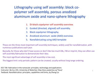
  • 1. Lithography using self assembly: block co- polymer self assembly, porous anodized aluminum oxide and nano-sphere lithography 1. Di-block copolymer self assembly overview. 2. Guided (directed, aligned) self assembly. 3. Block copolymer lithography. 4. Anodized aluminum oxide (AAO) overview. 5. Nanofabricating using AAO template Those are the three most important self-assembly techniques, widely used for nanofabrication, with numerous publications each year. Basically, for those who don’t have access or don’t like too much EBL, FIB or imprint, they can often use self-assembly fabrication to demonstrate their idea. The most significant advantage of self-assembly is low cost. The biggest limit: only periodic pattern can be created, usually without long range ordering. 1 ECE 730: Fabrication in the nanoscale: principles, technology and applications Instructor: Bo Cui, ECE, University of Waterloo; http://ece.uwaterloo.ca/~bcui/ Textbook: Nanofabrication: principles, capabilities and limits, by Zheng Cui
  • 2. a) A blend of two incompatible homo-polymer separates into distinct phases on a large scale (left), whereas block copolymers micro-phase separate into periodic domains (right). b) Basic morphologies obtained by different block copolymer compositions. Phase separation of block copolymers 1. A mixture of PMMA (Mw=93.9 kg/mol) and polystyrene (PS, Mw=194.9 kg/mol) (PS/PMMA=70/30, w/w) was dissolved in tetrahydrofuran (THF) to form a 5 wt% solution. 2. Polymer film was made by spin-cast the solution on glass slide. 3. Exposure to cyclohexane at 70oC to dissolve PS. Phase separation of a blend of PMMA and PS homo-polymer Ma, “Fabrication of super-hydrophobic film from PMMA with intrinsic water contact angle below 90o”, Polymer, 48, 7455-7460 (2007). PMMA, PS was dissolved 2
  • 3. “Nanochemistry: a chemical approach to nanomaterials” by Ozin Typical self assembly behavior for linear block copolymers 3
  • 4. Typical self assembly behavior for linear block copolymers 4 Block copolymer self-assembly study is started in the bulk phase, as shown above; whereas thin film is desired for nanofabrication and device application. When film thickness is well controlled, hole/pillar array or line array pattern can be created.
  • 5. TEM images of PS-PB diblock copolymer film masks (a,c) and lithographically patterned silicon nitride (b,d). One example: self-assembly of PS-PB di-block copolymer C. Harrison, Science The most attractive feature of block copolymer self assembly is the extremely high resolution, easily get features down to 10nm. PS: polystyrene PB: polybutadiene 5 Line array Pillar array
  • 6. Block copolymer thin films • Film applied by drop casting, dip coating, and spin coating. • Film is then treated to increase the degree of ordering. • Such as annealing above the order-disorder transition temperature for several days. • Or annealing at the presence of solvent vapor (toluene...) to swell the film and make the polymer more mobile. • One way to achieve alignment is through directional solidification strategy • Such as using a temperature gradient – the film is heated to above order-disorder transition and cooled in the presence of such gradient; so that the ordered phase nucleates at the cool end that serves as a template and orient the rest of the film. • Annealing film in the presence of a gradient in solvent vapor has similar effect. Film ordered by controlled solvent evaporation. Advanced Material, 16, 226 (2004) 6
  • 7. Synthesis: anionic living polymerization 7
  • 8. B A B A B A Block copolymer thin films: effect of substrate wetting Block A is shorter than B Arranged to minimize surface (interface) energy 8 (left) will result in line array (grating) pattern (right) will result in hole/pillar array pattern A forms cylinders embedded in B
  • 9. Lithography using self assembly: block co- polymer self assembly, porous anodized aluminum oxide and nano-sphere lithography 1. Di-block copolymer self assembly overview. 2. Guided (directed, aligned) self assembly. 3. Block copolymer lithography. 4. Anodized aluminum oxide (AAO) overview. 5. Nanofabricating using AAO template 9
  • 10. Micro-phase separated block copolymer can be directed/aligned by: • Electric field • Shearing force • Surface control of wettability • Chemical pattern on surface • Nano-structured surface • Spatial confinement by surface relief pattern in substrate and mold • Void in a range of porous host Guided block copolymer self assembly for long range ordering and periodicity 10
  • 11. Alignment by pre-patterning the substrate Spherical domains assembled from PS–PFS (polystyrene- polyferrocenyldimethylsilane) block copolymer inside patterned SiO2 grooves. The 1.5 wt.% PS-PFS block copolymer in toluene solution was spin-coated onto the grooved substrate and then annealed at 140oC for 48h to obtain a monolayer of spherical PFS domains in a PS matrix within the substrate grooves. Ross, “Templated self-assembly of block copolymers: effect of substrate topography”, Adv. Mater. 15, 1599–1602 (2003). 11
  • 12. Alignment by shear force (here for silicon nano-wire fabrication) Co-polymer on substrate Press Pull One way to create shear force. Here the etch contrast is increased by staining the block copolymer by 2 min exposure to the vapor from 0.5% aqueous RuO4, which selectively reacts with the PS block and increases its etch resistance, thus permitting Si nanowires of greater aspect ratio to be fabricated. a) Fabrication process for a Si nano-wire grid polarizer using block copolymer lithography. b) SEM image of the finished Si nano-wire grid on fused silica. 12
  • 13. Alignment by shear force (for silicon nano-wire fabrication) Pitch=30nm Tapping mode AFM phase images of PS–PHMA thin films on top of an -Si layer on a fused silica substrate: a) Quiescently annealed b) Shear aligned. Glassy (hard) PS cylinders are shown as light in a dark rubbery (soft) PHMA matrix. Polystyrene-b-poly(n-hexyl methacrylate) (PS– PHMA) diblock copolymer with a molar mass of 21 and 64 kg/mol for the respective blocks. Chaikin, “Silicon nanowire grid polarizer for very deep ultraviolet fabricated from a shear-aligned diblock copolymer template”, Optics letters, 32(21), 3125-3127 (2007). 13
  • 14. Templated self-assembly of block copolymers Polystyrene “brushes” by EUV-IL (interference lithography) and surface initiated nitroxide mediated living free radical polymerization The PS brush pitch should match that of PS-PMMA self assembly pitch. 14
  • 15. Polymerization of block-copolymers on chemically pre-patterned substrates P. F. Nealey, H. H. Solak et al. Nature 424 (2003) Polystyrene-block-methyl meth acrylate (PS-b-PMMA), L0 = 48nm Thermodynamics dominates interface widths and domain sizes. When Ls=47.5nmLo=48nm, block copolymer is almost defect free. 15 Here chemically patterned grating with polystyrene “brush”
  • 16. Block copolymer materials that naturally form simple periodic structures were directed to assemble into non-regular device oriented patterns (here an elbow) on chemically nano-patterned substrates. Mark P. Stoykovich, Marcus Müller,Sang Ouk Kim, Harun H. Solak, Paul F. Nealey, Science, 308, 1442-1446 (2005). Directed assembly of block copolymer blends into non-regular device oriented structure 16
  • 17. Directed assembly of nanoparticle filled block copolymer 17
  • 18. Alignment by electric field “Local control of microdomain orientation in diblock copolymer thin films with electric fields”, Science, 273, 931 (1996) 18
  • 19. Lithography using self assembly: block co- polymer self assembly, porous anodized aluminum oxide and nano-sphere lithography 1. Di-block copolymer self assembly overview. 2. Guided (directed, aligned) self assembly. 3. Block copolymer lithography. 4. Anodized aluminum oxide (AAO) overview. 5. Nanofabricating using AAO template 19
  • 20. Block copolymer lithography (add pattern transfer) PS: polystyrene PB: polybutadiene • Ozone breaks down PB’s C=C double bond. • OsO4 vapor reacts with PB’s double bond. Degrade with ozone Stain with OsO4 20 Os is a hard RIE mask
  • 21. Synthesis of nanowires by wetting a) Gold (or Ag) metal vapor- deposited onto a preformed PS- b-PMMA template. b) After annealing at 180°C for 1 min., gold nanoparticles segregate selectively to the PS domains and form chains. c) Repeated deposition and short- time annealing increases the metal loading, forming continuous conductive nanowires. Wettability masks: Au and Ag go to (“wet”) PS phase In, Pb, Sn go to PMMA phase Nature, 414, 735 (2001). 21
  • 22. Block copolymer lithography using PMMA-PS 1. After deep UV-exposure, polymer chain of PMMA is cut (PMMA is a positive deep UV lithography resist), making it more soluble in solvent. 2. Whereas the polystyrene (PS) chain is cross-linked, making it hard to dissolve by solvent. 3. Therefore, PMMA can be selectively removed by solvents like acetic acid afterwards. (PMMA chain can also be broken by UV light at =365nm, but need very long time exposure, 1 h at 40mW/cm2 intensity) 22
  • 23. Nanofabrication of vertical nanowires by electroplating • Aligned by electric field during annealing. • PS 71%, to obtain 14nm PMMA cylinder. • Deep UV simultaneously degrades PMMA and cross-link PS. • Acetic acid dissolve PMMA but not cross-linked PS (polystyrene). • Methanol is added to aqueous plating solution to better wet hydrophobic PS membrane. Science, 290, 2126 (2000) Electric field is for vertical alignment of self-assembly 23
  • 24. Density multiplication (here by 9) lithography A. Top-down and side-view schematics showing the arrangement of PS-b-PDMS block copolymer molecules in the region surrounding a single post made from cross-linked HSQ resist (by e-beam lithography). The post and substrate surfaces have been chemically functionalized by a monolayer of short-chain PDMS brush. B. A poorly ordered monolayer of BCP (block co-polymer) spherical domains formed on a flat surface ( without template guidance). The boundaries between different grain orientations are indicated with dashed lines. The inset is a 2D Fourier transform of the domain positions that shows the absence of long-range order. C-D. SEM images of ordered BCP spheres formed within a sparse 2D lattice of HSQ Ross, “Graphoepitaxy of self-assembled block copolymers on two-dimensional periodic patterned templates”, Science, 321, 939-943 (2008). For the moment, this is considered as the most promising route for bit-patterned magnetic recording media fabrication (make the mold for nanoimprint lithography), up to 10Tbits/in2 for pitch 8nm. 24
  • 25. Lithography using self assembly: block co- polymer self assembly, porous anodized aluminum oxide and nano-sphere lithography 1. Di-block copolymer self assembly overview. 2. Guided (directed, aligned) self assembly. 3. Block copolymer lithography. 4. Anodized aluminum oxide (AAO) overview. 5. Nanofabricating using AAO template 25
  • 26. 2Al + 3H2O → Al2O3 + 3H2 [G = -8.65  105J] Aluminum anodization setup Electrolyte: Oxalic acid, phosphoric acid, sulfuric acid … Anodization: • A direct current is passed through an electrolytic solution where the Al sheet is used as the anode. • Two processes: dissolving and oxidation • Naturally formed triangular pore arrays 26 Porous anodized aluminum Al2O3
  • 27. Porous Al2O3 membranes Top surface of the AAO Bottom surface of the AAO showing the barrier layer Cross section of the AAO AAO filter from Whatman Inc. 27
  • 28. Nano-pore formation mechanism • Two types of electrical current due to 1) oxide growth, 2) its dissolution. • The barrier has to be thin to be “transparent” for anions OH- and O2-. • These ions interacts with Al3+ ions, which can also move under electric field. • The wall is “pushed” upward by the continuous anodization at the oxide/Al interface. • Other mechanisms have also been reported. 28
  • 29. Schematic diagram of the pore formation at the beginning of the anodization. 1. Formation of barrier oxide on the entire area. 2. Local field distributions caused by surface fluctuations. 3. Creation of pores by field-enhanced or/and temperature-enhanced dissolution. Some pores stop growing due to competition among pores. 4. Stable pore growth. Nano-pore formation mechanism 29
  • 30. Pore dimensions Controlling parameters: voltage, electrolyte, temperature and time. Cell size D  2.5V (nm), V is voltage with a unit volt. Pore size d  V (nm), depends on pH; but pore can be enlarged in acids. 30
  • 31. Common acids for AAO Sulfuric acid generally gives smallest pore diameter and largest pore density. Standard deviation of pore diameter usually is within 10%. Oxalic acid 31
  • 32. Al2O3 Al AAO membrane production Wet-etch Al Etch barrier Commercial membrane: thickness 60m, pore size down to 20nm (one side only!) Application: filter, as template for nano-wire production. (using HgCl2) Free standing 10m-thick AAO membrane, with Au plated for better viewing contrast. 32
  • 33. • Removing Al without attacking AAO: saturated HgCl2 Al + HgCl2-----Al3+ + Hg, room temperature • Removing AAO without attacking Al: It is not easy for Al to dissolve in H2CrO4 aqueous. 6%H3PO4 + 1.8%H2CrO4, 60oC, 2h • Removing the barrier layer at the bottom without attacking too much the AAO pores. 5%H3PO4, 30oC, 30min Chemistry involved in nanofabrication using AAO 33
  • 34. Stages of the formation of self-ordered alumina: a) Annealing at 500oC for 3h to increase grain size; b) electro-polishing in a solution of 1/4 HClO4 + 3/4 C2H5OH for 4 min at 8V with agitation; c) first anodization; d) selective dissolution of the formed oxide layer; e) second anodization under the same conditions as the first anodization; and f) if needed, isotropic etching in 1M phosphoric acid at 30oC to widen the pores. Two-step anodization process to improve periodicity 34
  • 35. Pre-pattern Al surface can also improves periodicity Al is pre-patterned by FIB “Order–disorder transition of anodic alumina nanochannel arrays grown under the guidance of focused-ion-beam patterning”, page 2509-2511. 35
  • 36. Pre-pattern Al surface using imprint with a Ni mold Imprint pressure order 1000atm!! (regular imprint into resist 20atm) Schematic diagram of the fabrication of ideally ordered anodic alumina using Ni imprint stamps that can be replicated from: a) a resist pattern (method I). b) a silicon pattern (method II). Woo Lee, Ran Ji, Caroline A. Ross, Ulrich Gçsele, and Kornelius Nielsch, “Wafer-Scale Ni Imprint Stamps for Porous Alumina Membranes Based on Interference Lithography”, Small, 2006. 36
  • 37. Ideally ordered AAO by imprint pre-pattering Al SEM images of long-range-ordered anodic alumina with a) hexagonal and b) square arrangements of nano-pores. c,d) Oblique views of the cross sections. No other way can get such a high aspect ratio periodic pattern. AAO From same group, “Fast fabrication of long-range ordered porous alumina membranes by hard anodization”, Nature Materials, 2006. 37
  • 38. SEM of AAO with novel structure. (a) View of bottom, just removing the Al substrate in a mixed solution of HCl/CuCl2 (immersing for 20min); (b) extending the immersing time till 40 min, small pores appear; (c) extending the immersing time till 60 min; (d) after immersing in 5% H3PO4, the normal nano-pores are opened, surrounded by six small pores. The scale bar is 100nm. HCl/CuCl2 40min Open in H3PO4 d b a c HCl/CuCl2 60min Shiyong Zhao, Arthur Yelon and Teodor Veres. “Novel structure of AAO film fabricated by constant current anodization” Adv. Mater. 19(19), 3004, 2007. Novel structure of AAO film Anodization using 0.8 M H2SO4 + 0.1 M Al2(SO4)3 solution. Addition of Al2(SO4)3 allows higher current density/voltage, which leads to this new structure. A discovery by “accident”. 38
  • 39. Lithography using self assembly: block co- polymer self assembly, porous anodized aluminum oxide and nano-sphere lithography 1. Di-block copolymer self assembly overview. 2. Guided (directed, aligned) self assembly. 3. Block copolymer lithography. 4. Anodized aluminum oxide (AAO) overview. 5. Nanofabricating using AAO template. 39
  • 40. Shrink pore diameter by isotropic coating onto AAO Z. Ye, H. Liu, I. Schultz, W. Wu, D. G Naugleand I. Lyuksyutov, Nanotechnology 19, 325303 (2008). Au electrode TiO2 is coated by isotropic sol–gel deposition technique Co nanowires in TiO2 nanotubes • The pore spacing and the pore diameter are coupled to each other and determined by the applied voltage of anodization. • Pores are easy to enlarge using subsequent wet etching after anodization. • It is more challenging to shrink the pore size. 40
  • 41. Bare AAO TiO2 nanotubes after dissolving AAO AAO coated with TiO2 Cross section of TiO2 nanotubes Recipe: TiF4+ H2O → TiO2+ HF at 60oC and pH = 2 Deposition of TiO2 nanotubes using Sol-Gel method 41
  • 42. Electroplating of nanowires Aspect ratio: 50μm/60nm 800 This extremely high aspect ratio is hard to achieve by lithography plus etching 42
  • 43. Other nanofabrication routes using AAO VLS: vapor-liquid-solid method for nano-wire growth, see http://en.wikipedia.org/wiki/Vapor-liquid-solid_method 43
  • 44. Nano-pore array in GaN by RIE using AAO as mask Nano-pillar array in GaN by metal liftoff using AAO, followed by GaN RIE. Patterning GaN using AAO 44
  • 45. Grow carbon nanotube into AAO pores 45
  • 46. Nanotubular super-capacitor for energy storage MIM: metal-insulator-metal here TiN (“metal”), Al2O3 and TiN, all deposited by atomic layer deposition (ALD). Due to the enormous interface area, the capacitance is huge (C  area), with peak (discharge) power up to 106 W/kg. Energy stored = ½ CV2  C. “Nanotubular metal–insulator–metal capacitor arrays for energy storage”, Nature Nanotechnology, 2009. 46
  • 47. • Al foils are interesting but limited. It is not microfabrication compatible. • Al films on wafers are. AAO on flat surface may be used for data storage with high density. AAO on wafers Only 300nm Al 47
  • 48. Magneto-optics of Ni nanowires Nanotechnology 17 5764 (2006) Pitch 70nm Challenges for AAO using thin Al film: • The deposited Al is usually not as pure as Al sheet due to oxidization or (cross-) contamination during film deposition. (Al atom is so reactive) • Al film is usually too thin for two-step anodization, thus poor periodicity. • Electrochemical polish would also be extremely difficult to control for thin films. 48
  • 49. M. Dresselhaus, MIT Thicker alumina templates on silicon wafers Al is thicker here, for polishing 49
  • 50. Nano-wire by alumina template (results using the steps in previous slide) Pore oblique view Cross-section (100nm) Filled with nano-wire 50 Here Al film is >2m. Some pores are not filled by metal
  • 51. 51