Download to read offline

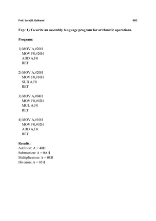
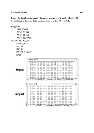
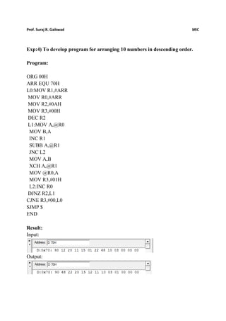
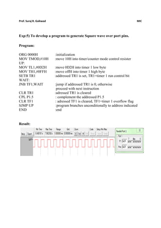
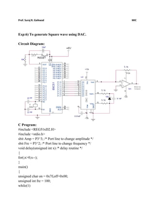
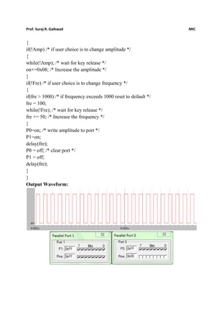
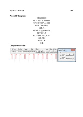
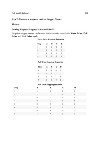
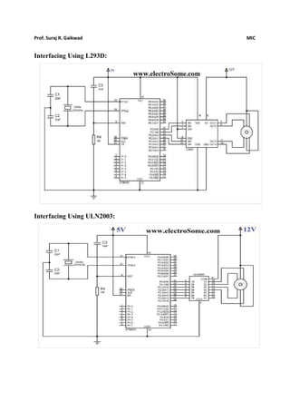
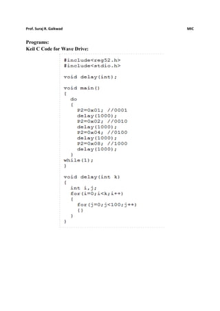

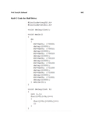
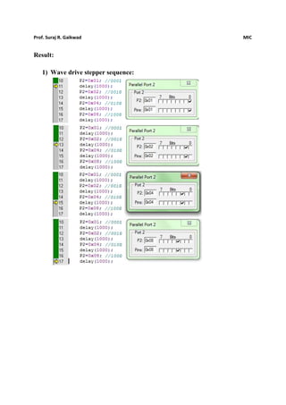
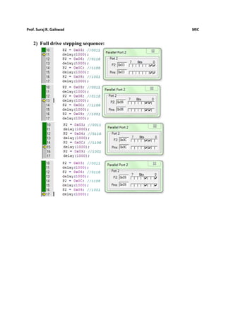
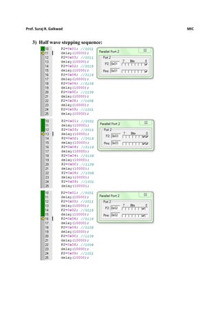
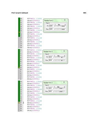
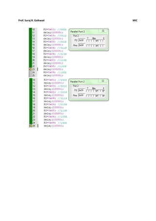
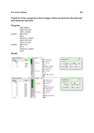
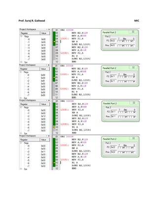

This document contains the description of 9 experiments conducted using an 8051 microcontroller. The experiments include writing assembly programs for arithmetic operations, memory block transfer, number squaring, arranging numbers in descending order, generating square waves using timers and DAC, driving a stepper motor, and reading a keyboard to display codes on a seven segment display. Assembly and C code are provided for the various experiments. The results of each experiment are also shown.


![[Báo cáo] Bài tập lớn Xử lý tín hiệu số: Thiết kế bộ lọc FIR](https://cdn.slidesharecdn.com/ss_thumbnails/btlxulyso-150904175424-lva1-app6892-thumbnail.jpg?width=640&height=640&fit=bounds)
![[Cntt] bài giảng kĩ thuật vi xử lí](https://cdn.slidesharecdn.com/ss_thumbnails/cnttbigingkthutvixl-160829131326-thumbnail.jpg?width=640&height=640&fit=bounds)


![[Deck] What's New in Spark-Iceberg Integration via DSV2.pptx](https://cdn.slidesharecdn.com/ss_thumbnails/deckwhatsnewinspark-icebergintegrationviadsv2-260210005337-25955b12-thumbnail.jpg?width=640&height=640&fit=bounds)


