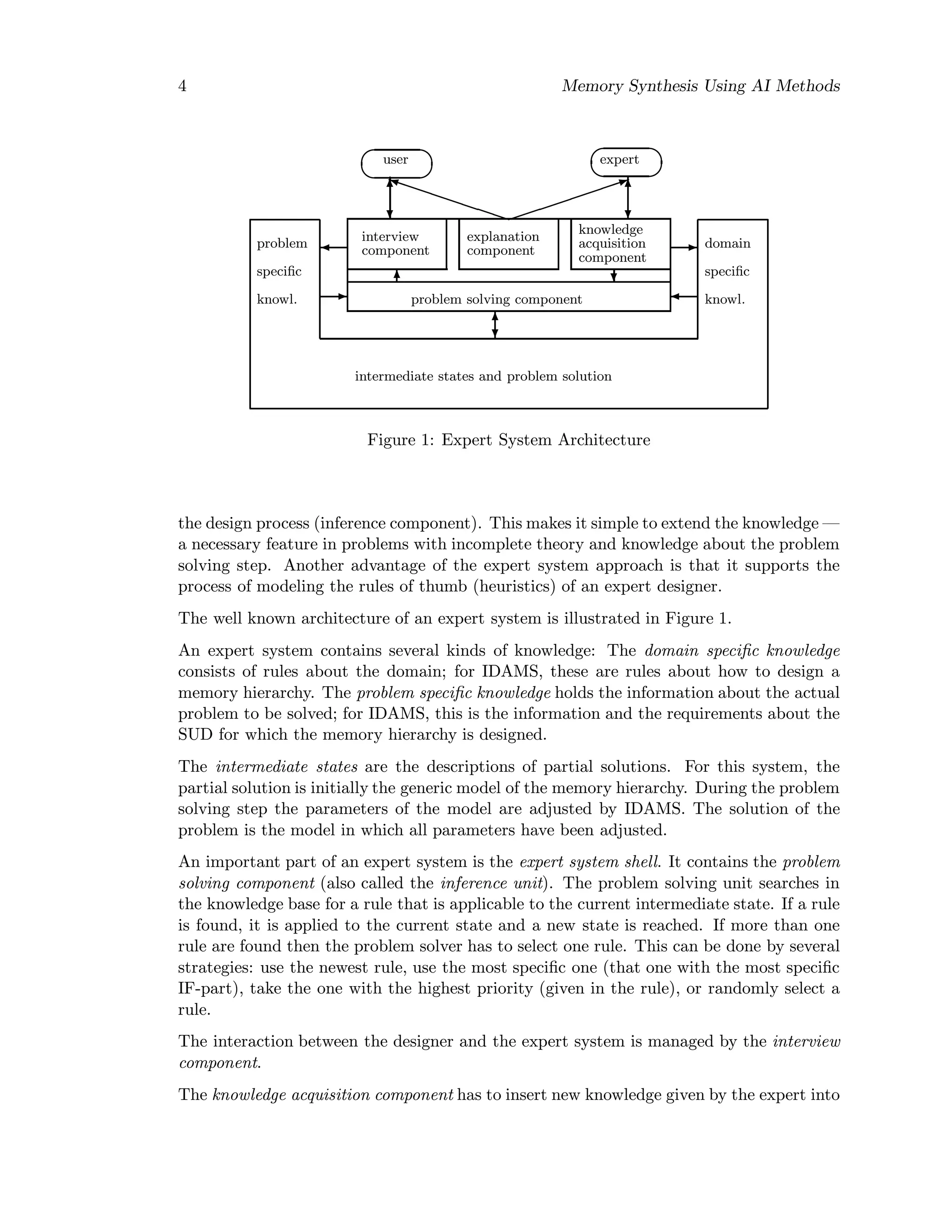
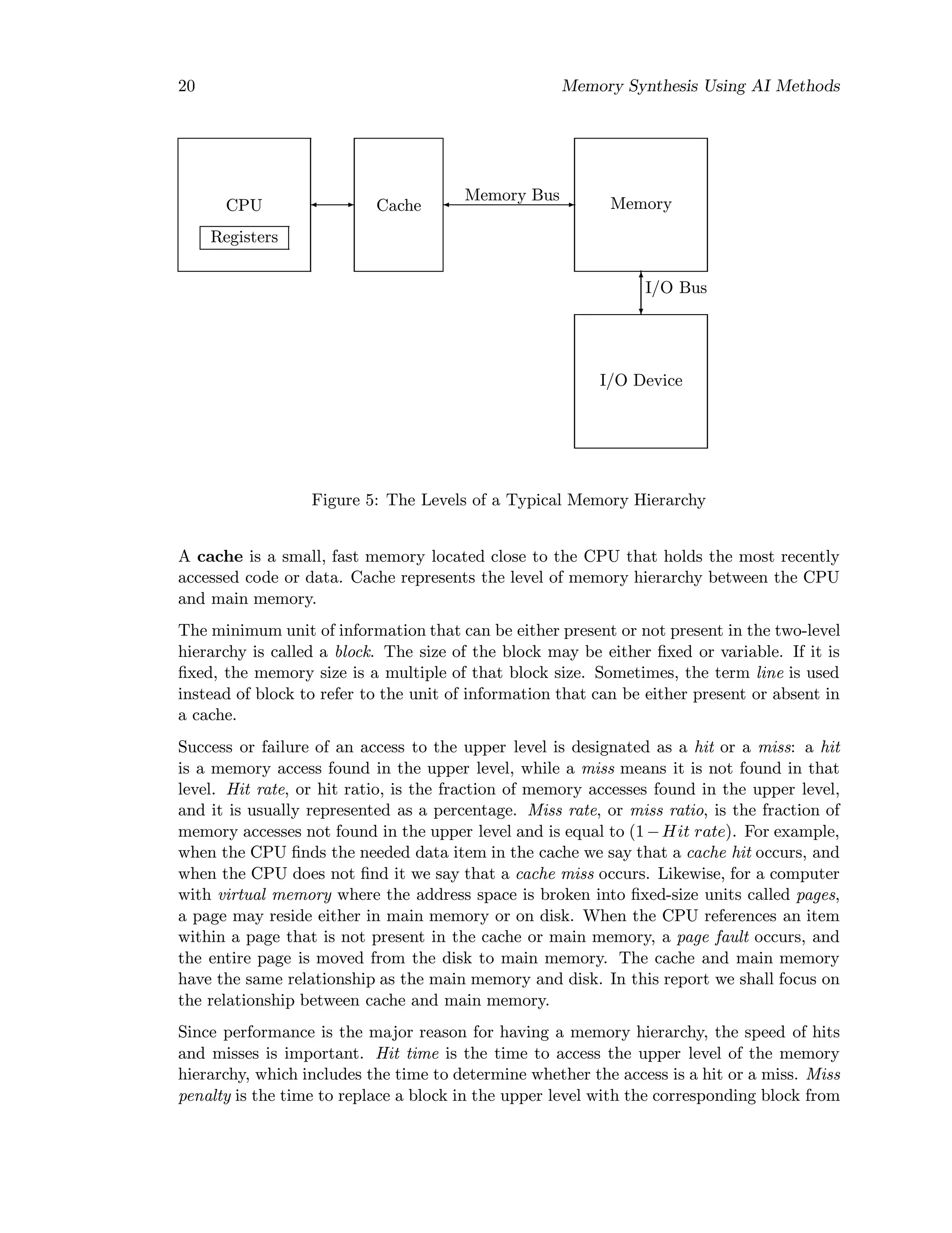
Download to read offline

![12 Memory Synthesis Using AI Methods
4 COMPUTER ARCHITECTURE OVERVIEW
4.1 An Architecure Classification
Designing a computer system is a task having many aspects, including instruction set de-
sign, functional organization, logic design, and implementation. The design of the machine
should be optimized across these levels. The term instruction set architecture refers to the
actual programmer-visible instruction set. The instruction set architecture serves as the
boundary between the hardware and the software. The term organization includes the
high-level aspects of a computer’s design, such as the memory system, the bus structure,
and the internal CPU design. Hardware is used to refer to the specifics of a machine, such
as the detailed logic design and the packaging technology of the machine. Hardware is
actually the main aspect of implementation, which encompasses integrated circuit design,
packaging, power, and cooling. We shall use the term architecture to cover all three aspects
of computer design.
According to the number of processors included, computer systems fall into two broad
categories: uniprocessor computers —which contain only one CPU—, and multiprocessor
computers —which contain more CPU’s. The CPU can be partitioned into into three
functional units, the instruction unit (also called the control unit) (I-unit), the execution
unit (E-unit), and the storage unit (S-unit);
• the I-unit is responsible for instruction fetch and decode and generates the control
signals; it may contain some local buffers for instruction prefetch (lookahead);
• the E-unit executes the instructions and contains the logic for arithmetic and logical
operations (the data path blocks);
• the S-unit provides the memory interface between the I-unit and the E-unit; it
provides memory management (protection, virtual address translation) and may
contain some additional components whose goal is to reduce the access time to data.
A finer classification of computer architectures may be made taking into account not only
the number of CPU’s but also the instruction and data flow. Under this approach, there
are three architectures ([7]):
• Single Instruction Stream Single Data Stream (SISD) architecture, in which a single
instruction stream is executed on a single stream of operands;
• Single Instruction Stream Multiple Data Stream (SIMD) architecture, in which a
single instruction stream is executed on several streams of operands;
• Multiple Instruction Stream Multiple Data Stream (MIMD) architecture, in which
different instruction streams are executed on different operand streams in parallel.
In this report we shall use as synonym for the MIMD architecture the term multiprocessor.
Multiprocesing is a way to increase system computing power. A distinctive feature of an](https://image.slidesharecdn.com/memorysynthesisusingaimethods-201006184613/75/Memory-synthesis-using_ai_methods-18-2048.jpg)
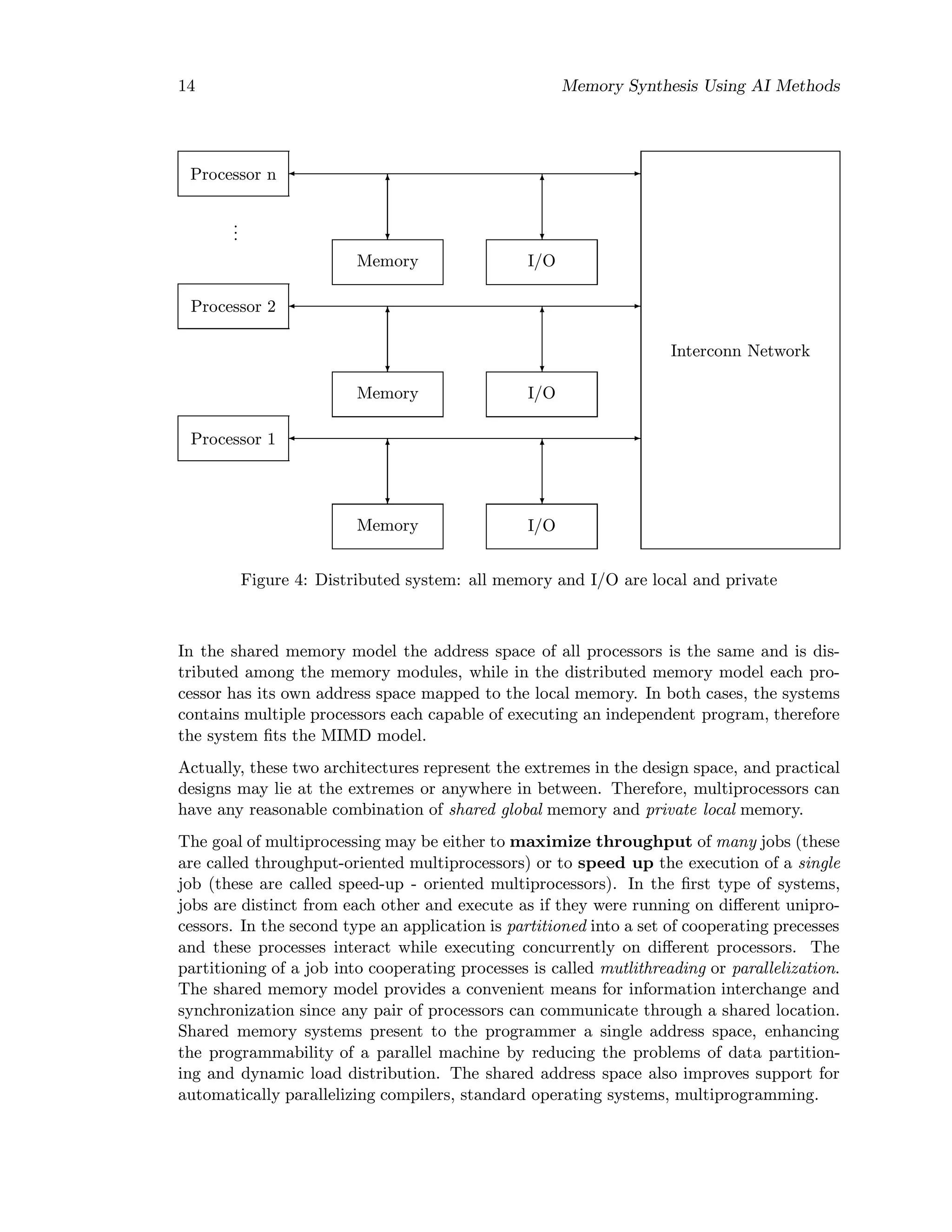
![Memory Synthesis Using AI Methods 13
Processor 1
Processor 2
...
Processor n
Interconn Network
Memory
Memory
...
Memory
I/O
I/O
Figure 3: Shared-memory system: all memory and I/O are remote and shared
MIMD architecture is that multiple instruction streams must communicate or synchronize
by passing message or sharing memory.
4.2 Multiprocessors
Among multiprocessors, we can distinguish two broad classes, according to the logical
architecture of their memory systems [7]:
• shared memory systems (also called tightly coupled systems): all processors access
a single address space (Figure 3).
• distributed systems (also called loosely coupled systems or multicomputers) : each
processor can access only its own memory; each processor’s memory is logically
disjoint from other processor’s memory (Figure 4). In order to communicate, the
processors are sending messages to each other.
A memory unit is called a memoru module. Each processor has registers, arithmetic and
logic units, and access to memory and input/output modules. The distinction between
the architectures stems from way memory and input/output units are accessed by the
processor:
• in the shared memory model, memory and I/O systems are separate subsystems
shared among all of the processors;
• in the distributed memory model, memory and I/O units are attached to individual
processors; no sharing of memory and input/output is permitted.](https://image.slidesharecdn.com/memorysynthesisusingaimethods-201006184613/75/Memory-synthesis-using_ai_methods-19-2048.jpg)
![Memory Synthesis Using AI Methods 15
The distributed system (i.e., local and private memory and I/O) supports communication
through point-to-point exchange of information, usually by message passing.
Depending on the structure of the interconnection network, there are two types of shared-
memory architectures:
• bus-based memory systems: the memory and all processors (with optional private
caches) are connected to a common bus. In other words, communication on a bus
is of broadcast type: any memory access made by one CPU can be “seen” by all
CPU’s.
• general interconnection networks: they provide several simultaneous connections
between pairs of nodes, that is, only two nodes are involved in any connection: the
sender and the receiver. These interconnection networks adhere to the point-to-point
communication model and may be direct or multistage networks.
4.3 Multiprocessing performance
The main purpose of a multiprocessor is either to increase the throughput or to decrease
the execution time, and this is done by using several machines concurrently instead of
a single copy of the same machine. In some applications, the main purpose for using
multiple processors is for reliability rather than high performance; the idea is that if any
single processor fails, its workload can be performed by other processors in the system
(fault-tolerant computing). The design principles for fault-tolerant computers are quite
different from the principles that guide the design of high-performance systems. We shall
focus our attention on performance.
As mentioned in Section 3.2, the amount of overall Speedup is dependent on the fraction of
time that a given enhancement is actually used. In the case of improving performance by
using multiprocessing instead of uniprocessing, the overall efficiency is maximum when all
processors are engaged in useful work, no processor is idle, and no processor is executing
an instruction that would not be executed if the same algorithm were executing on a
single processor. This is the state of peak performance, when all N processors of a
multiprocessor are contributing to effective performance, and in this case the Speedup is
equal to N. Peak performance is rarely achievable because there are several factors ([7])
that introduce inefficiency, such as:
• the delays introduced by interprocessor communications;
• the overhead in synchronizing the work of one processor with another;
• lost efficiency when one or more processors run out of tasks;
• lost efficiency due to wasted effort by one or more processors;
• the processing costs for controlling the system and scheduling operations.](https://image.slidesharecdn.com/memorysynthesisusingaimethods-201006184613/75/Memory-synthesis-using_ai_methods-21-2048.jpg)
![Memory Synthesis Using AI Methods 17
1. hardware level synchronization primitives such as TEST&SET(lock),
RESET(lock), FETCH&ADD(x,a), Empty/Full bit;
2. software-level synchronization mechanisms such as semaphores and barriers;
• message passing; This method can be used both for shared memory and distributed
systems.
Synchronization mechanisms are used to provide mutual exclusive access to shared variable
and to coordonate the execution of several processes:
Mutual exclusive access
Acces is mutually exclusive if no two processes access a shared variable simultaneously.
A critical section is an instruction sequence that has mutually exclusive access to shared
variables. Locks and semaphores can be used to guarantee mutual exclusive access. On a
uniprocessor, mutual exclusion can be guaranteed by disabling interrupts.
Conditional synchronization
Conditional synchronization is a method of process coordination which ensures that a set
of variables are in a specific state (condition) before any process requiring that condition
can proceed. Mechanisms such as Empty/Full bit, Fetch&Add, and Barrier can be used
to synchronize processes.
4.5 Coherence, Consistency, and Event Ordering
Memory coherence is a system’s ability to execute memory operation corectly. We need a
precise definition of correct execution. Censier and Feautrier define [1] a coherent memory
system as follows:
A memory scheme is coherent if the value returned on a LOAD opera-
tion is always the value given by the latest STORE operation with the
same address.
This definition, while very concise and intuitive, is difficult to interpret and too ambiguous
in the context of a multiprocessor, in which data accesses may be buffered and may not
be atomic.
An access by processor i on a variable X is called atomic if no other processor is allowed
to access any copy of X while the access by processor i is in progress.
A LOAD of a variable X s said to be performed at a point in time when issuing of a STORE
from any processor to the same address cannot affect the value returned by the LOAD.
A STORE on a variable X by processor i is said to be performed at a point in time when an
issued LOAD from any processor to the same address cannot return a value of X preceding
the STORE.
Accesses are buffered if multiple accesses can be queued before reaching their destination,
such as main memory or caches.](https://image.slidesharecdn.com/memorysynthesisusingaimethods-201006184613/75/Memory-synthesis-using_ai_methods-23-2048.jpg)
![Memory Synthesis Using AI Methods 31
This simple model of miss causes has some limits. For example, increasing cache size re-
duces capacity misses as well as conflict misses, since a larger cache spreads out references.
Thus, a miss might move from one category to the other as parameters change.
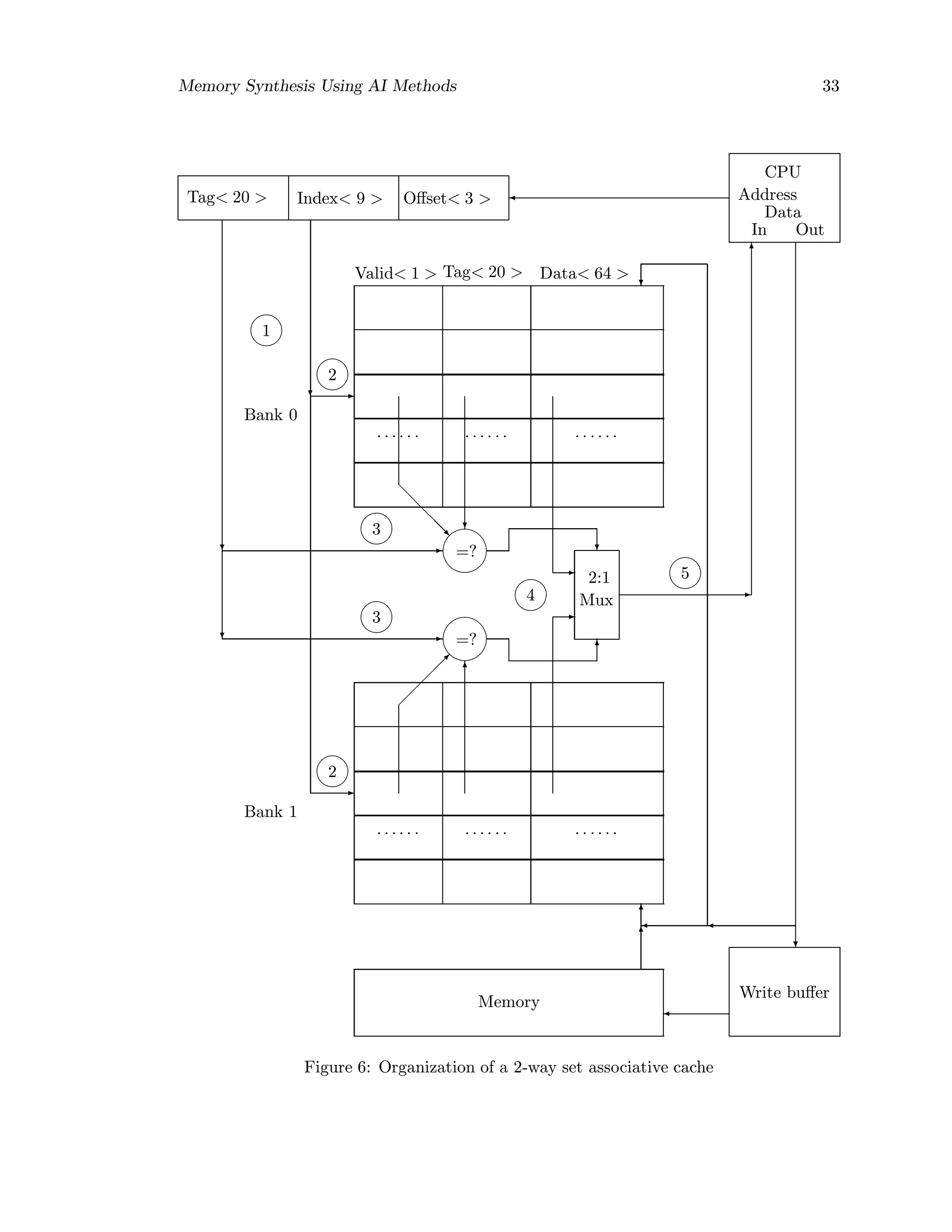
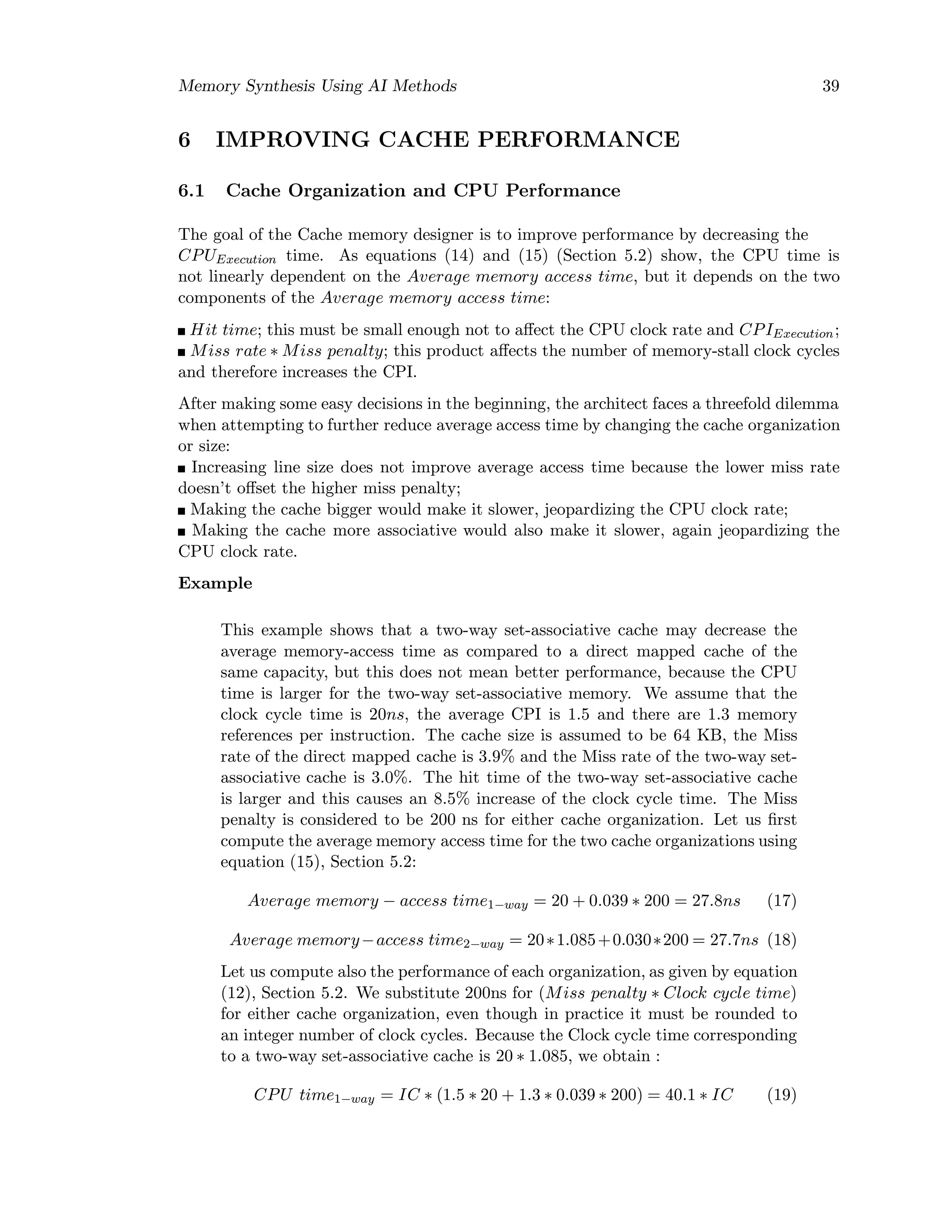
5.9 Line Size Impact on Average Memory-access Time
Let us analize the effect of the block size on the Average memory−access time (equation
(15), Section 5.2) by examining the effect of the line size on the Miss rate and Miss penalty.
We assume that the size of the cache is constant.
Larger block sizes reduce compulsory misses, as the principle of spatial locality suggests.
At the same time, larger block sizes increase conflict misses, because they reduce the
number of blocks in the cache. Reasoning in terms of the two aspects of the principle of
locality, we say that increasing line size lowers the miss rate until the reduced misses of
larger blocks (spatial locality) are outweighted by the increased misses as the number of
blocks shrinks (temporal locality), because larger block sizes means fewer blocks in cache.
Let us examine the effect of line size on the Miss penalty. The Miss penalty is the sum of the
access latency and the transfer time. The access-latency portion of the miss penalty is not
affected by the block size, but the transfer time does increase linearly with the block size.
If the access latency is large, initially there will be little additional miss penalty relative
to access time as block size increases. However, increasing the line size will eventuaslly
make the transfer-time become an important part of the miss penalty.
Since a memory hierarchy must reduce the Average memory-access time, we are interested
not in the lowest Miss rate, but in the lowest Average access time. This is related to
the product of Miss rate by the Miss penalty, according to equation (15), Section 5.2.
Therefore, the “best” line size is not that which minimizes Miss rate, but that which
minimizes the product between the Miss rate and the Miss penalty. Measurements on
different cache organizations and computer architectures have indicated that the lowest
average memory-access time is for line sizes ranging from 8 to 64-bytes ([6],[20]).
Of course, overall CPU performance is the ultimate performance test, so care must be taken
when reducing Average memory-access time to be sure that changes to Clock cycle time
and CPI improve overall performance as well as average memory-access time.
5.10 Operating System and Task Switch Impact on Miss Rate
When the Miss rate for a user program is analized (for example, by using a trace-driven
simulation), one should take into account that the real miss rate for a running program,
including the operating system code invoked by the program, is higher. The miss rate can
be broken into three components:
• the miss rate caused by the user program;
• the miss rate caused by the operating system code;
• the miss rate caused by the conflicts between the user code and the system code.](https://image.slidesharecdn.com/memorysynthesisusingaimethods-201006184613/75/Memory-synthesis-using_ai_methods-37-2048.jpg)
![38 Memory Synthesis Using AI Methods
memory.
With respect to the second type of failure —associated with program migration—, let us
suppose that processor P1 is running a program that leaves in the cache the value 0 for
variable X. Then the program shifts to a different processor P2 and writes a new value
of 1 for variable X in the cache of that processor. Finally, the program shifts back to
processor P1 and attempts to read the current value of X. It obtains the old, stale value
of 0 when it should have obtained the new, fresh value 1 for X. Note that X does not
have to be a shared variable for this type of error to occur. The cause of this mode of
failure is ([7]) that a program’s footprint —that is, data associated with the program—
was not flushed completely from cache when the program has moved from P1 to P2 and
when it got back to P1 it has found there stale data.
The protocols that maintain cache coherence for multiple processors are called cache-
coherence protocols. This subject has been studied by many authors, among them being
Censier and Feautrier ([1]), Dubois and Briggs ([3],[4]), Archibald and Baer ([5]), Agarwal
([10]), Lenovski, Laudon, Garachorloo, Gupta and Hennessy ([17]), who have explored a
variety of cache-coherence protocols and examined their performance impact. Chapter 9
covers issues related to cache coherence. The implementation of cache in multiprocessors
may enforce coherence either totally by the hardware, or may enforce coherence only at
explicit synchronization points.
5.14 Cache Flushing
When a processor invalidates data in its cache, this is called flushing or purging. Sometimes
(Sections 5.13.1 and 9.6), it is necessary to invalidate the contents of more lines in cache,
i.e., to set the invalid bit for more lines. If this is done one line at time, the required time
would become excessive. Therefore, an INVALIDATE instruction should be available in the
processor if a coherence scheme based on flushing is used. If one chooses to flush the entire
cache, then resettable static random-access memories for Valid bits can be used allowing
the INVALIDATE to be accomplished in one or two clocks.](https://image.slidesharecdn.com/memorysynthesisusingaimethods-201006184613/75/Memory-synthesis-using_ai_methods-44-2048.jpg)
![Memory Synthesis Using AI Methods 41
if one copy is modified, the other will have the wrong value. Hardware schemes, called
anti-aliasing, that guarantee every cache line a unique physical address may be employed
to solve this problem, but software solution are less expensive. The idea of the software
solution is to force aliases to share a number of address bits so that the cache can not
accomodate duplicates of aliases. For example, for a direct mapped cache that is 256 KB,
that is 218KB, and if the operating system enforces that all aliases are identical in the last
18 bits of their addresses, then no two aliases can be simultaneously in cache. The third
problem is that I/O typically uses physical addresses and thus requires mapping to virtual
addresses to interact with a virtual cache in order to maintain coherence.
6.3 Reducing Read Miss Penalty
Because reads dominate cache accesses. it is important to make read misses fast. There
are several methods to reduce the read miss penalty. In the first method, called fetch
bypass or out-of-order fetch, the missed word is requested first, regardless of its position
in the line, data requested from memory is transmitted in parallel to the CPU and cache,
and the CPU waits only for the requested data, while in the second method, called early
restart, the line that contains the requested data is brought from memory starting with
the left-most byte, but the CPU continues execution as soon as the requested data arrives.
With fetch bypass, the missed word is requested first from memory and sent to the CPU as
soon as it arrives, bypassing the cache; the CPU continues execution while filling the rest
of the words in the block. Because the first word requested by the CPU may not be the
first word of a line, this strategy is also called out-of-order fetch or wrapped fetch. Usually,
the cache is loaded in parallel when the processor reads data from main memory (i.e., fetch
bypass with simultaneous cache fetch) in order to overlap fetching of the specified data for
CPU and for cache. When the transfer begins with a byte that is not the left-most byte
of the line, the transfer should wrap around the right-most byte of the line and transfer
the left-most bytes of the line that have been skipped in the first place.
This methods provide a reduction of the read miss penalty by obviating the need for the
processor to wait for the cache to load the entire line. Unfortunately, not all the words of
a line have an equal likelihood of being accessed first. If that were true, with a line size
of L bytes, the average line entry point would be L/2. However, due to sequential access,
the left side of the line is more likely to be accessed first. For example, Hennessy and
Patterson have determined [6] for some architecture that the average line entry point for
instruction fetch is at 5.6 bytes from the left-most byte in a 32-byte line. The left-word
of a block is most likely to be accessed first due to sequential accesses from prior blocks
on instruction fetches and sequentially stepping through arrays for data accesses. This
effect of spatial locality limits the performance improvement obtained with out-of-order
fetch. Spatial locality also affects the efficiency of early restart, because it is likely that the
next cache request be to the same line. The reduction in the read miss penalty obtained
with these methods should be compared to the increased complexity incurred by handling
another request while the rest of one line is being filled.](https://image.slidesharecdn.com/memorysynthesisusingaimethods-201006184613/75/Memory-synthesis-using_ai_methods-47-2048.jpg)
![42 Memory Synthesis Using AI Methods
6.4 Reducing Conflict Misses in a Direct-Mapped Cache
As described in Section 5.8, conflict misses may appear when two addresses map into the
same cache set. Consider referencing a cache with two addresses, ai and aj. Using the bit
selection method described in Section 5.4, these two addresses will map into the same set
if and only if they have identical Index fields. Denoting by b the bit selection operation
performed on the addresses to obtain the index, then the two addresses will map into the
same set iff:
b[ai] = b[aj] (23)
Two addresses that satisfy this equation are called conflicting addresses because they may
potentially cause conflicts. Assume the following access pattern:
ai aj ai aj ai aj ai aj . . .
where addresses ai and aj are conflicting addresses. A 2-way set-associative cache will not
suffer a miss if the processor issues this adddress pattern because data referenced by ai
and aj can co-reside in a set. In contrast, in a direct-mapped cache, the reference to aj
will result in an interference (or conflict) miss because the data from ai occupies the same
selected line.
The percentage of misses that are due to conflicts varies widely among different applica-
tions, but it is often a substantial portion of the overall miss rate.
6.4.1 Victim Cache
The victim cache scheme has been proposed by Jouppi [12]. A victim cache is a small,
fully-associative cache that provides some extra cache lines for data removed from the the
direct-mapped cache due to misses. Thus, for a reference stream of conflicting addresses,
such as
ai aj ai aj ai aj ai aj . . .,
the second reference, aj, will miss and force the data indexed by ai out of the set. The
data that is forced out is placed in the victim cache. Consequently, the third reference, ai,
will not require accessing the main memory because the data can be found in the victim
cache. Fetching a conflicting datum with this scheme requires two or three clock cycles:
1. the first clock cycle is needed to check the primary cache;
2. the second cycle is needed to check the victim cache;
3. a third cycle may be needed to swap the data in the primary cache and victim cache
so that the next access will likely find data in the primary cache;
This scheme has several disadvantages: it requires a separate, fully-associative cache to
store the conflicting data. Not only does the victim cache consume extra area, but it can
also be quite slow due to the need for an associative search and for the logic to maintain a
least-recently-used replacement policy. For adequate performance a sizeable victim cache
is required in order for the victim cache to be able to store all conflicting data blocks. If
the size of the victim cache is fixed relative to the primary direct-mapped cache, then it
is not very effective at resolving conflicts for large primary caches.](https://image.slidesharecdn.com/memorysynthesisusingaimethods-201006184613/75/Memory-synthesis-using_ai_methods-48-2048.jpg)
![Memory Synthesis Using AI Methods 43
6.4.2 Column-Associative Cache
The challenge is to find a scheme that minimizes the conflicts that arise in direct-mapped
accesses by allowing conflicting addresses to dynamically choose alternate mapping func-
tions, so that most of the conflicting data can reside in the cache. At the same time,
however, the critical hit access path (which is an advantage of direct-mapped organiza-
tion) must remain unchanged. The method presented is called Column-Associativity and
has been invented by A. Agarwal and S.D. Pudar [11].
The idea is to emulate a 2-way set-associative cache with a direct-mapped cache by map-
ping two conflicting addresses to different sets instead of referencing another line in the
same set as the 2-way set-associativity does. Therefore, conflicts are not resolved within
a set but within the entire cache, which can be thought of as a column of sets —thus the
name column associativity. The method uses two mapping functions (also called hashing
functions) to access the cache. The first hashing function is the common bit selection,
that is, an address ai is mapped into the set with the number:
b[ai] (24)
The second hashing function is a modified bit-selection, which gives the same value as
the bit-selection function except for the highest-order bit, which is inverted. We call this
hashing function bit flipping and denote it by f. For example, if b[a] = 010, then applying
the bit flipping function to the address a yields f[a] = 110. Therefore, the function f
applied to an address aj will always give a set number which is different from that given
by the function b:
b[aj] = f[aj] (25)
The scheme works as follows:
1. the bit selection function b is applied to a memory address ai. If b[ai] indexes to
valid data, a first-time hit ocurs, and there is no time penalty;
2. if the first access has missed, then the bit flipping function f is used to access the
cache. If f[ai] indexes to valid data, then a second-time hit occurs and data is
retrieved.
3. if a second-time hit has occured, then the two cache lines are swapped so that the
next access will likely result in a first-time hit.
4. if the second access misses, then data is retrieved from main memory, placed in the
cache set indexed by f[ai], then it is swapped with the data indexed by b[ai] with
the goal of making the next access likely to be a first-time hit.
The first and second step each require one clock cycle, while swapping requires two clock
cycles. The second-time hit, including swapping, is then four cycles but can be reduced
to only three cycles using an extra buffer for the cache: Given this buffer, the swap need
not involve the processor, which may be able to do other useful work while waiting for the
cache to become available again. If this is the case half of the time, then the time wasted](https://image.slidesharecdn.com/memorysynthesisusingaimethods-201006184613/75/Memory-synthesis-using_ai_methods-49-2048.jpg)
![44 Memory Synthesis Using AI Methods
by a swap is only one cycle. Therefore, it can be considered that a swap adds only one
cycle to the execution time, and hence the second-time hit is 3 clock cycles.
Using two hashing functions mimics 2-way set-associativity because for two conflicting
addresses, ai and aj, rehashing aj with f resolves the conflict with a high probability: from
equations (23) and (25) it results that the function f applied to aj will give a set different
from b[ai]:
b[ai] = b[aj] = f[aj] (26)
The difference is that a second-time hit takes three clock cycles, while in a 2-way set-
associative cache the two lines of a set can be retrieved in a clock cycle. However, the
clock cycle of the two-way set-associative cache is longer that the clock cycle of the direct-
mapped cache.
A problem that must be solved for column-associative caches is the problem of possible
incorrect hits. Consider two addresses, ai and ak, that map with bit-selection to indexes
that differ only in the highest-order bit. In this case, the index obtained by applying bit-
selection mapping to one address is the same as the index obtained by applying bit-flipping
mapping to the other address:
b[ak] = f[ai] and b[ai] = f[ak] (27)
These two addresses are distinct, but they may have identical tag fields. If this is the case,
when a rehash occurs for the address ai and data addressed by ak is already in cache at
location b[ak], then the bit-flipping mapping f[ai] results in a hit with a data block that
should only be accessed by b[ak]. For example, if
b[ak] = 110, b[ai] = 010, and Tag[ak] = Tag[ai] (28)
and assuming that data line addressed by ak is cached in the set with the index b[ak], then
when the address ai is presented to the cache, this address will be rehashed to the same
set as ak (i.e., f[ai] = 110) and will cause a second-time hit (a false hit) because the two
addresses have the same Tag. This is incorrect, because a data-line must have a one-to-one
correspondence with a unique memory address. The solution to this problem is to extend
the Tag with the highest-order bit of the index field. In this case, the rehash with f[ai]
will correctly fail because information about ai and ak having different indexes is present
in the Tag. In this way, the data line stored in the set with the number b[ak] = f[ai] is
put into correspondece with an unique index, and hence a unique address.
Another problem is that storing conflicting data in another set is likely to result in the
loss of useful data, and this is referred to as clobbering. The source of this problem
is that a rehash is attempted after every first-time miss, which can replace potentially
useful data in the rehashed location, even when the primary location had an inactive
line. Clobbering may lead to an effect called secondary thrashing that is presented in the
following paragraph.
Consider the following reference pattern:
ai aj ak aj ak aj ak . . . ,
where the addresses ai and aj map into the same cache location with bit selection, and ak](https://image.slidesharecdn.com/memorysynthesisusingaimethods-201006184613/75/Memory-synthesis-using_ai_methods-50-2048.jpg)
![Memory Synthesis Using AI Methods 45
is an address which maps into the same location with bit-flipping, that is:
b[ai] = b[aj], b[ak] = f[ai] and f[ak] = b[ai] (29)
After the first two references, the data referenced by aj (which will be called j for brevity)
and the data i will be in the non-hashed and rehashed locations, respectively (because of
swapping). When the next address, ak, is encountered, the algorithm attempts to access
b[ak] (bit selection is tried first), which contains the rehashed data i; when the first-time
miss ocurs, the algorithm tries to access f[ak] (bit flipping is tried second), which results
in a second-time miss and the clobbering of the data j. This pattern continues as long
as aj and ak alternate: the data referenced by one of them is clobbered as the inactive
data block i is swapped back and forth but never replaced. This effect is referred to as
secondary thrashing.
The solution to this problem is finding a method to inhibit a rehash access if the location
reached by the first-time access itself contains a rehashed data block, that is, with the
previous notation, when the location referenced by ak with bit-selection (b[ak]) already
contains a rehashed data (data i is rehashed to f[ai]). This condition can be satisfied by
adding to each cache set an extra bit that indicates whether the set is a rehashed location,
that is, whether the data in that set is indexed by f[a]. This bit that indicates a rehashed
location is called the rehash bit, denoted by Rbit, and it makes possible to test if a first-
time miss occurs on a rehashed data and thus to avoid rehashing a first-time miss to a
set that contains rehashed data. Therefore, the scheme for column associativity is the
following (step 2 of the the basic scheme is modified to avoid clobbering):
1. the bit-selection hashing function b is applied to a memory address a. If b[a] indexes
to valid data, a first-time hit ocurs, and there is no time penalty;
2. if the first access is a miss, then the action taken depends on the value of the rehash
bit of the set indexed by b[a]:
(a) if the rehash bit has been set to one, then no rehash access will be attempted,
but the data retrieved from memory will be placed in the location obtained by
bit-selection. Then the rehash bit for that set will be reset to zero to indicate
that the data in this set is indexed by bit-selection and the access is completed.
(b) if the rehash bit is already a zero, then the bit-flipping function f is used to
access the cache. If f[a] indexes to valid data, then a second-time hit occurs
and data is retrieved;
3. if a second-time hit has occured, then the two cache lines are swapped so that the
next access will likely result in a first-time hit.
4. if the second access misses, then data is retrieved from main memory, placed in the
cache set indexed by f[a], then it is swapped with the data indexed by b[a] with the
goal of making the next access likely to be a first-time hit.
Note that if a second-time miss occurs, then the set whose data will be replaced is again a
rehashed location, as desired. At start-up (or after a cache flush), all of the empty cache](https://image.slidesharecdn.com/memorysynthesisusingaimethods-201006184613/75/Memory-synthesis-using_ai_methods-51-2048.jpg)
![46 Memory Synthesis Using AI Methods
locations should have their rehash bits set to one. The reason that this scheme correctly
replaces a location that has the Rbit set to one immediately after a first-time miss is based
on the the relationship between bit selection and bit-flipping mapping: given two addresses
ai and ak, if f[ai] = b[ak] then f[ak] = b[ai]. Therefore, if ai accesses a location using b[ai]
whose rehash bit bit is set to one, then there are only two possibilities:
1. The accessed location is an empty location from start-up, or
2. there exists a non-rehashed location at f[ai] (that is, b[ak]) which previously encoun-
tered a conflict and placed the data in its rehashed location, f[ak].
In both cases replacing the location reached during first-time access that has the Rbit set
to one is a good action, because data at location b[ai] is less useful than data at location
f[ai] = b[ak].
The rehash bits limit the rehash accesses and the clobbering effect, and lower the proba-
bility of secondary thrashing. For the mentioned reference stream:
ai aj ak aj ak aj ak . . . ,
the third reference accesses b[ak], but it finds the rehash bit set to one, because this loca-
tion contains the data referenced by ai. Therefore, the data i is replaced immediately by
k, the desired action. Even though the column-associative cache can present secondary
thrashing if three or more conflicting addresses alternate, as in the pattern:
ai aj ak ai aj ak ai aj . . . ,
this case is much less probable than two alternating addresses.
6.5 Reducing Read Miss Rate
When the processor makes a memory reference that misses in the cache, then the line
corresponding to that memory address is fetched from memory. If no line is fetched until
it is referenced by the processor, one calls this demand fetching, that is no line is fetched
in advance from memory.
When a line is fetched from memory and brought into cache before it is requested by
the processor, one calls this a prefetch operation. The purpose of prefectch is to bring in
advance information that will soon be needed by the processor, and in this way to decrease
the miss rate. A prefetch algorithm guesses what information will soon be needed and
fetches it. When a prefetch algorithm decides to fetch a line from memory, it should
interrogate the cache to see if that line is already resident in cache. This is called prefetch
lookup and may interfere with the actual cache lookups generated by the processor. Given
that a prefetch may require to replace an existing line, this interference consists not only
in cycles lost by the CPU when waiting for the prefetch lookup cache accesses, or in cache
cycles used to bring in the prefetched line and perhaps to move out a line from cache, but
also in a potentially increase in miss ratio when lines that are more likely to be referenced
are expelled by a prefetch. This problem is called memory pollution and its impact depends
on the line size. Small line sizes generally result in a benefit from prefetching, while large
line sizes lead to the ineffectiveness of prefetch. The reason for this is that when the line](https://image.slidesharecdn.com/memorysynthesisusingaimethods-201006184613/75/Memory-synthesis-using_ai_methods-52-2048.jpg)
![Memory Synthesis Using AI Methods 49
1. Tag match and valid bit already set. Writing the block was the proper action, and
nothing was lost by setting the valid bit on again.
2. Tag match and valid bit not set. The tag match means that this is the proper block;
writing the data into the block makes it appropriate to turn the valid bit on.
3. Tag mismatch. This is a miss and will modify the data portion of the block. However,
as this is a write-through cache, no harm was done; memory still has an up-to-date
copy of the old value. Only the tag to the address of the write need be changed
because the valid bit has already been set. If the block size is one word and the
STORE instruction is writing one word, then the write is complete. When the block
is larger than a word or if the instruction is a byte or halfword store, then either the
rest of the valid bits are turned off (allocationg the subblock without fetching the
rest of the block) or memory is requested to send the missing part of the block (i.e.,
write allocate).
This scheme can’t be used with a write-back cache because the only valid copy of the data
may be in the block, and it could be overwritten before checking the tag.
6.7 Reducing Write Stalls
Write stalls may occur at every write for write through or when a dirty line is replaced
for write back strategy, and they can be avoided using a write buffer (described in Section
5.7) of a proper size. Write buffers, however, introduce additional complexity for handling
misses because they might have the updated value of a location needed on a read miss.
For write through, the simplest solution to solve this problem is to delay the read until
all the information in the write buffer has been transmitted to memory, that is, until the
write buffer is empty. But, since a write buffer usually has room for a few words, it will
almost always have data not yet transferred, that is, it will not be empty, which incurs
an increase in the Read Miss Penalty. This increase may reach as much as 50% for a
four-word buffer as stated by Hennessy and Patterson in [6]. An alternative approach is
to check the contents of the write buffer on a read miss, and if there are no conflicts and
the memory system is available, let the read miss continue.
For write back, the buffer (whose size is one line in this case) may contain a dirty line that
has been purged from cache to make room for a new line but has not yet been written
into memory that still contains the old data. When a read miss occurs, there are also
two approaches: either to wait until the buffer is empty, or to check if it contains the
referenced line and to continue with the memory access if there is no conflict.
6.8 Two-level Caches
6.8.1 Reducing Miss Penalty
The gap between the CPU and main memory speeds is increasing due to CPUs getting
faster and main memories getting larger, but slower relative to the faster CPUs. The](https://image.slidesharecdn.com/memorysynthesisusingaimethods-201006184613/75/Memory-synthesis-using_ai_methods-55-2048.jpg)
![56 Memory Synthesis Using AI Methods
FETCH&ADD(x, a)
{ temp = x; x = temp + a;
return temp; }
When N processes attempt to execute FETCH&ADD on the same memory word x simultane-
ously, the memory is updated only once, by adding the sum of the N increments, and each
of the N processes receives a returned value that corresponds to an arbitrary serialization
of the N requests. From the processor point of view, the result is similar to a sequential
execution of N FETCH&ADD instructions, but it is performed in one memory operation. The
success of this primitive is based on the fact that its execution is distributed in the inter-
connection network using a combining interconnection network (Subsection 7.4.1) that is
able to combine more accesses to a memory location into a single access. In this way, the
complexity of an N-way synchronization on the same memory word is independent of N.
This method for incrementing and decrementing has benefits as compared with the use of a
normal variable protected by a lock to achieve the atomic increment or decrement, because
it involves less traffic, smaller latency and decreased serialization. The serialization of this
primitive is small because it is done directly at the memory site. This low serialization is
important when many processors want to increment a location, as happens when getting
the next index in a parallel loop. A multiprocessor using a combining network and this
primitive is the IBM RP3 computer ([3]). FETCH&ADD is useful for implementing several
synchronization methods such as barriers, parallel loops, and work queues.
7.2.3 Full/Empty bit primitive
Under this primitive, a memory location is tagged as empty or full.
LOADs of such words succeed only after the word is updated and tagged as full. After a
successful LOAD, the tag is reset to empty. Similarly, the STORE on a full memory word can
be prevented until the word has been read and the tag cleared.
This primitive relies on busy-waiting, and memory cycles are wasted on each trial: when
a process attempts to execute a LOAD on an empty-tagged location, the proces will spin on
the CPU while waiting for the location to be tagged as full. By analogy with the locks,
one says that the process spin-locks on the Full/Empty bit.
This mechanism can be used to synchronize processes, since a process can be made to wait
on an empty memory word until some other process fills it.
7.3 Synchronization Methods
In this section we present methos for achieving mutual exclusion and conditional synchro-
nization.](https://image.slidesharecdn.com/memorysynthesisusingaimethods-201006184613/75/Memory-synthesis-using_ai_methods-62-2048.jpg)
![60 Memory Synthesis Using AI Methods
7.4 Hot Spots in Memory
When accesses from several processors are concentrated to data from a single memory
module over a short duration of time, the access pattern is likely to cause hot spots in
memory. A hot spot is a memory location repeatedly accessed by several processors. Syn-
chronization objects such as locks and barriers, and loop index variables for parallel loops
are examples of shared variables that can become hot spots. Hot spots can significantly
reduce the memory and network throughput because they do not allow parallelism of
the machine architecture to be exploited as it is possible under unifrom memory access
patterns. Hot spots can cause severe congestion in the interconnection network, which
degrade the bandwidth of the shared-memory system.
7.4.1 Combining Networks
An widespread scheme to avoid memory contention is the combining network. The idea
is to incorporate some hardware in the interconnection network to trap and combine data
accesses when they are fanning in to a memory module that contains the shared variable.
By combining data accesses in the interconnection network the number of accesses to the
shared variable is decreased. The extra hardware required for this scheme is estimated in
[15] to increase the switch size and/or cost by a factor between 6 and 32 for combining
networks consisting of 2 × 2 switches. The extra hardware also tends to add extra net-
work delay which will penalize most of the ordinary data accesses that do not need these
facilities, unless the combining network is built separately.
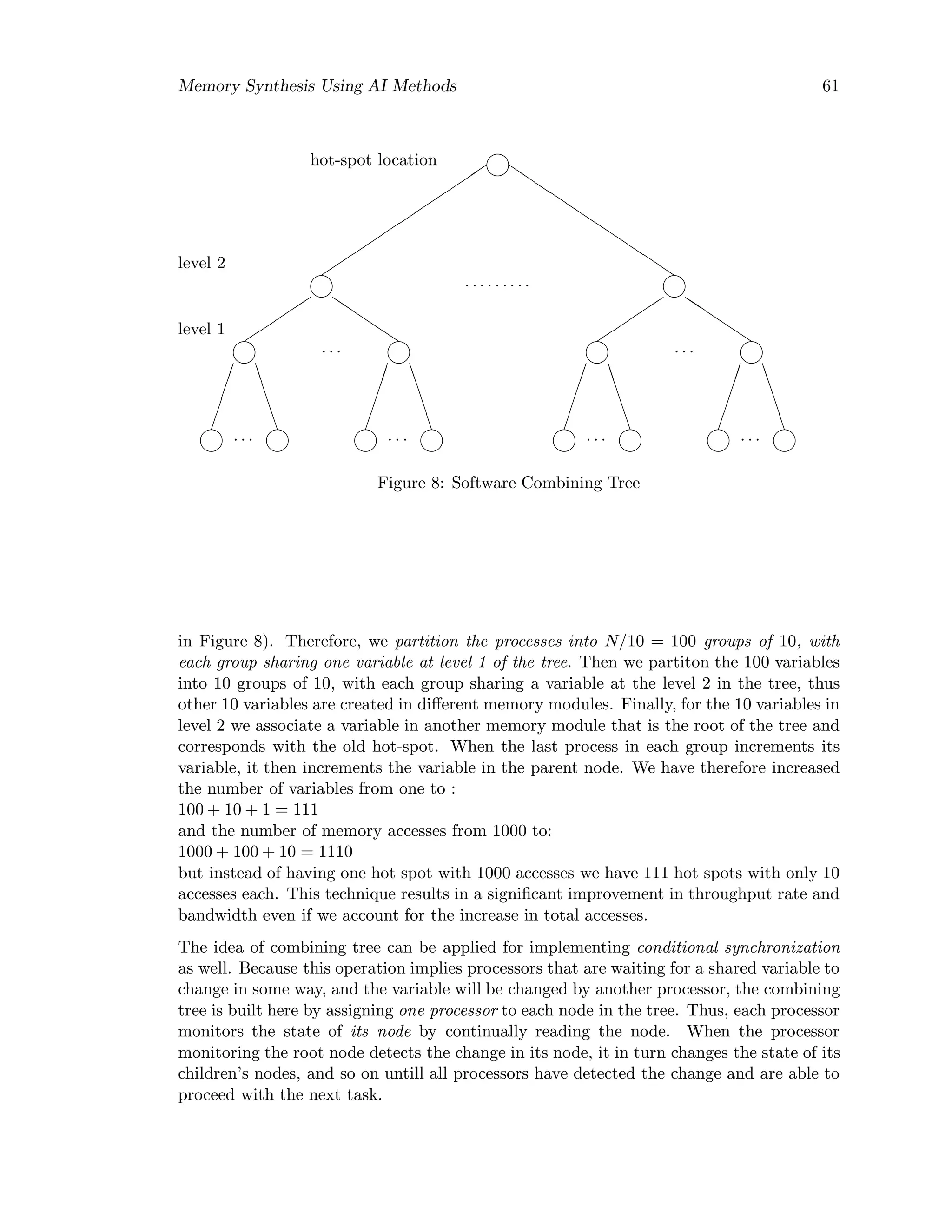
7.4.2 Software Combining Trees
A software tree can be used to eliminate memory contention due to the hot-spot variable.
The idea is similar to the concept of a combining network, but it is implemented in
software instead of hardware. A software combining tree is used to do the combining of
data accesses. This technique, that has been proposed by Yew et al. in [16], does not
require expensive hardware combining, while providing comparable performance. The
principle of a software combining tree is first illustrated for a barrier variable.
Let us assume a multiprocessor architecture with N processors and N memory modules.
We define the fan-in of the accesses to a memory location as the number of accesses to that
location. We assume a that a hot-spot with a fan-in of N exists in the system, for example
when a barrier variable (Sectuion 7.3.4) is used to make sure that all processors are finished
with a given task before proceeding. Therefore, the barrier variable is addressed by the
N processors, causing a hot-spot with a fan-in of N. The barrier variable has initially the
value zero, and each of N processors has to increment this variable so that when when all
processors are finished, the value will be N. Assuming that N = 1000, we have a hot-spot
with 1000 accesses. The software combining tree is replacing the single variable with a
tree of variables, with each variable in a different memory module. For the example given,
if we decide to reduce the fan-in to 10, then for each group of 10 processors, a variable
is created in a different memory module, for a total of 100 variables (level 1 of the tree](https://image.slidesharecdn.com/memorysynthesisusingaimethods-201006184613/75/Memory-synthesis-using_ai_methods-66-2048.jpg)
![Memory Synthesis Using AI Methods 63
8 SYSTEM CONSISTENCY MODELS
The memory consistency model is the set of allowable memory access (events) ordering.
Consistency models place requirements on the order that events from one process may be
observed by other processes in the machine. The memory consistency model defines the
logical behavior of the machine on the basis of the allowable order (sequence) of execution
within the same process and among different processes.
For the memory to be consistent, two necessary conditions must be met:
1. the memory must be kept coherent, that is, all writes to the same location are
serialized in some order and are performed in that order with respect to any
processor;
2. uniprocessor data and control dependences must be respected (this is the responsi-
bility of the hardware and the compiler) — this is required for local-level consistency.
Several memory consistency models have been proposed ([13]), such as sequential consis-
tency, processor consistency, weak consistency, and release consistency. Sequential consis-
tency is the strictest model and it requires the execution of a parallel program to appear as
some interleaving of the execution of the parallel processes on a sequential machine. This
model offers a simple conceptual programming model but limits the amount of hardware
optimization that could increase performance. The other models attempt to relax the con-
straints on the allowable event orderings, while still providing a reasonable programming
model for the programmer.
The architectural organization of a system may or may not inherently support atomicity
of memory accesses. While memory accesses are atomic in systems with a single copy of
data (a new value becomes visible to all processors at the same time), such atomicity may
not be present in cache-based systems. The lack of atomicity introduces extra complexity
in implementing consistency models. Caching of data also complicates the ordering of
accesses by introducing multiple copies of the same location. When the bus is not the
interconnection network, but general interconnection networks are used instead (non bus-
based systems), the invalidations sent by a cache may reach the other caches in the system
at different moments. Waiting for all nodes connected to the network to receive the
invalidation and to send the acknowledge would cause a serious performance penalty. As
a result of the distributed memory system and general interconnection networks being
used by scalable multiprocessor architectures (for example, the DASH architecture [9,17]
presented in Section 9.5.4), requests issued by a processor to distinct memory modules may
execute out of order. Consequently, when distributed memory and general interconnection
networks are used, performance would benefit if the consistency model allows accesses to
perform out of order, as long as local data and control dependences are observed.
The expected logical behavior of the machine must be known by the programmer in order
to write correct programs. The memory consistency has a direct effect on the complexity
of the programming model presented by a machine for the programmer.](https://image.slidesharecdn.com/memorysynthesisusingaimethods-201006184613/75/Memory-synthesis-using_ai_methods-69-2048.jpg)
![Memory Synthesis Using AI Methods 67
conservative than categorization. For example, the ordinaryL label asserts that an access
is non-competing. Since hardware may exploit the ordinaryL label to use less strict event
ordering, it is important that the ordinaryL label be used only for non-competing accesses.
However, a non-competing access can be labeled conservatively as specialL (thus, in some
cases a distinction between the categorization and the labeling of an access is made).
To ensure that accesses labeled ordinaryL are indeed non-competing, it is important that
enough competing accesses (i.e., accesses labeled as specialL) be labeled as acqL and relL.
The difficulty of ensuring enough syncL labels for a program depends on the amount of
information about the category of accesses, but it is shwon farther in this section that the
problem can be solved by following a conservative labeling strategy. Because labels at the
same level are disjoint and a label at a leaf implies all its parent labels, it follows that:
(1) an acqL or relL label implies the syncL label, and
(2) any specialL access that is not labeled as syncL is labeled as nsyncL, and
(3) any sharedL access that is not labeled as specialL is labeled as ordinaryL.
The LOAD and STORE accesses in a program are labeled based on their categorization. The
atomic read-modify-write (such as the TEST&SET primitive) provided by most architectures
is labeled by seeing it as a combination of a LOAD access and a STORE access and by labeling
separately each access based on its categorization. The common labeling for a TEST&SET
primitive is an acqL for the LOAD access and a nsyncL for the STORE access, because the
STORE access does not function as a release. If the programmer or the compiler cannot
categorize an RMW appropriately, then the conservative label for guaranteeing correctness
is: acqL for the LOAD and relL for the STORE part of the RMW.
When all accesses in a program are appropriately labeled, the program is called a properly-
labeleled (PL) program. The conditions that ensure that aprogram is properly labeled are
given in [13]:
Condition for Properly-Labeled (PL) Programs
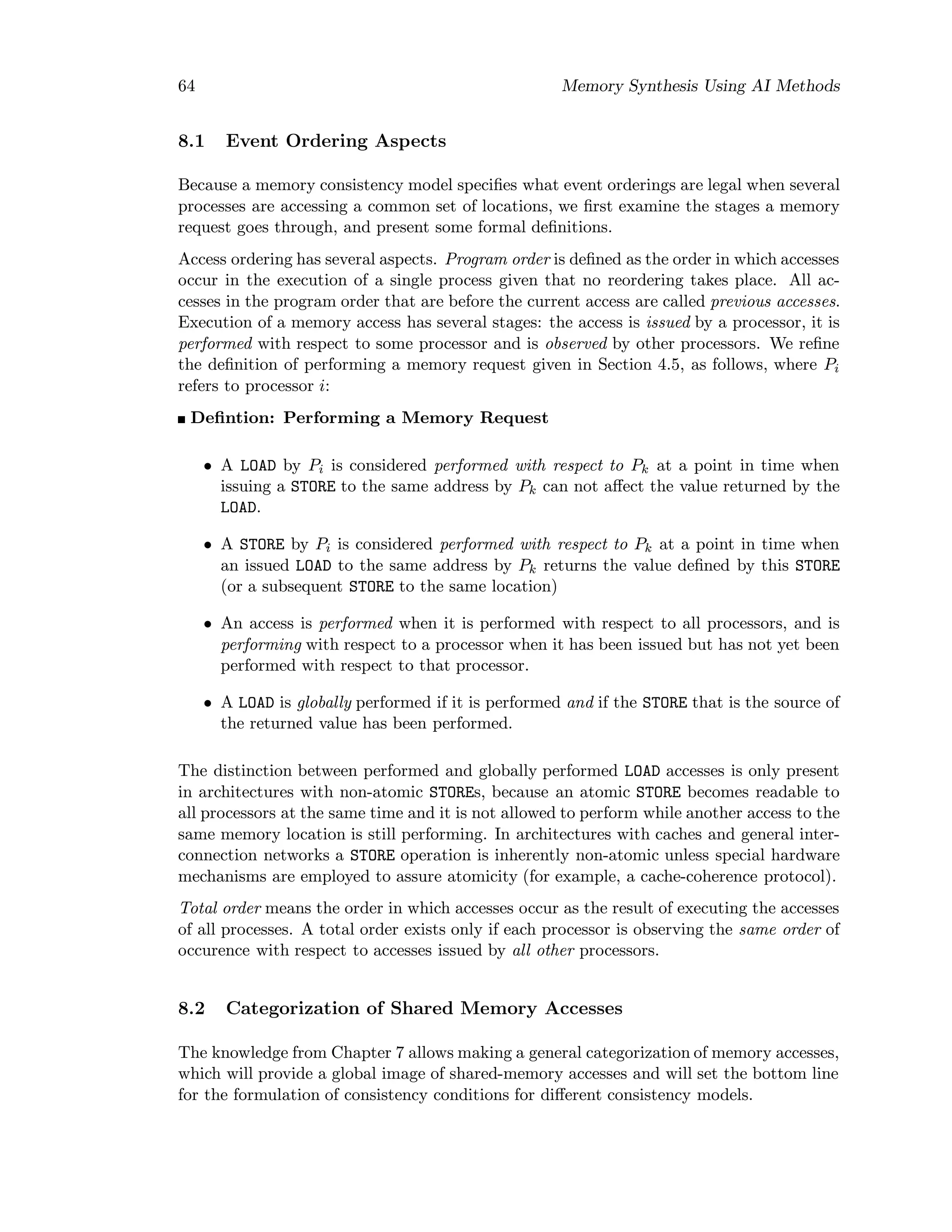
A program is properly-labeled if the following hold:
(shared access) ⊆ sharedL, competing ⊆ specialL,
and enough special accesses are labeled as acqL and relL.
There is no unique labeling to make a program a PL program, that is, there are several
labelings that respect the previous subset properties. Given perfect information about the
category of an access, the access can be easily labeled making the labels (Figure 9(b)) to
correspond to the categorization of accesses (Figure 9(a)). When perfect information to
make labeling is not available, proper labeling can still be provided by being conservative.
The three possible labeling strategies (from conservative to aggressive) are:
1. If competing and non-competing accesses can not be distinguished, then all reads
can be labeled as acqL and all writes can be labeled as relL.
2. If competing accesses can be distinguished from non-competing accesses but syn-
chronization and non-synchronization accesses can not be distinguished, then all
accesses distinguished as non-competing can be labeled as ordinaryL and all com-
peting accesses are labeled as acqL and relL (as in strategy (1)).](https://image.slidesharecdn.com/memorysynthesisusingaimethods-201006184613/75/Memory-synthesis-using_ai_methods-73-2048.jpg)
![68 Memory Synthesis Using AI Methods
3. If competing and non-competing accesses are distinguished and synchronization and
non-synchronization accesses are distinguished, then all non-competing accesses can
be labeled as ordinaryL, all non-synchronization accesses are labeled as nsyncL and
all synchronization accesses are labeled as acqL and relL (as in strategy (1)).
There are two practical ways for labeling accesses to provide properly-labeled (PL) pro-
grams. The first involves parallelizing compilers that generate parallel code from sequential
programs. Since the compiler does the parallelization, the information about which ac-
cesses are competing and which accesses are used for synchronization is known to the
compiler and can be used to label the accesses properly. The second way of producing PL
programs is to use a programming methodology that leads itself to proper labeling. For
example, a large class of programs are written such that accesses to shared data are pro-
tected within critical sections. Such programs are called synchronized programs, whereby
writes to shared locations are done in a mutually exclusive manner. In a synchronized pro-
gram, all accesses (except accesses that are part of the synchronization constructs) can be
labeled as ordinaryL. In addition, since synchronization constructs are predefined, the ac-
cesses within them can be labeled properly when the constructs are first implemented. For
this labeling to be proper, the programmer must ensure that the program is synchronized.
8.4 Sequential Consistency Model
The strictest consistency model is called Sequential Consistency (SC) and has been defined
by Lamport [2] as follows:
A system is sequentially consistent if the result of any execution
of a program is the same as if the operation of all the processors
were executed in some sequential order, and the operations of each
individual processor appear in this sequence in the order specified
by its program.
In other words, the sequential consistency model requires execution of the parallel program
to appear as some interleaving of the execution of the parallel processes on a sequential
machine. An interleaving that is consistent with the program order is called legal inter-
leaving. Application of the above definition requires a specific interpretation of the terms
operations and result. Operations are memory accesses (reads, writes, and read-modify-
writes) and result refers to the union of values returned by all the read operations in the
execution and the final state of memory. The definition of sequential consistency can be
translated in the following two conditions:
(1) all memory accesses appear to execute atomically in some total order, and
(2) all memory accesses of each processor appear to execute in an order specified by its
program, that is, in program order.
Speaking in event ordering terms, a sequential consistent memory assures that the execu-
tion of processes is such that there is a total order of memory accesses that is consistent
with the program order of each process. Under sequential consistency, identification of
accesses that form a competing pair can be achieved with the following criterion: Two](https://image.slidesharecdn.com/memorysynthesisusingaimethods-201006184613/75/Memory-synthesis-using_ai_methods-74-2048.jpg)
![Memory Synthesis Using AI Methods 69
conflicting accesses a1 and a2 on different processes form a competing pair if there exists
at least one legal interleaving where a1 and a2 are adjacent. Assuming the SC model, the
following criterion (given in [13]) may be used for determining whether enough accesses
are labeled as syncL (i.e., as acqL and relL)
Condition for enough syncL labels
Pick any two accesses u on processor Pu and v on processor Pv (Pu not the same as Pv),
such that the two accesses conflict and at least one is labeled as ordinaryL. If v appears
after (before) u under any interleaving consistent with the program order, then there needs
to be at least one relL (acqL) access on Pu and one acqL (relL) on Pv separating u and v,
such that the relL appears before the acqL. There are enough accesses labeled as syncL
—that is, relL and acqL labeled accesses— if the above condition holds for all possible
pairs u and v.
The SC model ignores all access labelings past sharedL. In systems that are sequentially
consistent we say that events are strongly ordered: the order in which events are generated
by a processor is the same as the order in which all the other processors observe the
events, and events generated by two different processors are observed in the same order
by all other processors.
8.4.1 Conditions for Sequential Consistency
Necessary and Sufficient Conditions for SC in Systems with Atomic Accesses
It has been shown by Dubois et al. ([3]) that the necessary and suficient condition for a
system with atomic memory accesses to be sequentially consistent is that memory accesses
be performed in program order.
In architectures with caches and general interconnection networks, where accesses are
inherently non-atomic, special hardware and software mechanisms must be employed to
assure sequential consistency. Here are the suficient conditions for sequential consistency
(as given in [13]) in systems with non-atomic accesses:
Sufficient Conditions for SC in Systems with Non-Atomic Accesses
(1) before a LOAD is allowed to perform with respect to any other processor, all previous
LOAD accesses must be globally performed and all previous STORE accesses must be per-
formed, and
(2) before a STORE is allowed to perform with respect to any other processor, all previ-
ous LOAD accesses must be globally performed and all previous STORE accesses must be
performed.
8.4.2 Consistency and Shared-Memory Architecture
Let us examine the consistency model for the common shared-memory architectures:
shared-bus systems without caches, shared-bus systems with caches, systems with gen-
eral interconnection networks without caches, and systems with general interconnection
networks with caches.](https://image.slidesharecdn.com/memorysynthesisusingaimethods-201006184613/75/Memory-synthesis-using_ai_methods-75-2048.jpg)
![Memory Synthesis Using AI Methods 71
only be consistent at those points.
Several memory consistency models that attempt to relax the constraints on the allowable
event orderings have been proposed and they are called relaxed consistency models. The
most prominent relaxed consistency models are the processor consistency, weak consis-
tency, and release consistency models. The larger latencies found in a distributed system,
as compared to a shared-bus system, favor the relaxed consistency models because they
allow more performant implementations than those allowed by the sequential consistency
model.
8.5 Processor Consistency Model
The processor consistency (PC) model requires that all writes issued from a processor may
be only observed in the order in which they were issued, but allows that the order in which
writes from two processors occur, as observed by themselves or a third processor, may not
be identical. The conditions for processor consistency are defined in [13] as follows:
Conditions for Processor Consistency
(1) before a LOAD is allowed to perform with respect to any other processor, all previous
LOAD accesses must be performed, and
(2) before a STORE is allowed to perform with respect to any other processor, all previous
accesses (LOADs and STOREs) must be performed.
The above conditions allow reads following a write to bypass the write. To avoid deadlock,
the implementation should guarantee that a write that appears previously in program order
will eventually perform. The PC model ignores all access labelings aside from sharedL.
8.6 Weak Consistency Model
The weak consistency model and the release consistency model (next Section) employ the
categorization and labeling of memory accesses (Section 8.2 and 8.3) to relax the event
ordering restrictions on the basis of extra information (provided by the programmer or
the compiler) on the type of memory access.
The weak consistency model proposed by Dubois et al. ([3]) is based on the idea that the
interaction between parallel processes manifests itself through synchronization accesses
that are used to order events and through ordinary shared accesses. If synchronization ac-
cesses can be recognized, and sequential consistency is guaranteed only for synchronization
accesses, then the ordinary accesses might proceed faster because they need to be ordered
only with respect to synchronization accesses. This improves performance because ordi-
nary accesses are more frequent than synchronization accesses. As an example, consider a
processor updating a data structure within a critical section. If updating the structure re-
quires several writes, each write in a sequentially consistent system will stall the processor
untill all other cached copies of that location have been invalidated. But these stalls are
unnecessary, as the programmer has already made sure that no other process can rely on
the consistency of that data structure until the critical section is exited. If the synchro-](https://image.slidesharecdn.com/memorysynthesisusingaimethods-201006184613/75/Memory-synthesis-using_ai_methods-77-2048.jpg)
![72 Memory Synthesis Using AI Methods
nization points can be identified, then the memory need need only be consistent at those
points. The weak consistency model exploits this idea and guarantees that the memory
is consistent only following a synchronization operation. The conditions that ensure weak
consistency are given in [13]:
Conditions for Weak Consistency
(1) before an ordinary LOAD or STORE access is allowed to perform with respect to any
other processor, all previous synchronization accesses must be performed,
(2) before a synchronization access is allowed to perform with respect to any other pro-
cessor, all previous ordinary (LOADs and STOREs) accesses must be performed, and
(3) synchronization accesses are sequentially consistent with respect to one another.
Speaking in terms of access labeling, under the weak consistency model only the la-
bels sharedL, ordinaryL, and specialL are taken into account, with an access labeled as
specialL being treated as a synchronization access and as both an acquire and a release.
In a machine supporting weak consistency (also called weak ordering of events [3,13,17]) the
programmer should make no assumption about the order in which the events that a process
generates are observed by other processes between two explicit synchronization points.
Accesses to shared writable data should be executed in a mutually exclusive manner,
controlled by synchronization operations, such as LOCK and UNLOCK. Only synchronization
accesses are guaranteed to be sequentially consistent. Before a synchronization access
can proceed, all previous ordinary accesses must be allowed to “settle down” (i.e., all
shared memory accesses made before the synchronization point was encountered must be
completed before the synchronization access can proceed). In such systems we say that
events are weakly ordered.
The advantage of the weak consistency model is that it provides the user with a reasonable
programming model, while permitting multiple memory accesses to be pipelined, and thus
allowing high-performance. For example, consider a multiprocessor with a buffered, mul-
tistage, and packet-switched interconnection network. If strong ordering is to be enforced,
then the interface between the processor and the network can send global memory requests
only one at a time. The reason for this is that in such a network the access time is vari-
able and unpredictible because of conflicts; in many cases waiting for an acknowledgement
from the memory controller is the only way to ensure that global accesses are performed
in program order. In the case of weak ordering the interface can send the next global
access directly after the current global access has been latched ih the first stage of the
interconnection network, resulting in better processor efficiency. However, the frequency
of synchronization operations (such as LOCKs) will be higher in a program designed for a
weakly ordered system. Therefore, weak consistency is expected to be more performant
than sequential consistency in systems that do not synchronize frequently.
The disadvantage of the weak consistency model is that the programmer or the com-
piler must identify all synchronization accesses in order to support mutually exclusive
access to shared writable data. Moreover, the synchronization accesses must be hardware-
recognizable to enforce that they are sequentially consistent.](https://image.slidesharecdn.com/memorysynthesisusingaimethods-201006184613/75/Memory-synthesis-using_ai_methods-78-2048.jpg)
![Memory Synthesis Using AI Methods 73
8.7 Release Consistency
The release consistency model (RC) is an extension of the weak consistency model, in
which the requirements on synchronization accesses and ordinary accesses ordering are
relaxed. The release consistency model exploits the information conveyed by the labels at
the leaves of the labeling tree, that is, the labelings ordinaryL, nsyncL, acqL, and relL
are considered by the model. Basically, RC guarantees that memory is consistent only
when a critical section is exited. The conditions for ensuring release consistency are given
in [13] as follows:
Conditions for Release Consistency
(1) before an ordinary LOAD or STORE access is allowed to perform with respect to any
other processor, all previous acquire accesses must be performed,
(2) before a release access is allowed to perform with respect to any other processor, all
previous ordinary (LOADs and STOREs) accesses must be performed, and
(3) special accesses are processor consistent with respect to one another.
The ordering condition stated by the weak consistency model for synchronization accesses
is extended under the release consistency model to special accesses, that include all compet-
ing accesses, both synchronization and non-synchronization accesses. On the other hand,
four of the ordering restrictions in weak consistency are not present in release consistency:
1. First, ordinary LOAD and STORE accesses following a release access do not have to wait
for the release access to be performed. Because the release synchronization access
is intended to signal that previous LOAD and STORE accesses in a critical section are
complete, it is not related to the ordering of the future accesses. Of course, the local
dependences within a processor must still be respected by LOADs and STOREs.
2. Second, an acquire synchronization access need not be delayed for previous ordinary
LOAD and STORE accesses to be performed. Because an acquire access is intended
to prevent future accesses by other processors to a set of shared locations, and is
not giving permission to any other process to access the previous pending locations,
there is no reason for the acquire to wait for the pending accesses to complete.
3. Third, a non-syncronization special access does not wait for previous ordinary ac-
cesses and does not delay future ordinary accesses; therefore, a non-synchronization
access does not interact with ordinary accesses.
4. Fourth, the special accesses are only required to be processor consistent and not
sequentially consistent. The reason for this is that, provided that the applications
meet some restrictions, sequential consistency and processor consistency for special
accesses give the same results. The restrictions that allow this relaxed requirement
on special accesses are given in [13] and have been verified there to hold for the
parallel applications available at the time the study has been conducted.
Essentially, RC guarantees that the memory is consistent when a critical section is exited,
by requiring that all ordinary memory operations be performed before the critical section](https://image.slidesharecdn.com/memorysynthesisusingaimethods-201006184613/75/Memory-synthesis-using_ai_methods-79-2048.jpg)
![Memory Synthesis Using AI Methods 79
coherence protocols —write invalidate and write update— exhibit performance dependent
on the sharing pattern. Snooping protocols may use either write invalidate or write update,
while directory-based protocols use write invalidate. Write-invalidate schemes maintain
cache coherence by invalidating copies of a memory block when the block is modified by a
processor. For snooping-based protocols, the invalidation is broadcast and all caches are
checking if they have a copy of the line that must be invalidated, while for directory-based
protocols only the caches that actually share the line receive the invalidation message.
The sharing pattern is characterized by several parameters, of particular importance be-
ing the number of caches sharing a data object and the write-run. The write-run has
been defined by Eggers and Katz [18] as the length of the uninterrupted sequence of write
requests interspread with reads to a shared cache line by one processor. A write-run is
terminated when another processor reads or writes the same cache line. The length of
the write-run is the number of writes in that write-run. Every new write-run requires an
invalidation and data transfer. When write-runs are short, the write-invalidate scheme
generates frequent invalidations and the write update scheme generates equally frequent
updates. Since the total time cost for invalidations and data transfer is higher than the
cost of updating one word, write-invalidate schemes are inferior for this sharing pattern.
On the other hand, for long write-runs, the write update scheme generates many updates
that are redundant, given the length of the write-run. Therefore, write invalidate performs
better for long write-runs because only the first write in a write-run causes invalidation
of the shared copies of the written line. Furthermore, a write invalidate scheme in a
directory-based protocol sends one invalidation request per write-run only to the caches
that actually share the line. A study conducted on a simulated 32-processor machine [9]
shows that, for a large number of applications, most writes cause invalidations to only a
few caches, with only about 2% of all shared writes causing invalidation of more than 3
caches. Write invalidate protocols perform fairly well for a broad range of sharing pat-
terns. However, there exist some sharing patterns for which unnecessary invalidations are
generated. A notable example is the invalidation overhead associated with data structures
that are accessed within critical sections. Typically, processors read and modify such data
structures one at a time. Processors that access data this way cause a cache miss followed
by an invalidation request being sent to the cache attached to the processor that most
recently exited the critical section. This sharing behavior, denoted migratory sharing has
been previously shown to be the major source of single invalidations (i.e., invalidation of
one cache) by Gupta and Weber in [14]. An extension of the write-invalidate protocol
that effectively eliminates most single invalidations caused by migratory sharing has been
proposed by Stenstr¨om et al. in [19]. This scheme improves performance by reducing the
shared access penalty and the network traffic.
9.4 Snooping Protocols
9.4.1 Implementation Issues
A bus is a convenient device for ensuring cache coherence because it allows all processors
in the system to observe ongoing memory transactions. In a snooping protocol each cache
snoops on the transactions of other caches. When the cache controller sees an invalidation](https://image.slidesharecdn.com/memorysynthesisusingaimethods-201006184613/75/Memory-synthesis-using_ai_methods-85-2048.jpg)
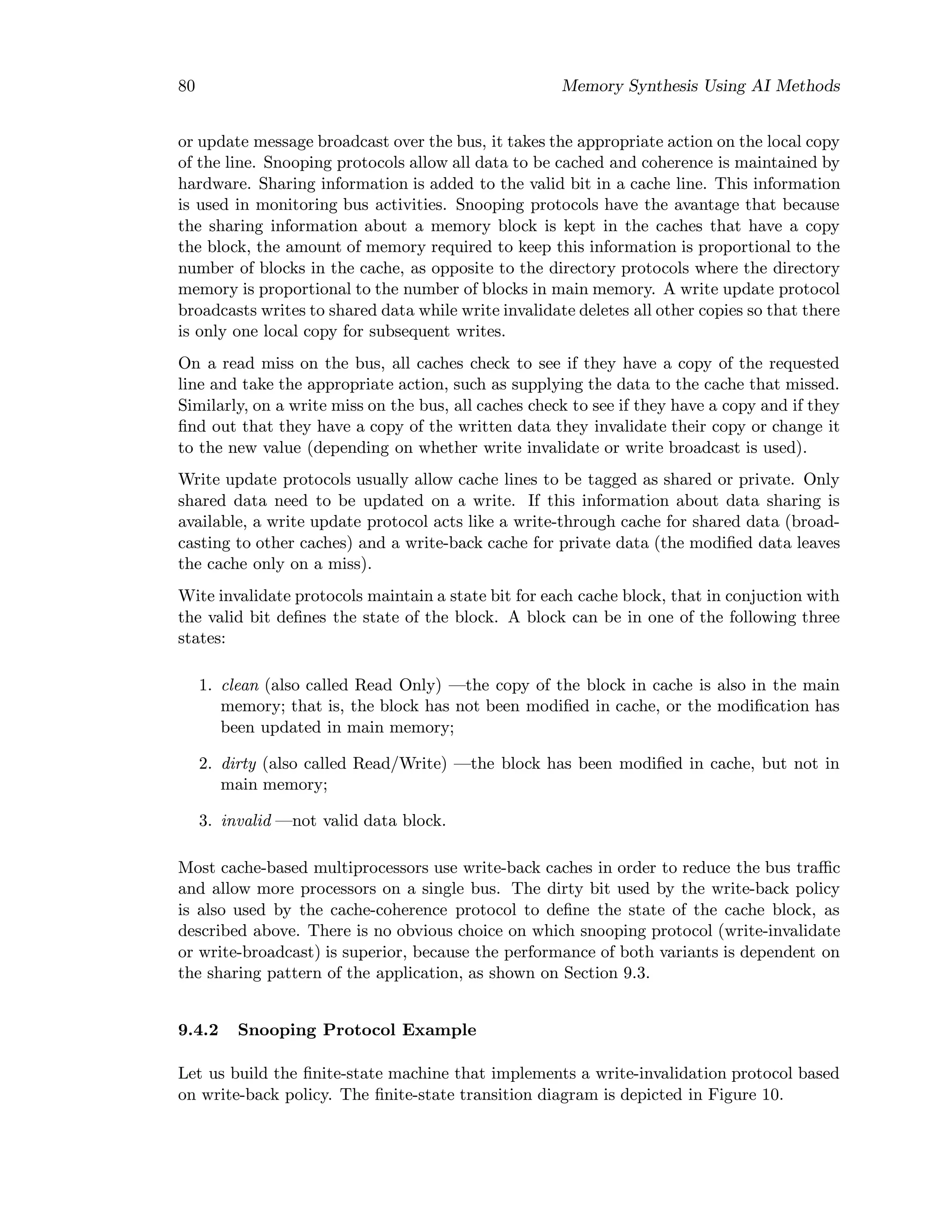
![82 Memory Synthesis Using AI Methods
There is only one state-machine in a cache, with stimuli coming either from the attached
CPU or from the bus, but the figure shows the three states of the protocol in duplicate
in order to distinguish the transitions based on CPU actions, as opposed to transitions
based on bus operations. Transitions happen on read misses, write misses, or write hits;
read hits do not change cache state.
When the CPU has a read miss, it will change the state of that block to Read only and
write back the old block if it was in the Read/Write state (dirty). All the caches snoop
on the read miss to see if this block is in their cache. If one cache has a copy and it is
in the Read/Write state, then the block is written to memory and is then changed to the
Invalid state (as shown in this protocol) or Read only.
When a CPU writes into a block, that block goes to the Read/Write state. If the write
was a hit, an invalidate signal goes out over the bus. Because caches monitor the bus, all
check to see if they have a copy of that block; if they do, they invalidate it. If the write
was a miss, all caches with copies go to the invalid state. For simplicity, write to clean
data may be treated as a “write miss”, so that there is no separate signal for invalidation,
but the same bus signal as for write miss is used.
9.4.3 Improving Performance of Snooping Protocol
Reducing Interference Between Broadcasts and CPU Operation
Since every bus transaction checks cache-address tags, it would interfere with the CPU
accesses to cache if only a copy of the address tag were accessed both by CPU and snooping.
To remove this problem, the address tag portion of the cache is duplicated so that an extra
read port is available for snooping; these two identical copies of the address tag are called
snoop tag and normal tag respectively. In this way, snooping interferes with the CPU’s
accesses to the cache only when the tags must be changed, that is, when the CPU has a
miss or when a coherence operation occurs. On a miss, the CPU arbitrates with the bus
to change the snoop tags as well as the normal tags (to keep the address tags coherent).
When a coherence operation occurs in the cache, the CPU will likely stall, since the cache
is unavailable.
Reducing Invalidation Interference
Some designs ([20]) are queuing the invalidation requests. A list of the addresses to be
invalidated is maintained in a small hardware-implemented queue called Buffer Invalida-
tion Address Stack (BIAS). The BIAS has a high priority for cache cycles, and if the
target line is found in the cache, it is invalidated. To reduce the interference between the
invalidation accesses to cache and the normal CPU accesses, a BIAS filter memory ([20])
may be used. A BFM is associated with each cache and works by filtering out repeated
requests to invalidate the same block in a cache.
Snooping protocols are fairly simple and not expensive. For multiprocessors with a small
number of processors they perform well. The disadvantage is that the snooping protocols
are not scalable. Buses don’t have the bandwidth to support a large number of processors.
The coherence traffic quickly increases with the number of processors because snooping
protocols require that all caches see every memory request from every processor. The](https://image.slidesharecdn.com/memorysynthesisusingaimethods-201006184613/75/Memory-synthesis-using_ai_methods-88-2048.jpg)
![Memory Synthesis Using AI Methods 83
shared bus and the need to broadcast every memory request to all processor caches inher-
ently limit the scalability of snooping protocol-based machines, because the common bus
and the individual processor caches eventually saturate.
9.5 Directory-based Cache Coherence
9.5.1 Classification of Directory Schemes
A directory is a list of the locations of the cached copies for each line of shared data. A
directory entry is associated with each memory block and contains a number of pointers
to specify the locations of copies of the block and a state bit to specify whether ot not a
unique cache has permission to write that line.
Depending on the amount of information stored in a directory entry, directory protocols
fall in two categories:
• full-map directories —the directory stores for each block in global memory informa-
tion about all caches in the system, so that every cache can simultaneously have a
copy of any block of data. In this case, the pointers in a directory entry are simply
presence bits associated with each cache. This type of protocol has the advantage
of allowing full-sharing of any memory block, but is not scalable with respect to
memory overhead. Indeed, assuming that the amount of shared memory increases
linearly with the number of processors, N, then, because the size of a directory entry
is proportional to the number of processors, and the number of entries is equal to
the number of blocks that is proportionat to the memory size, it results that the size
of directory is Θ(N) ∗ Θ(N) = Θ(N2).
• limited directories —each directory entry has a fixed number of pointers, regardless
of the number of caches in the system; they have the disadvantage of restricting the
number of simultaneously cached copies of a memory block, but have the advan-
tage of limiting the growth of the directory to a constant factor of the number of
processors.
When only an unique directory is accessed by all the caches in the system, the directory
structure is called centralized directory. The architecture of a system using a full-map
centralized-directory coherence protocol is shown in Figure 11. The main memory (and
the directory) can be made up from several memory modules.
9.5.2 Full-Map Centralized-Directory Protocol
The classical centralized-directory protocol is a full-map protocol and has been first pro-
posed by Censier and Feautrier [1]. For each block of shared-memory there is a directory
entry that contains:
• one presence bit per processor cache. The set of presence bits is a bit vector called
the presence vector;](https://image.slidesharecdn.com/memorysynthesisusingaimethods-201006184613/75/Memory-synthesis-using_ai_methods-89-2048.jpg)
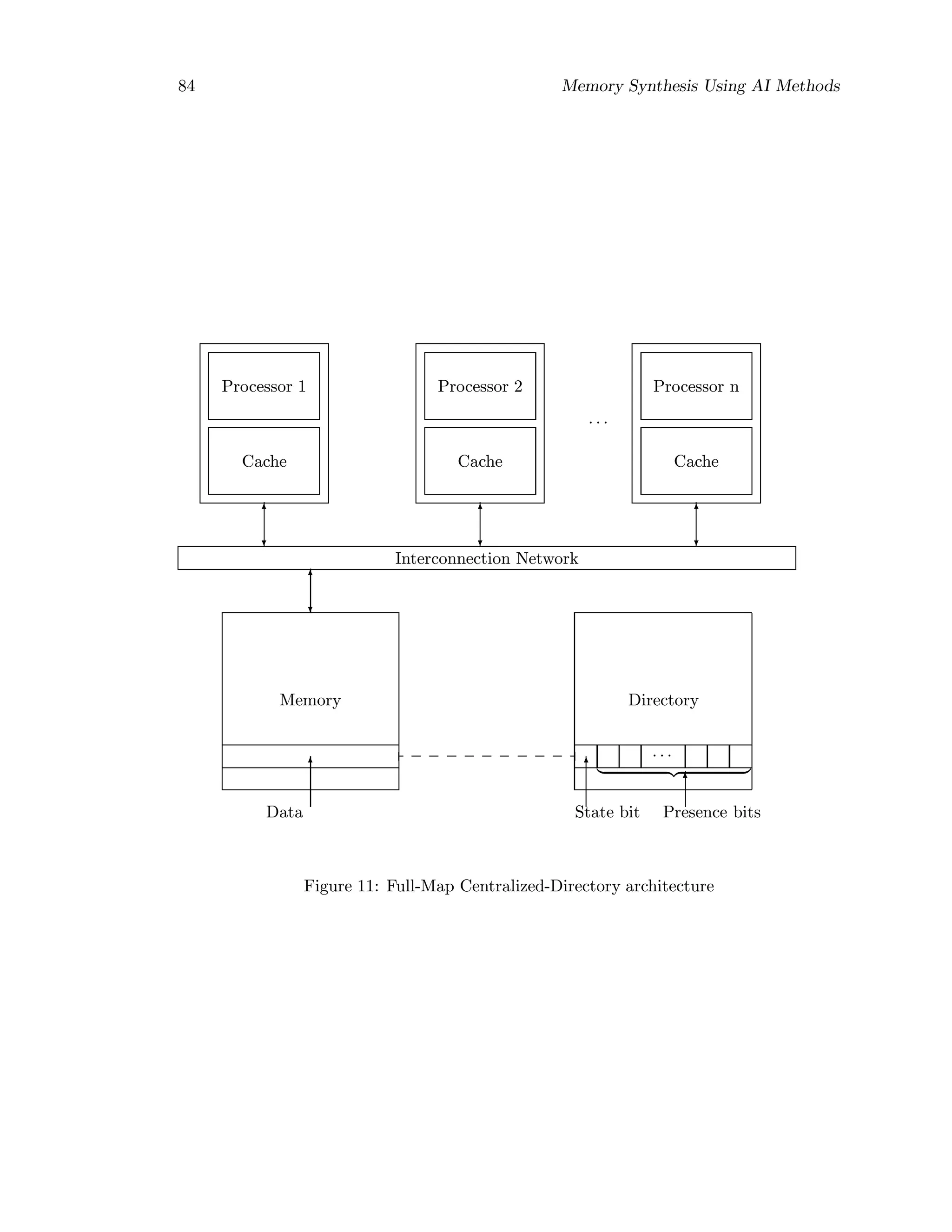
![86 Memory Synthesis Using AI Methods
5. The main meory receives the acknowledgement, sets the dirty bit, clears the presence
bit for cache C1, and sends write permission to cache C2;
6. Cache C2 receives the write permission message, updates line X, sets the private
bit, and reactivates processor P2.
If processor P2 issues another write to a word in line X and cache C2 still owns line X,
then the write takes places immediately into the cache.
If processor P1 attempts to read a word in line X, after P2 has got ownership of line X,
then the following events will occur:
1. Cache C1 detects that the line X containing the word is in invalid state;
2. Cache C1 issues a read request to the main memory and stalls processor P1;
3. The main memory checks the dirty and presence bits in the directory entry for line
X and finds out that line X is dirty and cache C2 has the only valid copy of line X.
4. The main memory issues a read request for line X to cache C2;
5. Cache C2 receives the read request for line X from main memory, clears the private
bit, and sends the line to the main memory;
6. The main memory receives the line X from cache C2, clears the dirty bit, sends line
X to cache C1, and sets the presence bit for C1;
7. Cache C1 fetches the line X, sets the valid bit, and reactivates processor P1.
The disadvantage of this directory scheme is that it is not scalable with respect to the
directory overhead because directory size is Θ(N2
), where N is the number of processors,
that is, the memory overhead scales as the square of the number of processors.
9.5.3 Limited-Directory Protocol
The limited directory protocol, as proposed by Agarwal et al. [10] is designed to solve the
directory size problem, by allowing a constant number of caches to share any block, so
that the directory entry size does not change as the number of processors in the system
increases. A directory entry in a limited-directory protocol contains a fixed number of
pointers —denoted by i— which indicate the caches holding a copy of the line, and a
dirty bit (with the same meaning as for the full-map directory) for the line. The limited-
directory protocol is similar to the full-map directory, except in case when more than i
caches request read copies of a particular line of data.
An i-pointer directory may be viewed as an i-way set-associative cache of pointers to
shared copies. When the i+1 -th cache requests a copy of line X, the main memory must
invalidate one copy in one of the i caches currently sharing the line X, and replace its
pointer with the pointer to the cache that will share the line. This process of pointer](https://image.slidesharecdn.com/memorysynthesisusingaimethods-201006184613/75/Memory-synthesis-using_ai_methods-92-2048.jpg)
![Memory Synthesis Using AI Methods 87
replacement is called eviction. Since the directory acts as a set-associative cache, it must
have a pointer replacement strategy. Pseudorandom eviction requires no extra memory
overhead and is a good choice for replacement policy. A pointer in the directory entry
encodes binary processor (and cache) identifiers, so that for a system with N processors
a pointer requires log2N bits of memory. Therefore a directory entry requires i ∗ log2N
bits and under the assumption that the amount of memory (and hence the number of
memory lines) increases linearly with the number of processors it follows that the memory
overhead of the limited-directory protocol is:
Θ(i ∗ log2N) ∗ Θ(N) = Θ(N ∗ log2N)
Because the memory overhead grows approximately linearly with the number of proces-
sors, this protocol is scalable with respect to memory overhead. This protocol works well
for data that are not massively shared, but for highly shared data, as a barrier synchroniza-
tion variable, pointer thrashing occurs because many processors spin-lock on the barrier
variable.
Both limited-directory and full-map directory protocols present the drawback of using
a centralized directory which may become a bottleneck when the number of processors
increases. If the memory and directory are partitioned into independent units and con-
nected to the processors by scalable interconnect, the memory system can provide scalable
memory bandwidth — this is the idea of distributed directory and memory, presented in
the next Subsection.
9.5.4 Distributed Directory and Memory
The idea is to achieve scalability by partitioning and distributing both the directory and
main memory, using a scalable interconnection network and a coherence protocol that
can suitably exploit distributed directories. The architecture of such a system is shown
in Figure 12, that depicts the Stanford DASH Multiprocessor [9] architecture. The name
DASH is an abbreviation for Directory Architecture for Shared Memory. The architecture
provides both the ease of programming of single-address-space machines (with caching
to reduce memory latency) and the scalability that was previously achievable only with
message-passing machines but not with cache-coherent shared-address machines.
The DASH architecture consists of a set of clusters (also called processing nodes) connected
by a general interconnection network. Each cluster consists of a small number (e.g., eight)
of high-performance processors and a portion of the shared memory interconnected by a
bus. Multiprocessing within the cluster may be viewed either as increasing the power of
each processing node or as reducing the cost of the directory and network interface by
amortizing it over a larger number of processors. The Dash architecture removes the scal-
ability limitation of centralized-directory architectures by partitioning and distributing
the directory and main memory, and by using a new coherence protocol that can suitably
exploit distributed directories. Distributing memory with the processors is essential be-
cause it allows the system to exploit locality. All private data and code references, along
with some of the shared references, can be made locally to the cluster. These references
avoid the longer latency of remote references and reduce the bandwidth demands on the
global interconnection.](https://image.slidesharecdn.com/memorysynthesisusingaimethods-201006184613/75/Memory-synthesis-using_ai_methods-93-2048.jpg)
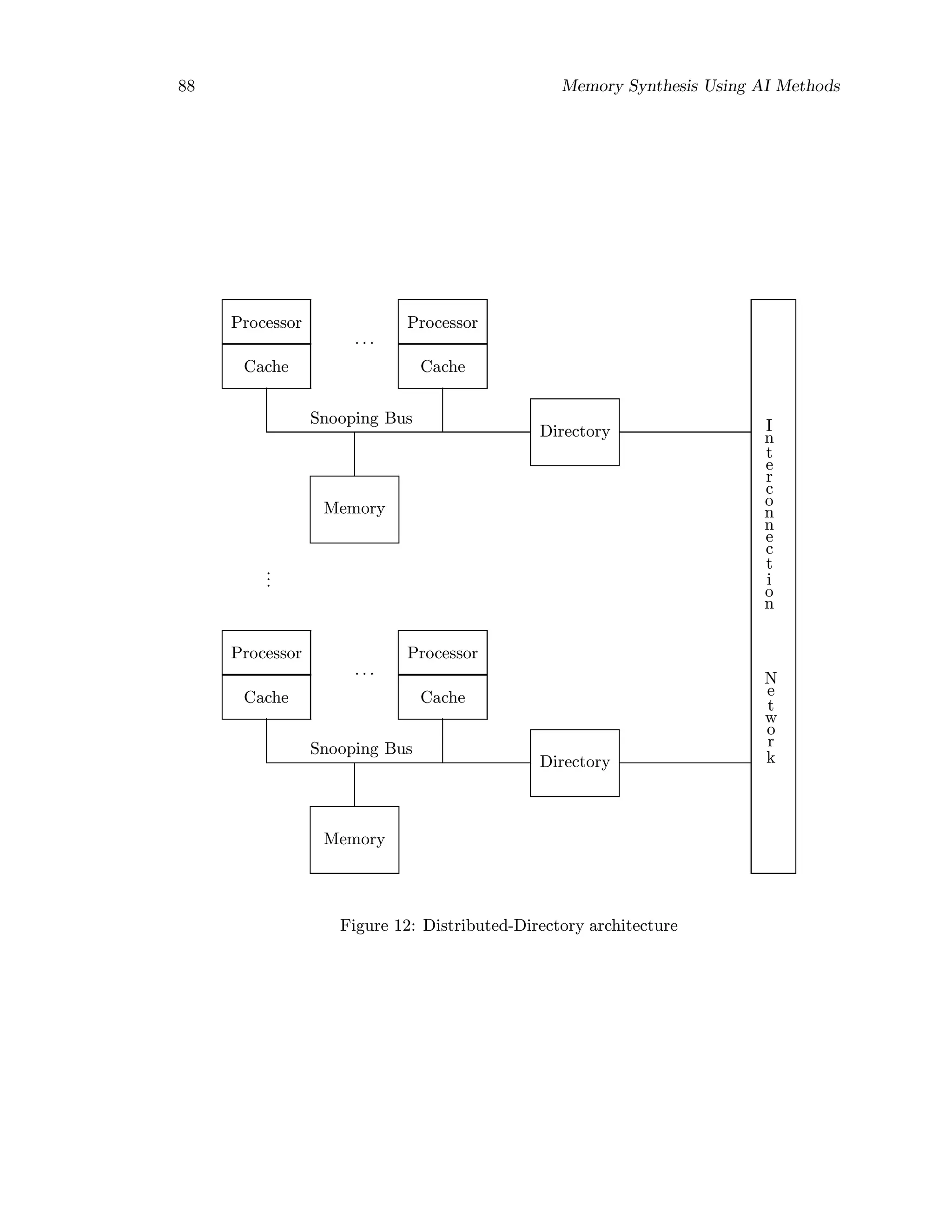
![90 Memory Synthesis Using AI Methods
medium N, this growth is tolerable. For examle, consider a machine in which a cluster
contains 8 processors and has a cache line-size of 32 bytes. For N = 32, that is, 256
processors, the overhead for directory memory is only 12.5 percent of physical memory,
which is comparable with the overhead of supporting an error-correcting code on memory.
For larger machines, where the overhead would become intolerable with a the full-map
directory, one can use the following approach to achieve scalability: the full-map directory
is replaced with a limited directory that has a small number of pointers (Subsection 9.5.3)
and, in the unusual case when the number of pointers is smaller the the number of clusters
caching a line, invalidations are broadcast on the interconnection network. The reason that
limited directory can be used is based on the data sharing and write-invalidate patterns
exhibited by most applications. For example, it is shown in [9] that most writes cause
invalidations to only a few caches, with only about 2% of shared writes causing invalidation
of more than 3 caches.
To the memory present within each cluster a directory memory is associated. Each di-
rectory memory is contained in a Directory Controller (DC). The DC is responsible for
maintaining the cache coherence across the clusters and serving as interface to the in-
terconnection network. The clusters and their associated portion of main memory are
categorized in three types, according to the role played in a given transaction:
1. the local cluster — is the cluster that contains the processor originating a given
request; local memory refers to the main memory associated with the local cluster.
2. the home cluster — is the cluster that contains the main memory and directory for
a given physical memory address.
3. a remote cluster — is any other cluster; remote memory is any memory whose home
is not the local.
Therefore, the Dash memory system can be logically broken into four levels of hierarchy,
as shown in Figure 13.
States in Directory and in Caches
The directory memory is organized as an array of directory entries. There is one entry for
each memory block of the corresponding memory module. A directory entry contains the
following pieces of information:
1. a state bit that indicates whether the clusters have a read (shared) or read/write
(dirty) copy of the data.
2. a presence bit-vector, which contains a bit for each of the clusters in the system.
If the state bit indicates a read copy and none of the presence bits is set to one, then the
block is said to be uncached. A memory block can be in one of three states, as indicated
by the associated directory entry:
1. uncached-remote, that is, not cached by any remote cluster;](https://image.slidesharecdn.com/memorysynthesisusingaimethods-201006184613/75/Memory-synthesis-using_ai_methods-96-2048.jpg)
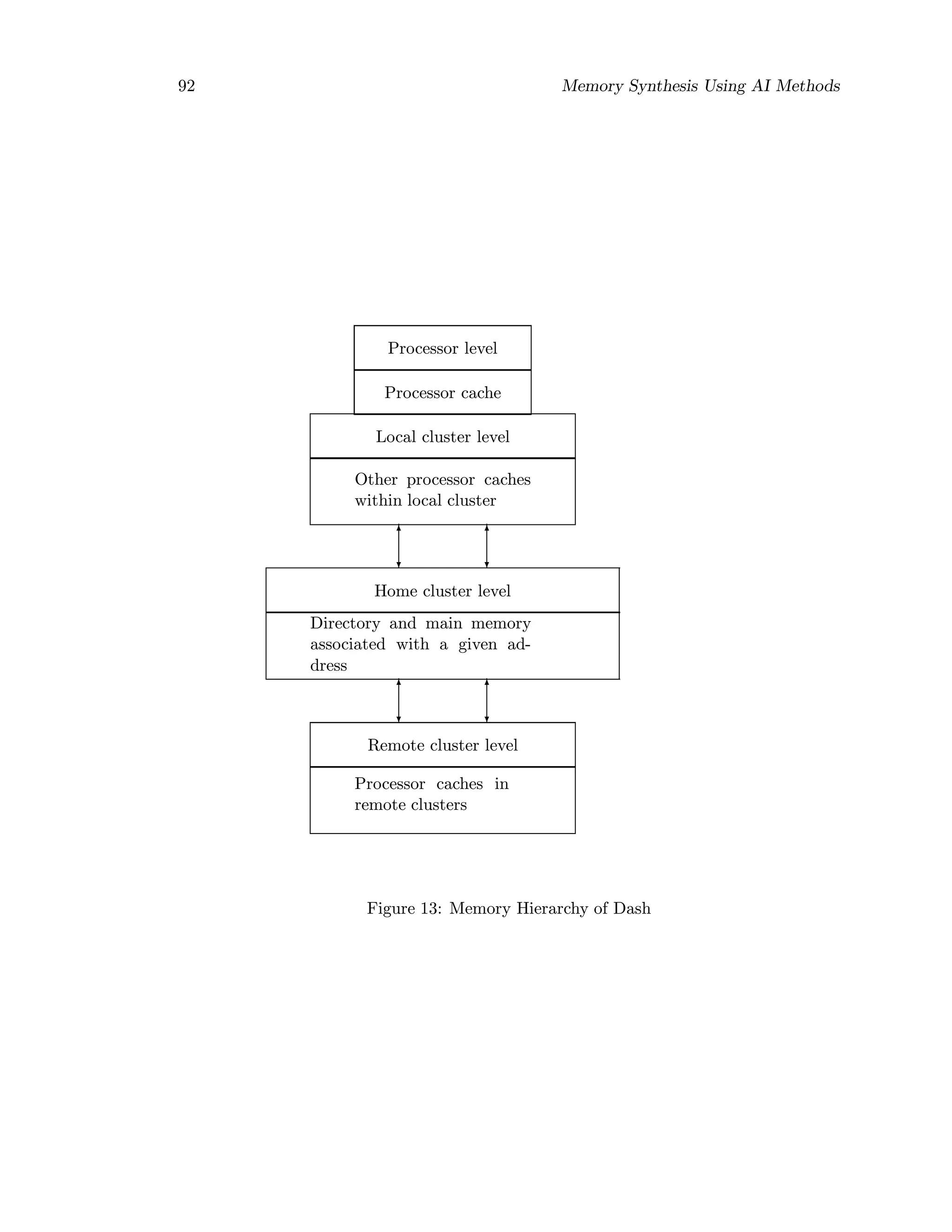
![94 Memory Synthesis Using AI Methods
9.6 Compiler-directed Cache Coherence Protocols
Software-based coherence protocols require compiler assistance. Compile-time analysis is
used to obtain information on accesses to a given line by multiple processors. Such infor-
mation can allow each processor to manage its own cache without interprocessor runtime
communication. Compiler-directed management of of caches implies that a processor has
to issue explicit instructions to invalidate cache lines.
To eliminate the stale-date problem caused by process migration the following method can
be used:
Cache-flushing
To eliminate the stale-data problem for cacheable, nonshared data, the processor can flush
its cache each time a program leaves a processor. This guarantees that main memory
becomes the current active location for each variable formerly held in cache. The cache
flush approcah can also be used for the I/O cache-coherence problem (Section 5.13.1).
While this solution prevents the stale-data from being used, the cache invalidations caused
by flushes may have as effect an increase in Miss Rate.
Regarding the coherence problem caused by accesses to shared data, there are two simple
coherence schemes:
Not caching shared data
Each shared datum can be made noncacheable to eliminate the difficulty in finding its
current location among caches and main memory. Data can be done noncacheable by
several methods, for example, by providing a special range of addresses for noncacheable
data, or by using special LOAD and STORE instructions that do not access cache at all.
Not caching shared writable data
This is an improvement of the previous method. Since for performance consideration it is
desirable to attach a private cache to each CPU, one can prevent data inconsistency by
not caching shared writable data, that is, by making such data noncacheable. Examples
of shared writable data are locks, shared data structures such as process queues, and any
other data protected by critical sections. When shared writable data are not cached, no
coherence problem can occur. This solution is implemented using programmer’s directives
that instruct the compiler to allocate shared writable data to noncacheable regions of
memory. The drawback of this scheme is that large data structures cannot be cached,
although most of the time it would be safe to do so.
While these solutions have the advantage of simple implementation, they have a negative
effect on performance because they reduce the effective use of cache. As pointed out in
many works (for example, in [8]), shared-data accesses acount for a large portion of global
memory accesses. Therefore, allowing shared writable data to be cached when it is safe to
do so is crucial for performance.
Efficient Compiler-directed Cache Coherence
We shall present an efficient compiler-directed scheme following the ideas from Cheong
and Veidenbaum [8]. Basically, caching is allowed when it is safe, and cache flush is made
when coherence problems occur. The operating environment of the coherence algorithm](https://image.slidesharecdn.com/memorysynthesisusingaimethods-201006184613/75/Memory-synthesis-using_ai_methods-100-2048.jpg)
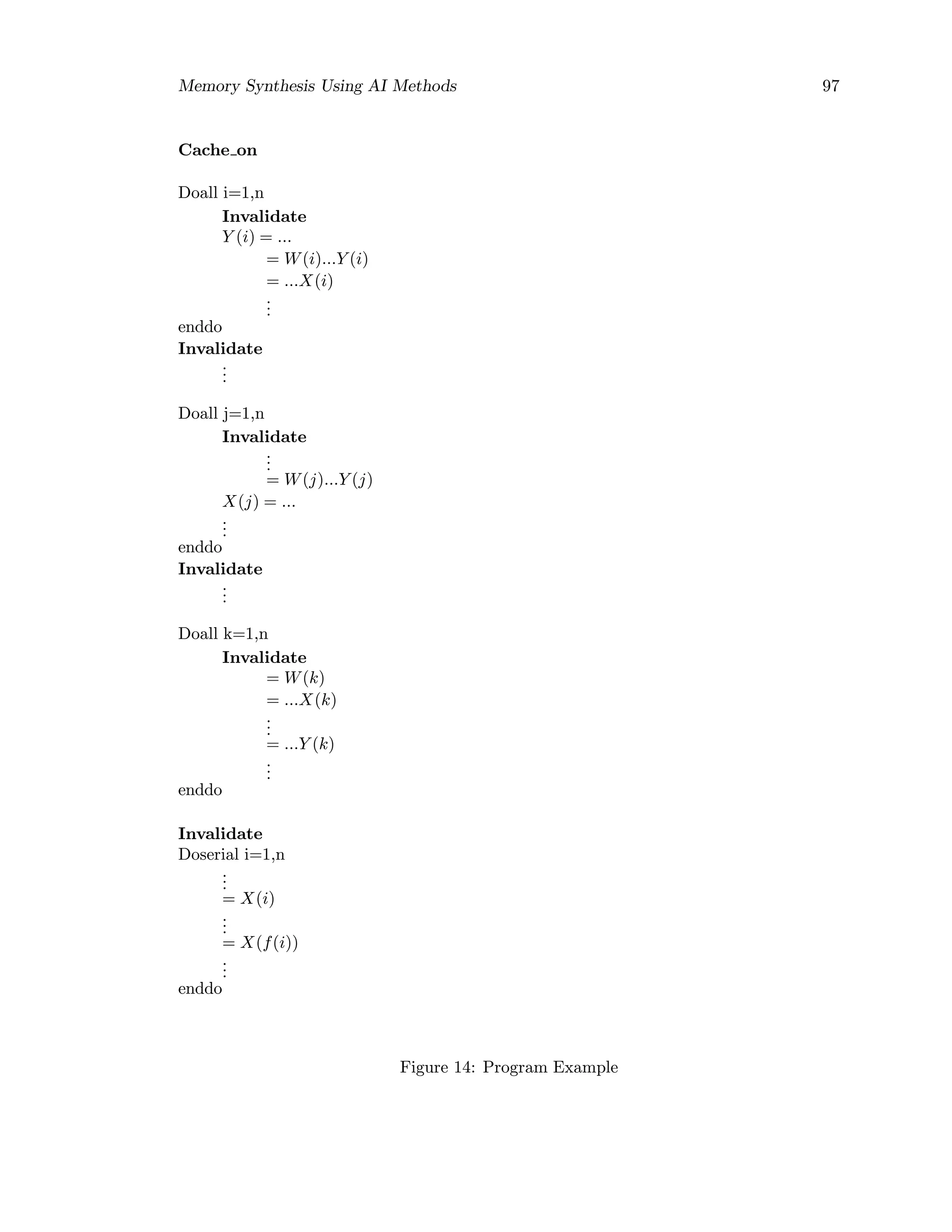
![Memory Synthesis Using AI Methods 99
10 MEMORY SYSTEM DESIGN AS A SYNERGY
10.1 Computer design requirements
Computer architects must design a computer to meet functional as well as price and
performance goals. Often, they also have to determine what the functional requirements
are, and this can be a major task. The requirements may be specific features, inspired
by the market. For example, the presence of a large market for a particular class of
applications might encourage the designers to incorporate requirements that would make
the machine competitive in that market. A classification of the functional requirements
that need to be considered ([6]) when a machine is designed:
Application area —this aspect refers to the target of the computer:
• Special purpose : typical feature is higher performance for specific applications;
• General purpose : typical feature is balanced performance for a range of tasks;
• Scientific : typical feature is high-performance for floating point;
• Commercial : typical features are support for data bases, transaction processing and
decimal aritmetic.
Level of software compatibility —this aspect determines the amount of existing soft-
ware for the machine:
• At programming language : this type of compatibility is the most flexible for designer
but requires new compilers;
• Object code or binary compatible: in this type of compatibility, the architecture
is completely defined —little flexibility— but no investment needed in software or
porting programs.
Operating system requirements — the necessary features to support a particular
operating system (OS) include:
• Size of address space : this is a very important feature; it may limit applications;
• Memory management : it may be flat, paged, segmented;
• Protection: the OS and applications may have different needs: page versus seg-
mented protection;
• Context switch : this feature supports process interrupt and restart;
• Interrupts and traps : the type of support for this features has impact on hardware
design and OS.](https://image.slidesharecdn.com/memorysynthesisusingaimethods-201006184613/75/Memory-synthesis-using_ai_methods-105-2048.jpg)
![Memory Synthesis Using AI Methods 101
10.2 General Memory Design Rules
In designing the memory hierarchy, one should take into account the pertaining rules of
thumb. These are [6]:
1. Amdahl/Case Rule: A balanced computer system needs about 1 megabyte of main
memory capacity and 1 megabit per second of I/O bandwidth per MIPS of CPU perfor-
mance.
2. 90/10 Locality Rule: A program executes about 90% of its instructions in 10% of its
code.
3. Address-Consumption Rule: The memory needed by the average program grows by
about a factor of 1.5 to 2 per year; thus, it consumes between 1/2 and 1 address bit per
year.
4. 90/50 Branch-Taken Rule: About 90% of backward-going branches are taken while
about 50% of forward-going branches are taken.
5. 2:1 Cache Rule: The miss ratio of a direct-mapped cache of size X is about the same
as a 2-way set associative cache of size X/2.
6. DRAM-Grwoth Rule: Density increases by about 60% per year, quadrupling in 3 years.
7. Disk-Growth Rule: Density increases by about 25% per year, doubling in 3 years.
Two important remarks are worthwhile. The first is that the improvement in DRAM
capacity (approximately 60% per year) has been faster in the recent past than the im-
provement in CPU performance (which has been from 25% to 50% per year). The second
fact is that the increase in DRAM speed is much slower than the increase in DRAM
capacity, reaching about 7% per year (these data are from Hennessy and Patterson [6]).
10.3 Dependences Between System Components
The optimum solution to the memory system design results from a synergy between a
multiprocessor’s software and hardware components. Some dependences that should be
considered when designing the memory hierarchy are:
1. The memory-consistency model supported by an architecture directly affects the
comlexity of the programming model and the performance;
2. The correctness of a coherence protocol is a function of the memory consistency
model adopted by the architecture.
3. The implementation of a synchronization method influences the memory and coher-
ence traffic;
4. The cache organization, the replacement strategy, the write policy, and the coherence
protocol influence the memory traffic.](https://image.slidesharecdn.com/memorysynthesisusingaimethods-201006184613/75/Memory-synthesis-using_ai_methods-107-2048.jpg)
![Memory Synthesis Using AI Methods 105
10.4.3 Line Size and Cache Fetch Algorithm
The minimum line size is determined by the machine word length. The maximum line
size is limited by several factors such as: the miss rate, the memory bandwidth (which
determines the transfer time, and thereby the Miss penalty), and the impact of line size on
the performance of cache-coherent multiprocessors (Section 9.7). A larger line size reduces
the cost of the tag memory, T, as equation (46), Subsection 10.4.1, shows, where the line
size is 2j.
The line size influences other parameters in the following way:
1. increasing the line size decreases the compulsory misses (exploits spatial locality)
and increases the conflict misses (does not preserve temporal locality). Therefore,
for small line sizes increasing the line size is expected to decrease the miss rate —due
to spatial locality—, while for large line sizes increasing the line size is expected to
increase the miss ratio —because it does not preserve the temporal locality.
2. increasing the line size increases the miss penalty because the transfer time is in-
creasing.
3. increasing the line size decreases the cost of the Tag memory; the Tag overhead
becomes a smaller fraction of the total cost of the cache.
4. increasing the line size in multiprocessor architectures may increase the invalidation
overhead and may cause false data sharing if the compiler does not enforce that
different shared variables are located in different cache blocks (Section 9.7). On the
other side, because more information is invalidated at once for larger line size, the
frequency of the invalidations may decrease when the line size increases, but this is
depending in a large extent of the data sharing patterns (Section 9.3) and of the
compiler.
The first two effects of the line size must be considered together because they affect the
Average memory-access time (equation (15), Section 5.2). For example, Smith has found
([20]) that for the IBM 3033 (64-byte line, cache size 64 Kbyte) the line size that gives
the minimum miss rate lies in the range 128 to 256 bytes. The reason for which IBM
has chosen a line size of 64 bytes (which is not optimum with respect to the miss rate)
is almost certainly that the transmission time for longer lines increases the miss penalty,
and the main memory data path width required would be too large and therefore too
expensive. Measurements on different cache organizations and computer architectures
indicate ([6],[20]) that the lowest Average memory-access time is for line sizes ranging
from 8 to 64-bytes.
When choosing the line size for a multiprocessor architecture, the effect of the line size on
the overall traffic (that is, both data and coherence traffic) should be considered as well.
For example, A. Gupta and W. Weber have found ([14]) that for the DASH multiprocessor
architecture the line size that gives the minimum overall traffic is 32 bytes.
When some criteria (e.g., miss rate) point to using a larger line size and the transfer time](https://image.slidesharecdn.com/memorysynthesisusingaimethods-201006184613/75/Memory-synthesis-using_ai_methods-111-2048.jpg)
![106 Memory Synthesis Using AI Methods
affects significantly the miss penalty, then the methods explained in Sections 6.9 may be
used to improve main memory bandwidth.
The two available choices for cache fetch are demand fetching and prefetching. The purpose
of prefetching (Section 6.5) is to reduce the miss rate for reads. However, prefecting
introduces some penalties: it increases the memory traffic and introduces cache lookup
accesses. The major factor in determining whether prefetching is useful is the line size.
Small line sizes generally result in a benefit from prefetching, while large line sizes lead
to the ineffectiveness of prefetching. The reason for this is that when the line is large, a
prefetch brings in a great deal of information, much or all of which may not be needed,
and removes an equally large amount of information, some of which may still be in use.
Smith ([20]) has found that for line sizes greater than 256 bytes prefetching brings no
improvement. The fastest hardware implementation of prefetching is provided by one
block lookahead (OBL) prefetch. Always prefetch provides a greater decrease in miss
ratio than prefetch on misses, but introduces also a greater memory and cache overhead.
As shown in Section 6.5, special steps must be taken to keep prefetching interference with
normal program accesses at an acceptable level.
As a general rule, one-block-lookahead prefetch with a line size of L bytes is a better
choice than demand fetch with a line size 2L bytes, because the former choice allows the
processor to proceed while the bytes L + 1 . . . 2L are fetched.
10.4.4 Line Replacement Strategy
Cache-line replacement strategy affects the miss rate and the memory traffic. The two
candidate choices are random, and LRU (or its approximation) replacement. FIFO re-
placement is not considered as a good choice because it has been shown to generally
perform poorer than random and its hardware cost is greater than that of random. The
replacement policy plays a greater role in smaller caches than in larger caches where there
are more choices of what to replace. Although LRU performs better than random, its edge
over random from the point of view of miss rate is less significant for large cache size and
the virtue of random of being simple to build in hardware may become more important.
LRU is the best choice for small and medium size caches because it preserves temporal
locality.
10.4.5 Write Strategy
For uniprocessor architectures, either write through or write back can be used. Write back
usually makes fetch-on-write — with the hope that the written line will be referenced again
soon, either by write or read accesses—, while write through usually does not make write
allocate — with the purpose of keeping room in the cache for data that is read and because
the subsequent writes to that block still have to go to memory. Using write through for
uniprocessors simplifies the cache-coherence problem for I/O because with this policy the
memory has an up-to-date copy of information and special schemes must be used to prevent
inconsistency only for I/O input but not for output (as shown in Subsection 5.13.1).](https://image.slidesharecdn.com/memorysynthesisusingaimethods-201006184613/75/Memory-synthesis-using_ai_methods-112-2048.jpg)

This document summarizes the research goals and findings of developing an intelligent design assistant for memory synthesis using AI methods. It discusses the growing performance gap between processors and main memory, and how memory hierarchy addresses this by organizing memory into faster, smaller, more expensive levels. The document outlines the knowledge acquisition and domain knowledge required for the memory synthesis tool, including topics like cache organization, memory protocols, consistency models, and optimizing overall memory system design.


![Vibe Coding vs. Spec-Driven Development [Free Meetup]](https://cdn.slidesharecdn.com/ss_thumbnails/vibecodingvsspecdrivendevelopment-251209105622-43f455e7-thumbnail.jpg?width=640&height=640&fit=bounds)


