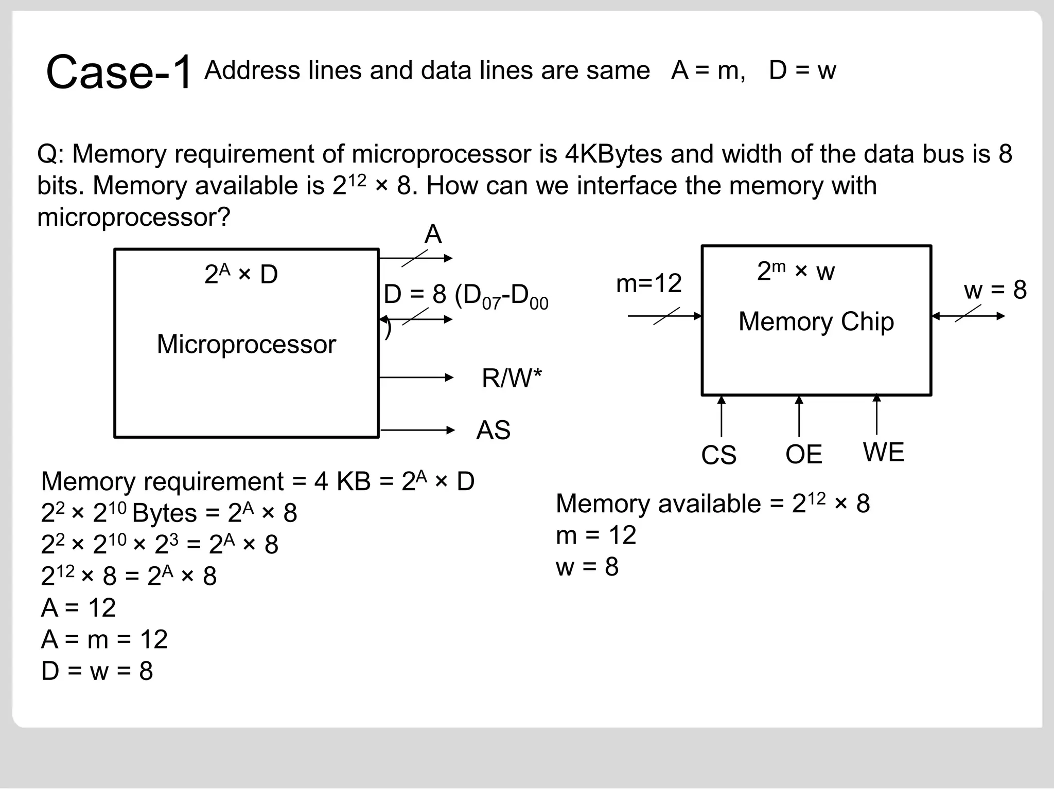
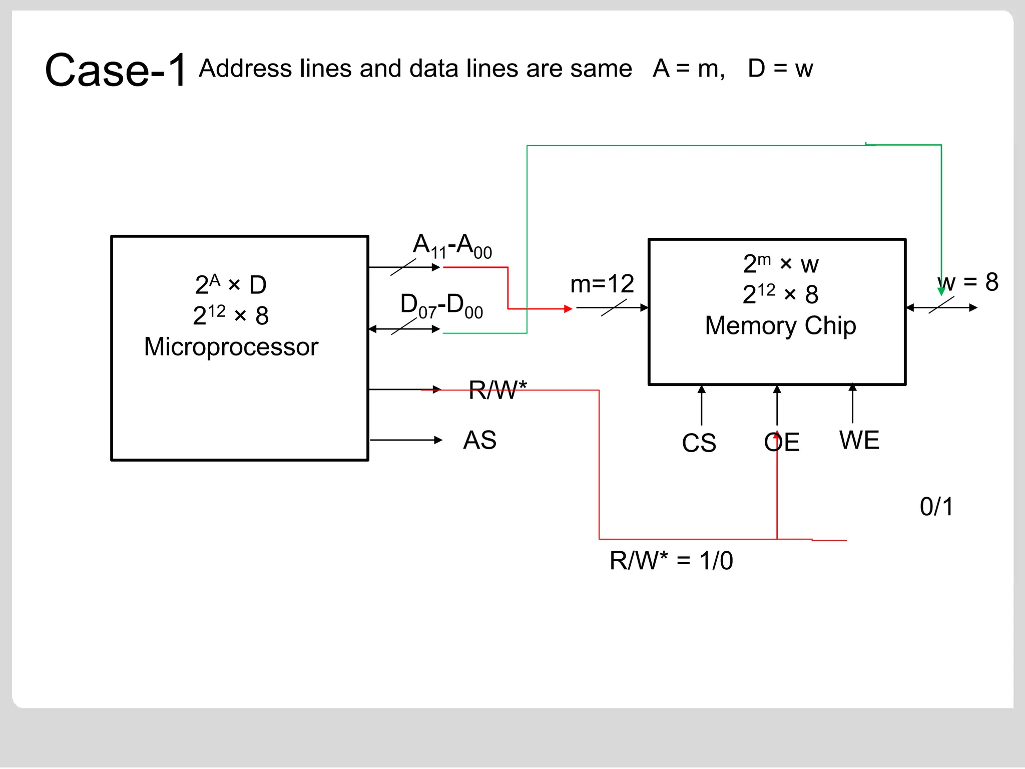
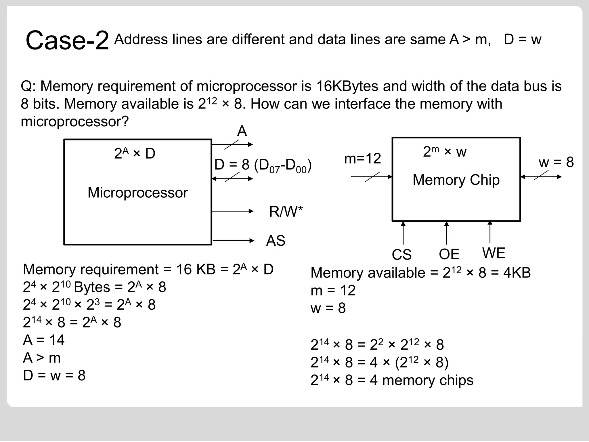
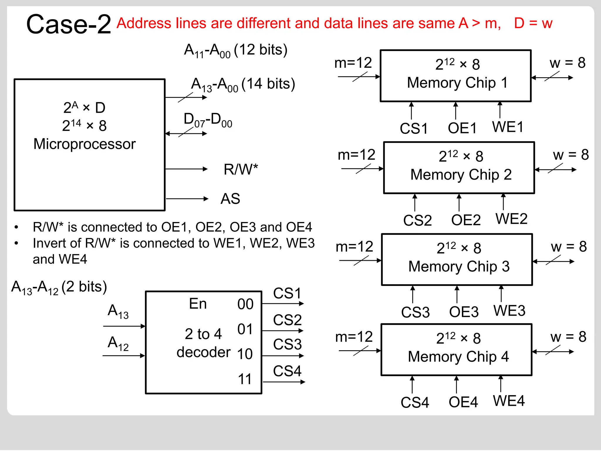
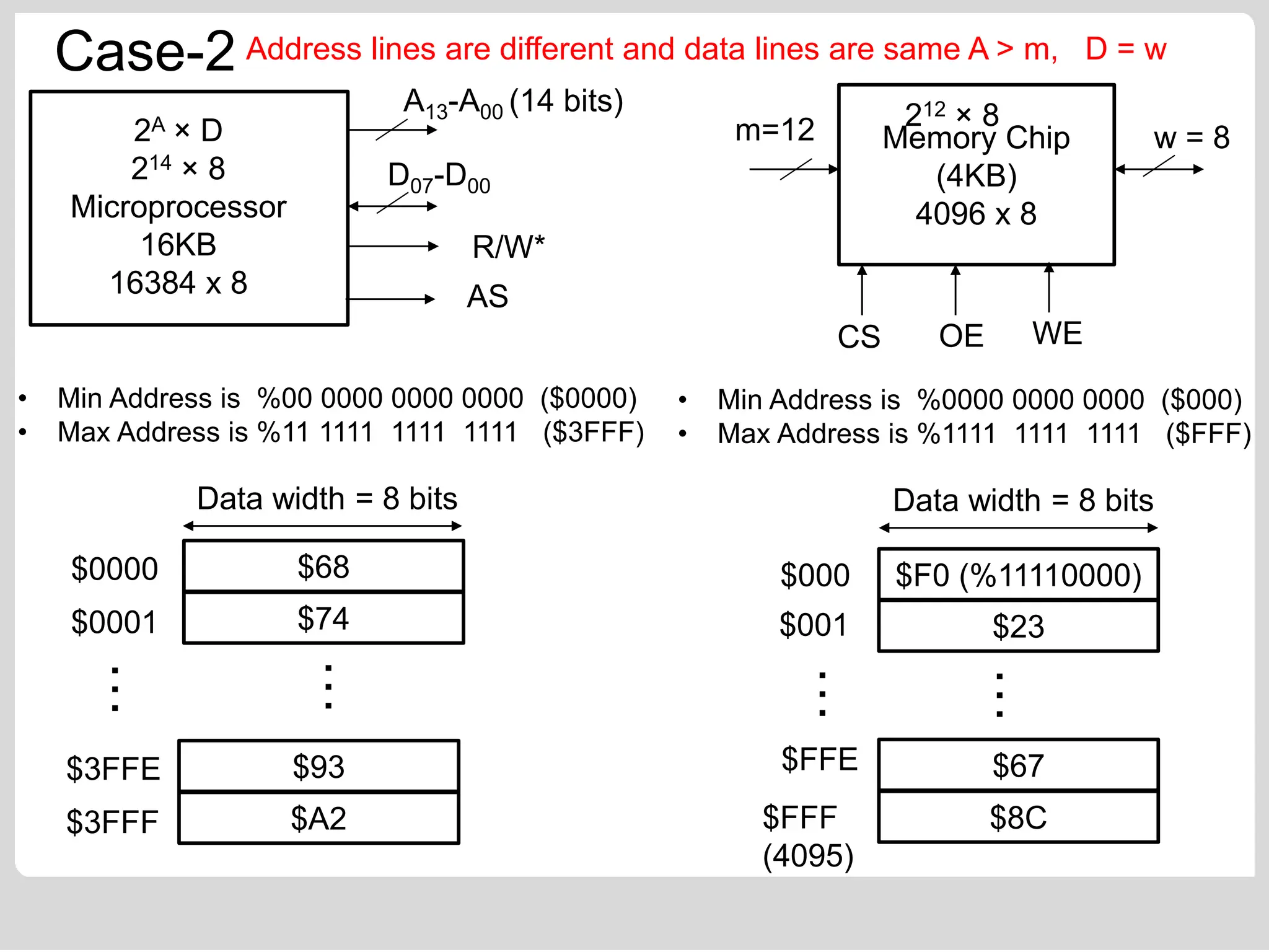
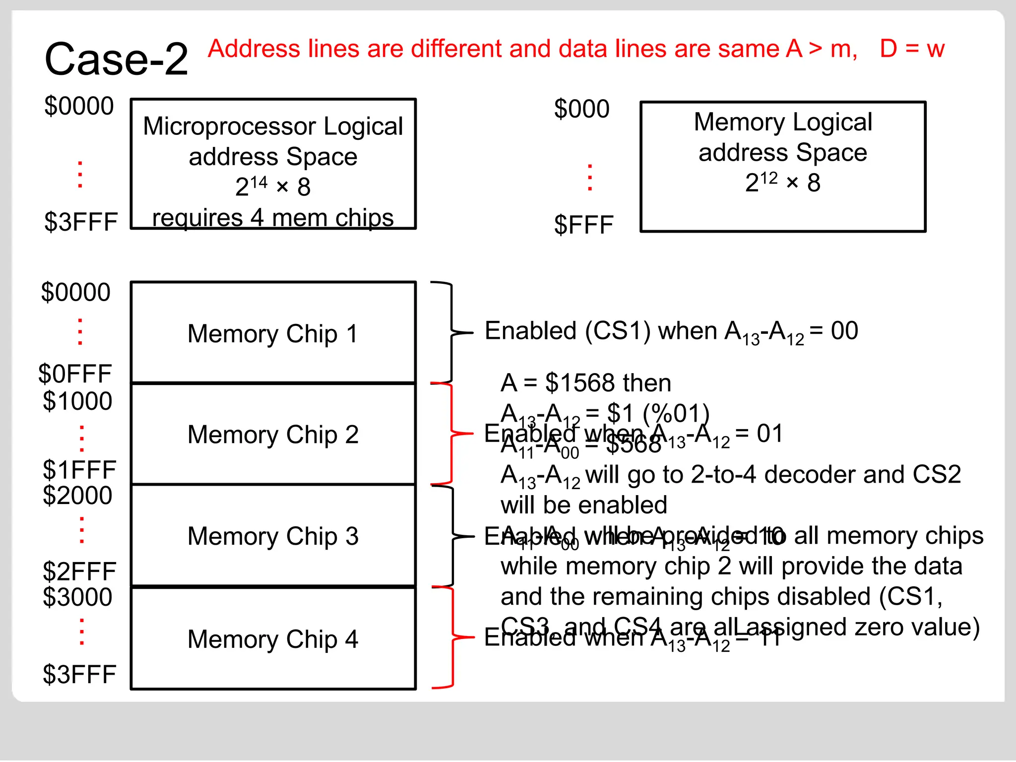
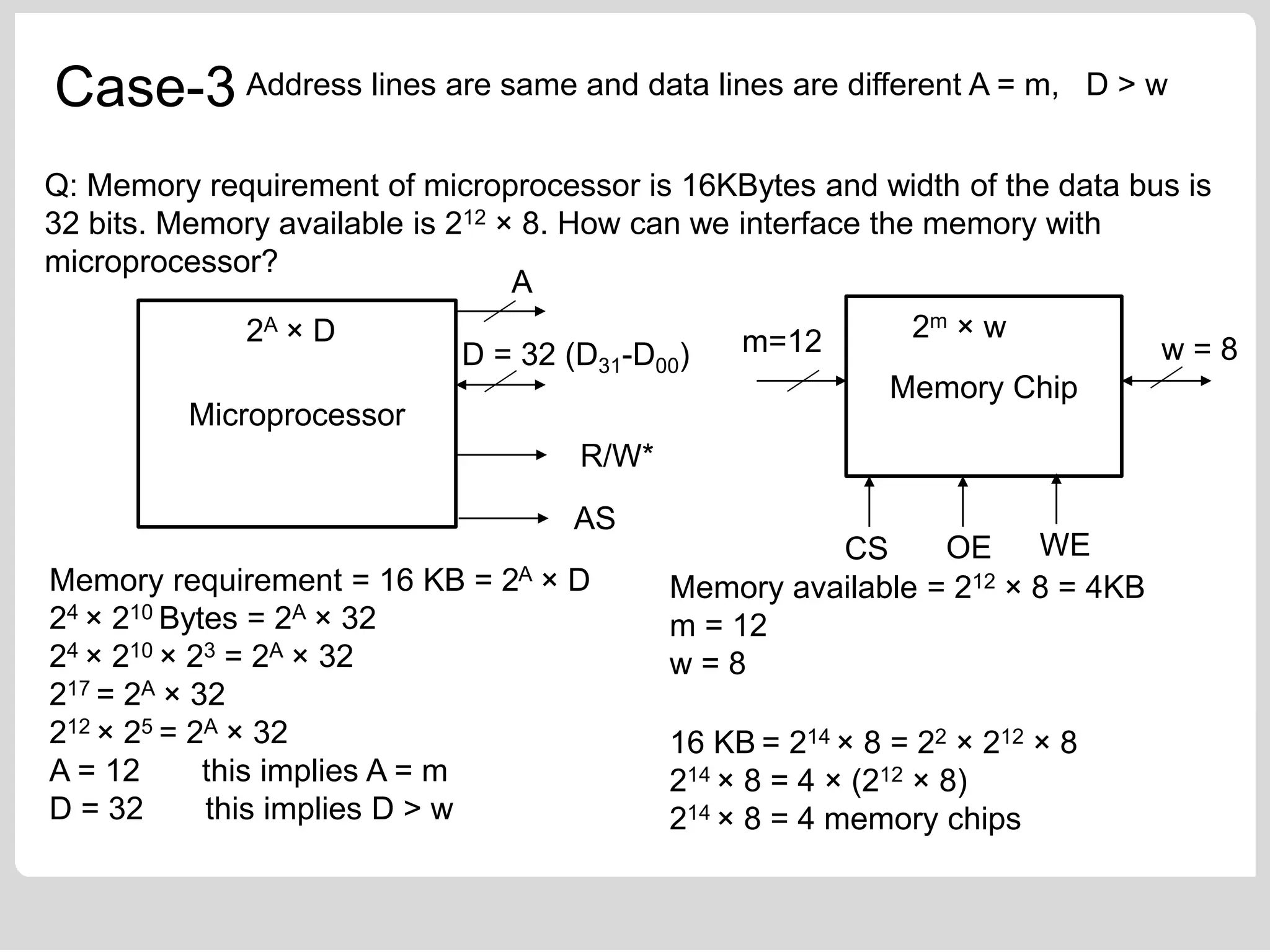
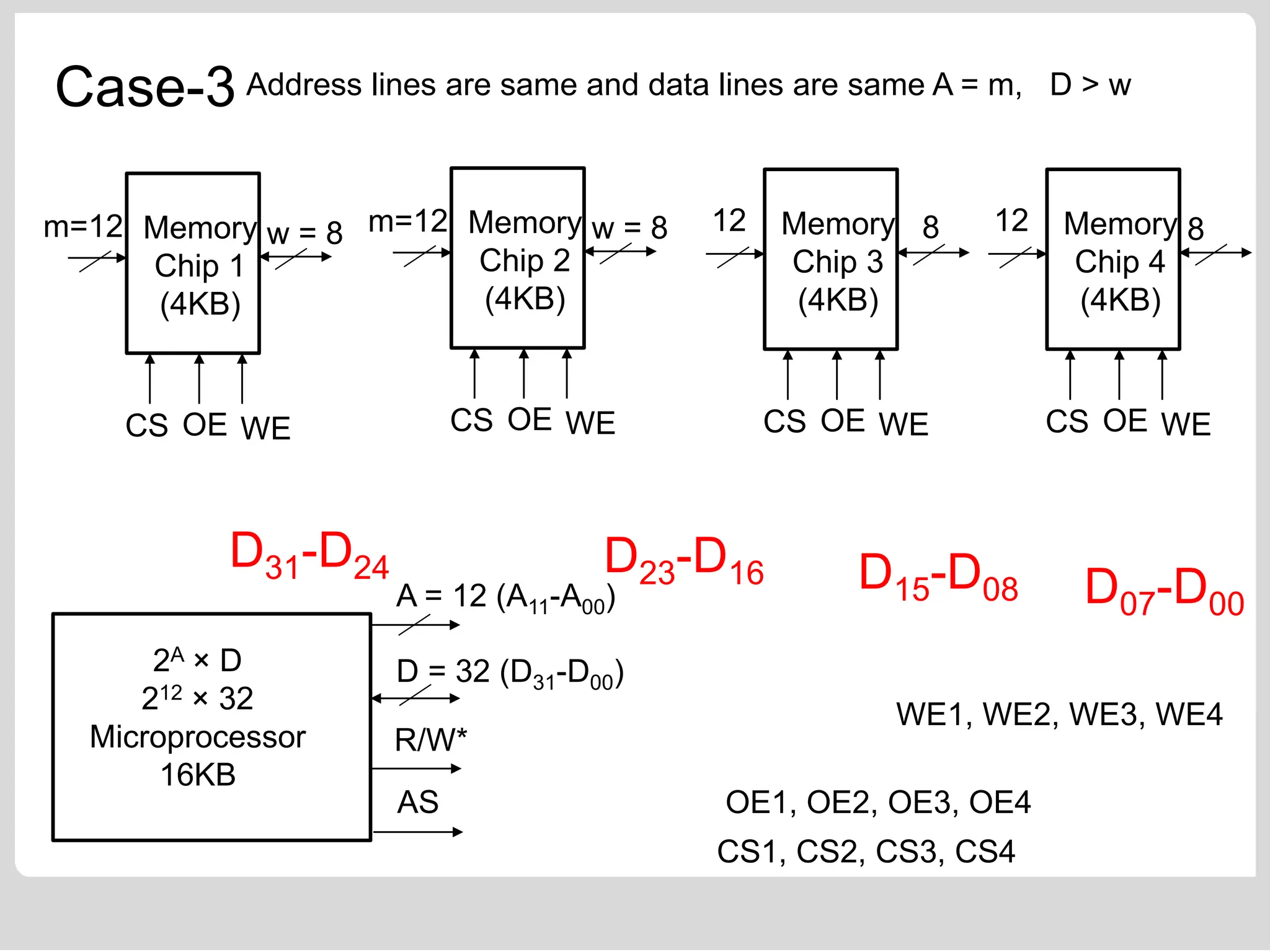
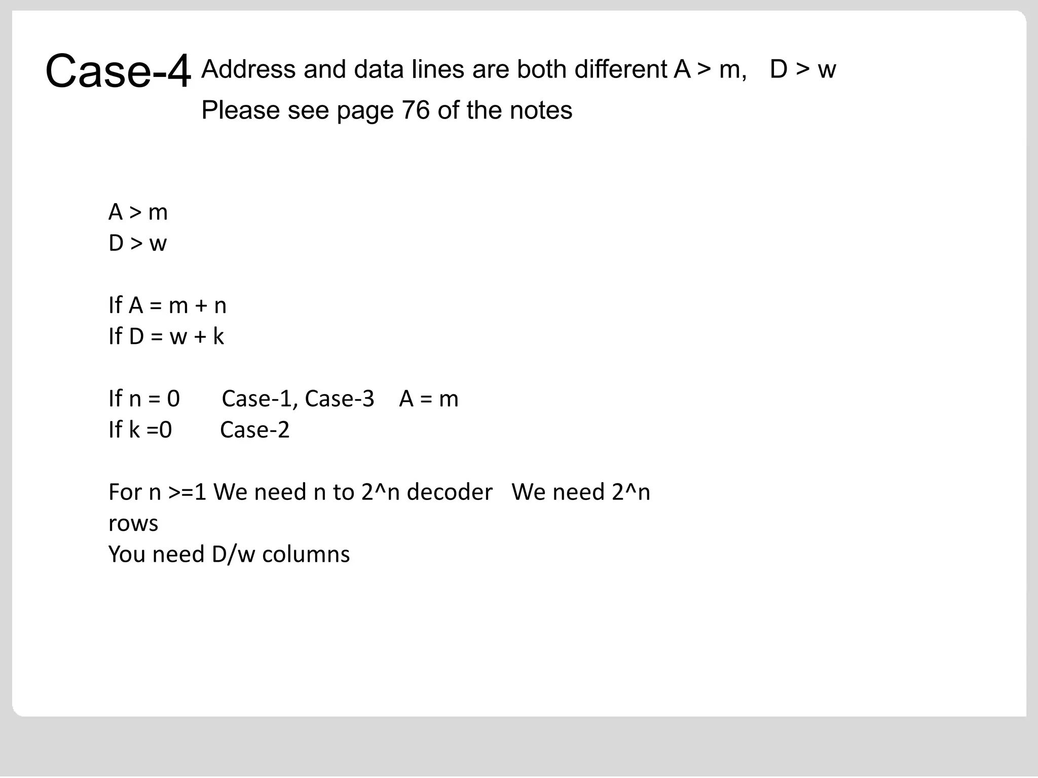
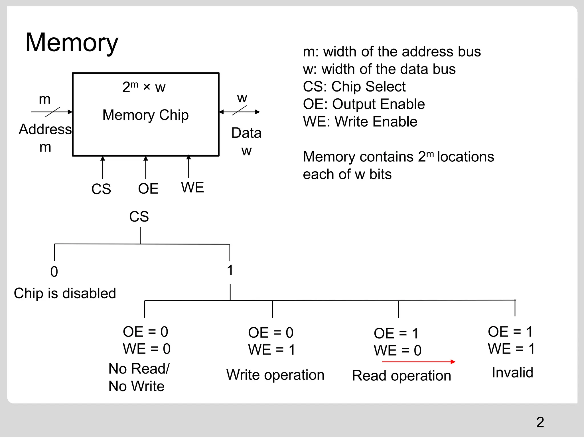
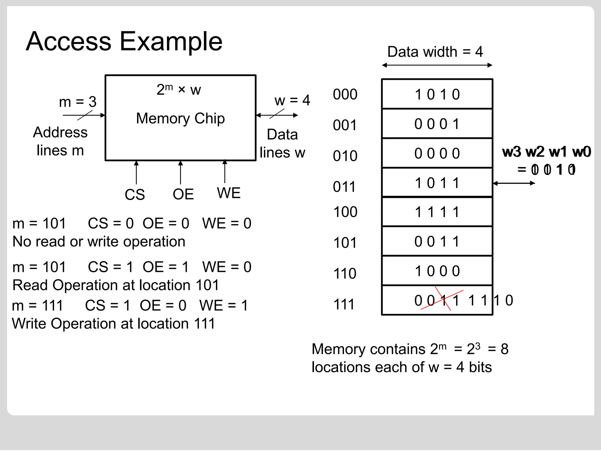
The document provides a detailed analysis of memory system design, focusing on memory chips and their interfacing with a microprocessor through various operational states like read and write. It outlines the requirements and configurations needed for specific memory sizes and bus widths, highlighting different cases where address and data lines correspond or differ. Examples are given for interfacing memory with microprocessors based on chip select and enable signals, using logical address spaces for effective memory management.
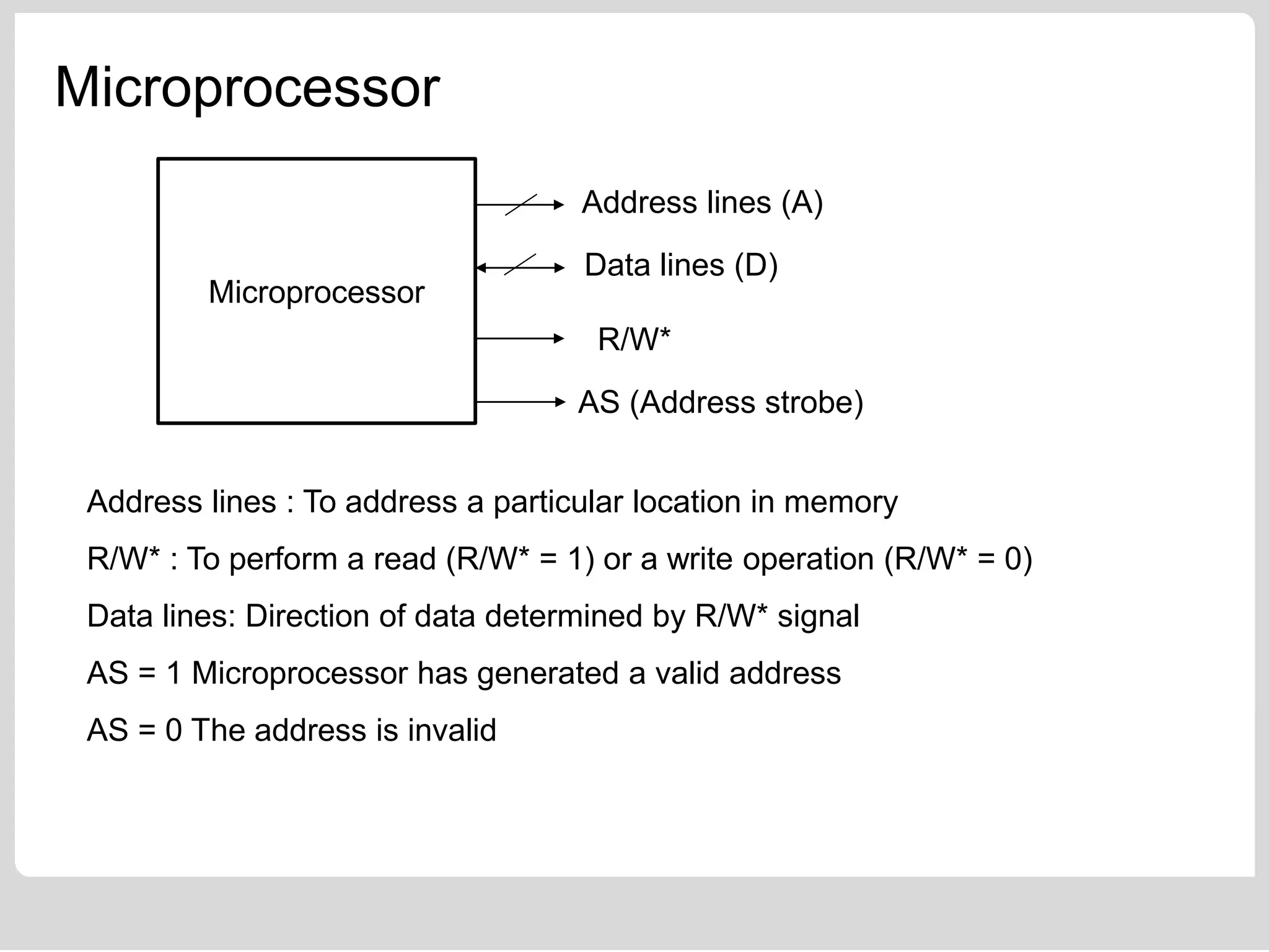
![Microprocessor (Instruction Fetch)
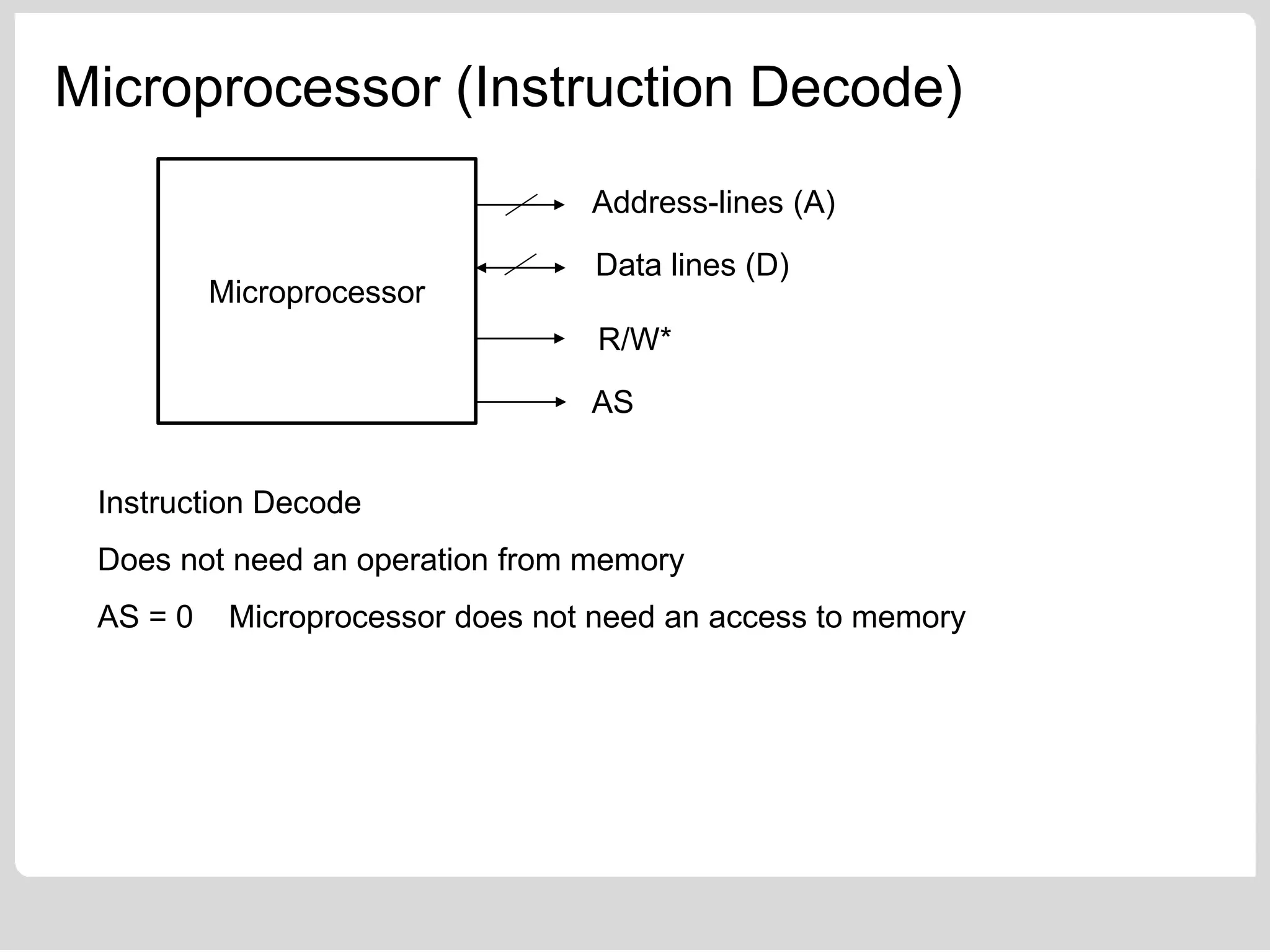
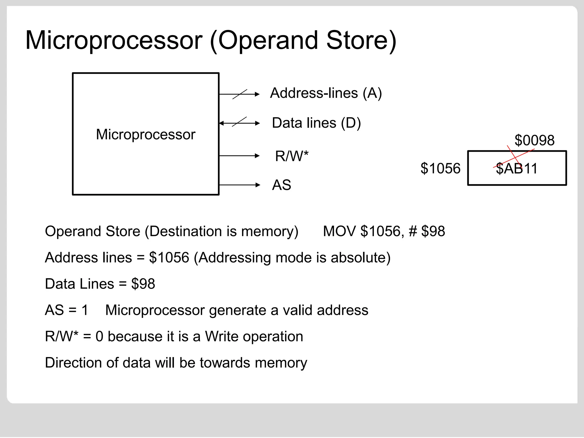
Microprocessor
Address-lines (A)
Data lines (D)
R/W*
AS
Instruction Fetch
Read Operation (AS = 1, R/W* = 1)
Address-lines = [MAR] which is loaded with PC address
Data-lines = Content of memory at location specified by address](https://image.slidesharecdn.com/memorydesign-240605190431-248b46a0/75/Memory-Design-of-embedded-system-engineering-pptx-5-2048.jpg)