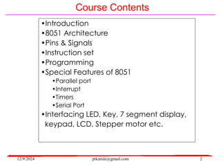
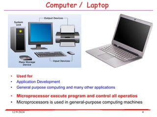
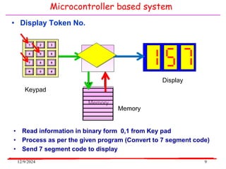
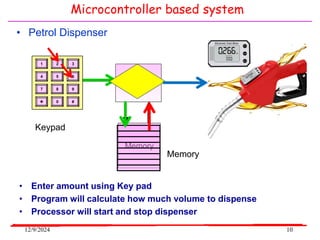
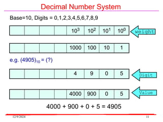
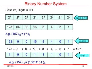
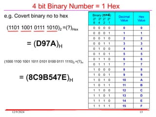
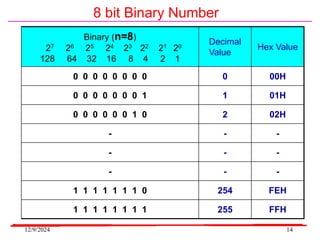
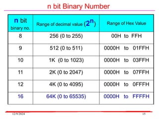
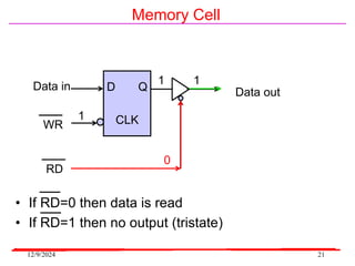
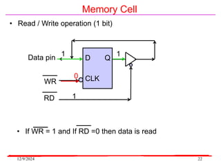
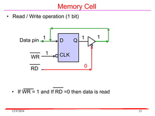
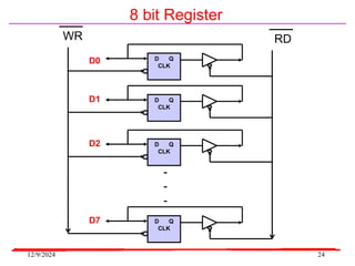
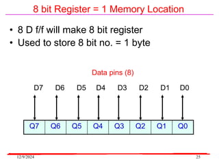
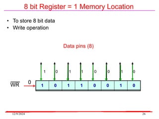
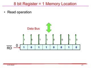
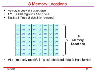
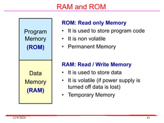
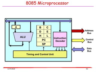
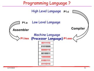
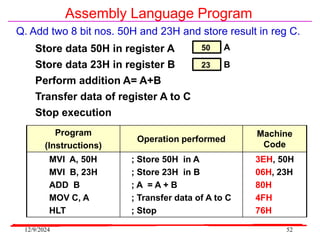
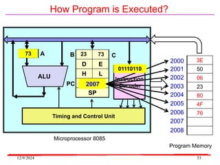
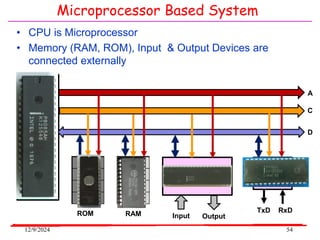
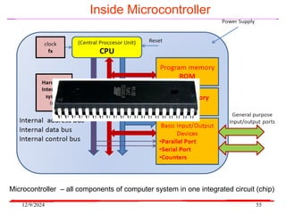
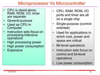
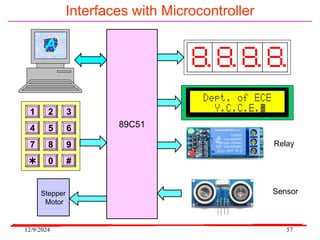
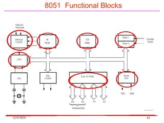
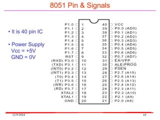
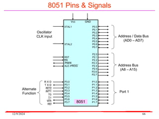
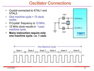
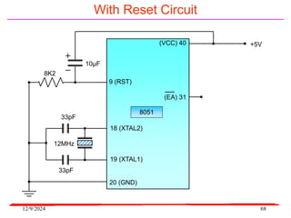
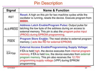
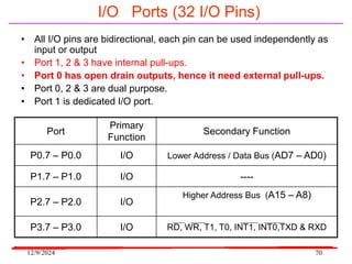
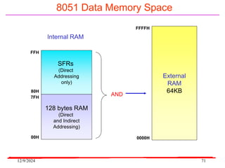
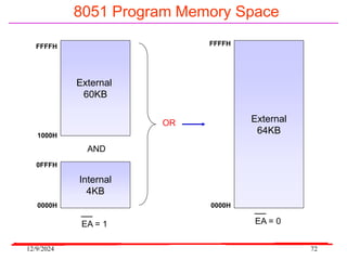
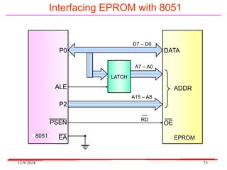
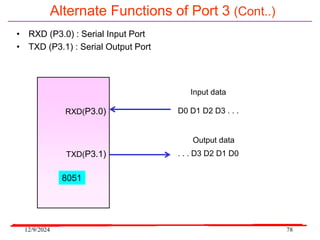
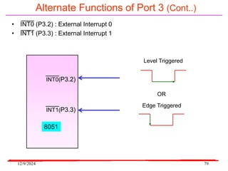
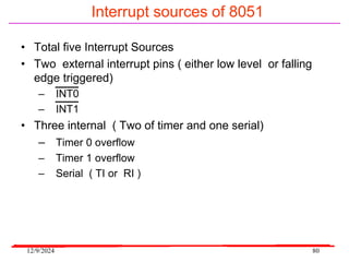
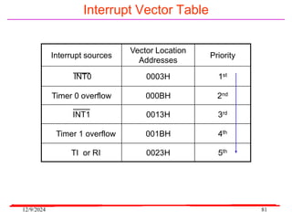
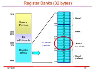
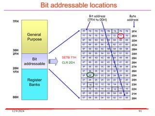
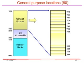
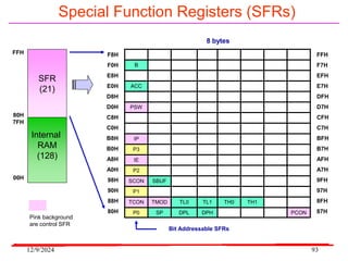
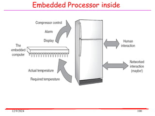
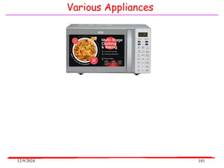
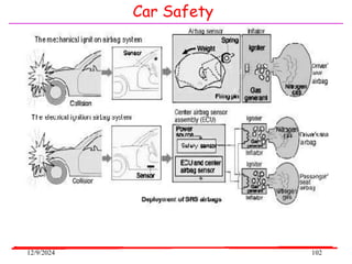
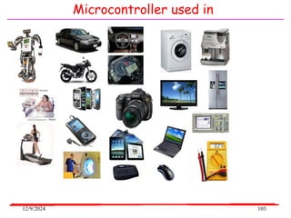
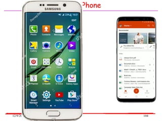
YCCE, Nagpur MGI
Microcontroller & its Applications
Dr. P. T. Karule
Professor
Department of Electronics Engineering
Yeshwantrao Chavan College of Engineering, Nagpur (M. S.)
Email: ptkarule@gmail.com, 412@ycce.in
Website: www.ycce.edu
8051 Microcontroller
12/9/2024 ptkarule@gmail.com 2
Course Contents
•Introduction
•8051 Architecture
•Pins & Signals
•Instruction set
•Programming
•Special Features of 8051
•Parallel port
•Interrupt
•Timers
•Serial Port
•Interfacing LED, Key, 7 segment display,
keypad, LCD, Stepper motor etc.
12/9/2024 3
Introduction of Microprocessor
12/9/2024 4
Computer / Laptop
• Microprocessor execute program and control all operatios
• Microprocessors is used in general-purpose computing machines
• Used for
• Application Development
• General purpose computing and many other applications
12/9/2024 5
Microcontroller used in
• Microcontroller inside
• Microcontroller used for specific application (products)
12/9/2024 6
Mobile Phone  Smart Phone
• Embedded Processor inside (with RTOS)
• Audio, Video Call, Digital Camera, Sharing Documents
• Many Applications – Online Payment, Bookings, Social media, Control,
Monitoring data, Gaming etc…
• Business Applications – Zomato, Swiggy, OLA, Uber
Mobile Phones Smart Phones
12/9/2024 7
Let’s Understand
Microcomputer ?
Memory?
Microprocessor?
Microcontroller?
12/9/2024 8
• Micro-computer ?
– CPU + Input Devices + Output Devices + Memory
e.g. Monitor
CPU
Memory
Input
Device
Output
Device
e.g. Keyboard
ROM - Program Memory
• CPU
– It is essentially a microprocessor
RAM - Data Memory
Microprocessor based system
12/9/2024 9
Microcontroller based system
• Display Token No.
Display
CPU
Memory
Input
Device
Output
Device
Keypad
Memory
3
2
1
6
5
4
9
8
7
#
0

• Read information in binary form 0,1 from Key pad
• Process as per the given program (Convert to 7 segment code)
• Send 7 segment code to display
12/9/2024 10
• Petrol Dispenser
CPU
Memory
Input
Device
Keypad
Memory
3
2
1
6
5
4
9
8
7
#
0

• Enter amount using Key pad
• Program will calculate how much volume to dispense
• Processor will start and stop dispenser
Microcontroller based system
12/9/2024 11
Decimal Number System
Base=10, Digits = 0,1,2,3,4,5,6,7,8,9
weight
Digit
103 102 101 100
1000 100 10 1
4 9 0 5
4000 900 0 5 Value
4000 + 900 + 0 + 5 = 4905
e.g. (4905)10 = (?)
12/9/2024 12
Binary Number System
Base=2, Digits = 0,1
weight
Digit
27 26 25 24 23 22 21 20
128 64 32 16 8 4 2 1
1 0 0 1 1 1 0 1
128 0 0 16 8 4 0 1 Value
128 + 0 + 0 + 16 + 8 + 4 + 0 + 1 = 157
e.g. (157)10 = (? )2
e.g. (157)10 = (10011101 )2
12/9/2024 13
4 bit Binary Number = 1 Hex
Binary (n=4)
23 22 21 20
8 4 2 1
Decimal
Value
Hex
Value
0 0 0 0 0 0
0 0 0 1 1 1
0 0 1 0 2 2
0 0 1 1 3 3
0 1 0 0 4 4
0 1 0 1 5 5
0 1 1 0 6 6
0 1 1 1 7 7
1 0 0 0 8 8
1 0 0 1 9 9
1 0 1 0 10 A
1 0 1 1 11 B
1 1 0 0 12 C
1 1 0 1 13 D
1 1 1 0 14 E
1 1 1 1 15 F
(1101 1001 0111 1010)2 =(?)Hex
= (D97A)H
e.g. Covert binary no to hex
(1000 1100 1001 1011 0101 0100 0111 1110)2 =(?)H
= (8C9B547E)H
12/9/2024 14
Binary (n=8)
27 26 25 24 23 22 21 20
128 64 32 16 8 4 2 1
Decimal
Value
Hex Value
0 0 0 0 0 0 0 0 0 00H
0 0 0 0 0 0 0 1 1 01H
0 0 0 0 0 0 1 0 2 02H
- - -
- - -
- - -
1 1 1 1 1 1 1 0 254 FEH
1 1 1 1 1 1 1 1 255 FFH
8 bit Binary Number
12/9/2024 15
n bit
binary no.
Range of decimal value (2n) Range of Hex Value
8 256 (0 to 255) 00H to FFH
9 512 (0 to 511) 0000H to 01FFH
10 1K (0 to 1023) 0000H to 03FFH
11 2K (0 to 2047) 0000H to 07FFH
12 4K (0 to 4095) 0000H to 0FFFH
16 64K (0 to 65535) 0000H to FFFFH
n bit Binary Number
12/9/2024 16
Memory ?
12/9/2024 17
Memory
00111110
01010000
00000110
(64K
bytes)
00111110
01010000
00000110
Memory is used
• to store Data
• to store Program
• in the form of 8 bit binary nos.
• 8 bit = 1 byte
12/9/2024 18
Memory Cell
• If CLK = 0 then data is stored
• If CLK = 1 then no change
D Q
CLK
CLK D Q
1 x NC
0 0 0
0 1 1
• The basic memory unit is D flip flop
• Used to store 1 bit data
12/9/2024 19
Memory Cell
Data in
WR
D Q
CLK
CLK D Q
1 x NC
0 0 0
0 1 1
• D = 1 then Q = 1
0
1 1
• If WR=0 then data is stored
12/9/2024 20
Memory Cell
• If WR=0 then data is stored
Data in
WR
D Q
CLK
CLK D Q
1 x NC
0 0 0
0 1 1
0
0 0 1
• D = 0 then Q = 0
X
12/9/2024 21
Memory Cell
Data in
WR
D Q
CLK
RD
Data out
0
1
1 1
• If RD=0 then data is read
• If RD=1 then no output (tristate)
12/9/2024 22
Memory Cell
• Read / Write operation (1 bit)
Data pin
WR
D Q
CLK
RD
• If WR = 1 and If RD =0 then data is read
0
1
1
1
12/9/2024 23
Memory Cell
• Read / Write operation (1 bit)
Data pin
WR
D Q
CLK
RD
• If WR = 1 and If RD =0 then data is read
0
1
1
1
1
12/9/2024 24
8 bit Register
D Q
CLK
D0
D Q
CLK
D1
D Q
CLK
D2
D Q
CLK
D7
WR RD
-
-
-
12/9/2024 25
8 bit Register = 1 Memory Location
• 8 D f/f will make 8 bit register
• Used to store 8 bit no. = 1 byte
Q7 Q6 Q5 Q4 Q3 Q2 Q1 Q0
D7 D6 D5 D4 D3 D2 D1 D0
Data pins (8)
12/9/2024 26
8 bit Register = 1 Memory Location
• To store 8 bit data
• Write operation
Data pins (8)
WR
1 0 1 1 0 0 1 0
0
1 0 1 1 0 0 1 0
12/9/2024 27
8 bit Register = 1 Memory Location
• Read operation
Data Bus
RD
0
1 0 1 1 0 0 1 0
1 0 1 1 0 0 1 0
12/9/2024 28
8 Memory Locations
Q0
Q1
Q2
Q3
Q4
Q5
Q6
Q7
Q0
Q1
Q2
Q3
Q4
Q5
Q6
Q7
Q0
Q1
Q2
Q3
Q4
Q5
Q6
Q7
Q0
Q1
Q2
Q3
Q4
Q5
Q6
Q7
Q0
Q1
Q2
Q3
Q4
Q5
Q6
Q7
Q0
Q1
Q2
Q3
Q4
Q5
Q6
Q7
Q0
Q1
Q2
Q3
Q4
Q5
Q6
Q7
Q0
Q1
Q2
Q3
Q4
Q5
Q6
Q7
8
Memory
Locations
• At a time only one M. L. is selected and data is transferred
• Memory is array of 8 bit registers
• 1 M.L. = 8 bit register = 1 byte data
• E.g. 8 x 8 (Array of eight 8 bit registers)
12/9/2024 29
8 Memory Locations
Address
(n bit)
• n bit address is used to select one memory location out
of 2n Memory Locations
• e.g. RAM 8 x 8
Data bus
000
001
010
011
100
101
110
111
8 bit
3
2n
Memory
Locations
00111110
01010000
00000110
00100011
10000000
01001111
01110110
01010101
12/9/2024 30
Address Decoder
• Memory IC consist of
• Register array as memory
• Address decoder to select one M.L.
3 x 8
address
decoder
3 bit
addr
A0
A1
A2
Y0
Y1
Y2
Y3
Y4
Y5
Y6
Y7
A2 A1 A0 Y7Y6Y5Y4Y3Y2Y1Y0
0 0 0 0 0 0 0 0 0 0 1
0 0 1 0 0 0 0 0 0 1 0
0 1 0 0 0 0 0 0 1 0 0
0 1 1 0 0 0 0 1 0 0 0
1 0 0 0 0 0 1 0 0 0 0
1 0 1 0 0 1 0 0 0 0 0
1 1 0 0 1 0 0 0 0 0 0
1 1 1 1 0 0 0 0 0 0 0
12/9/2024 31
Address Decoder
• Memory IC consist of
• Register array as memory
• Address decoder to select one M.L.
3 x 8
address
decoder
A0
A1
A2
Y0
Y1
Y2
Y3
Y4
Y5
Y6
Y7
1
0
0
0
1
0
0
0
0
0
0
12/9/2024 32
Address Decoder
• Memory IC consist of
• Register array as memory
• Address decoder to select one M.L.
3 x 8
address
decoder
A0
A1
A2
Y0
Y1
Y2
Y3
Y4
Y5
Y6
Y7
1
0
1
0
0
0
0
0
1
0
0
12/9/2024 33
8 Memory Locations IC
• Memory IC consist of
• Register array as memory
• Address decoder to select one M.L.
3 x 8
address
decoder
A0
A1
A2
Y0
Y1
Y2
Y3
Y4
Y5
Y6
Y7
1
0
0
00111110
01010000
00000110
00100011
10000000
01001111
01110110
01010101
12/9/2024 34
RAM IC Internal
Address bus
(n bit)
CS
Data bus
(8 bit)
RAM IC
(2n x 8)
Addr
ess
De
coder
(n X 2n)
2n
Out
puts
EN
R/W Control
WR
RD
12/9/2024 35
Memory Capacity
No. of
address
pins (n)
No. of Memory Locations
present in RAM IC (2n)
Data Storage
Capacity
8 256 256 bytes
9 512 512 bytes
10 1K (1024) 1 K bytes
11 2K (2048) 2KB
16 64K (65536) 64KB
20 1M 1 MB
30 1G 1 GB
32 4G 4 GB
34 ? ?
12/9/2024 36
4 / 8 / 16 GB
Why not 10 GB / 20 GB ?
12/9/2024 37
e.g. RAM 1K X 8
EN
A9 – A0
CS
D7 – D0
RAM IC
(1K X 8)
Addr
ess
De
coder
(n X 2n)
1024
Out
puts
R/W Control
WR
RD
10
8
12/9/2024 38
e.g. RAM 64K X 8
EN
A15 – A0
CS
D7 – D0
RAM IC
(64K X 8)
Addr
ess
De
coder
(n X 2n)
64k
Out
puts
R/W Control
WR
RD
16
8
12/9/2024 39
12/9/2024 40
Memory Map
3E
50
06
(64KB
Data &
instruction
code)
23
80
4F
0000H
FFFFH
FFFEH
FFFDH
0002H
0001H
Data
(8 bit)
Address
(16 bit)
12/9/2024 41
RAM and ROM
Program
Memory
(ROM)
ROM: Read only Memory
• It is used to store program code
• It is non volatile
• Permanent Memory
RAM: Read / Write Memory
• It is used to store data
• It is volatile (if power supply is
turned off data is lost)
• Temporary Memory
Data
Memory
(RAM)
12/9/2024 42
Microprocessor ?
12/9/2024 43
What is Microprocessor?
• Microprocessor is a VLSI circuit, which
execute instructions of given program
sequentially.
• It read instruction code from memory,
instruction decoder decodes the code and
then it is executed.
• It generate control signals to read / write
data to / from I/O devices and Memory
12/9/2024 44
Microprocessor Evolution
12/9/2024 45
16 bit data bus (D15……..D0)
• e.g. 16 data = 5C74 H
• 16 bit long data is stored in 2 consecutive locations
74
5C
0000
0001
0002
0003
0004
0005
0006
0007
0008
74 0000
0002
0004
5C 0001
0003
0005
D7 ..D0
D15 ..D8
8 8
• 2 RAM IC are physically connected to processor
• 2 RAM IC are selected concurrently to read / write 16 bit data
12/9/2024 46
32 bit data bus (D31……..D0)
• e.g. 32 data = 123A55F4 H
• 32 bit long data is stored in 4 consecutive locations
F4
55
3A
12
0000
0001
0002
0003
0004
0005
0006
0007
0008
F4 0000
0004
0008
55 0001
0005
0009
3A 0002
0006
000A
12 0003
0007
000B
D7 ..D0
D15 ..D8
D23 ..D16
D31 ..D24
8 8 8 8
• 4 RAM IC are physically connected to processor
• 4 RAM IC are selected concurrently to read / write 32 bit data
64 bit data bus (D63……..D0)
12/9/2024 48
How many bit Processor?
ALU
• It depends on capacity of ALU
• Maximum size of operand (8/16/32/64 bit) used
to perform arithmetic or logical operation in a
instruction
• 8/16/32/64 bit processor
+, -, x, /…
12/9/2024 49
8085 Microprocessor
• The 8085 is 8 bit microprocessor developed by
Intel in 1976.
• It is 40 pin IC.
• It is having 8 bit data bus and 16 bit address
bus
• The 8085 contains.
– ALU
– 8 bit registers A, B, C, D, E, H, L
– 16 bit registers PC, SP
– Instruction Decoder
– Timing and Control Unit
12/9/2024 50
8085 Microprocessor
Instruction
Decoder
Timing and Control Unit
ALU
Data
Bus
Control
Bus
Address
Bus
A B C
D E
H L
PC
SP
12/9/2024 51
Programming Language ?
Compiler
Assembler
00111110
01010000
00000110
00100011
10000000
01001111
01110110
P1.exe
P1.c
P1.a
P1.hex
High Level Language
Low Level Language
Machine Language
(Processor Language)
12/9/2024 52
Assembly Language Program
Q. Add two 8 bit nos. 50H and 23H and store result in reg C.
Program
(Instructions)
Operation performed
Machine
Code
MVI A, 50H
MVI B, 23H
ADD B
MOV C, A
HLT
; Store 50H in A
; Store 23H in B
; A = A + B
; Transfer data of A to C
; Stop
3EH, 50H
06H, 23H
80H
4FH
76H
Store data 50H in register A
Store data 23H in register B
Perform addition A= A+B
Transfer data of register A to C
Stop execution
A
50
B
23
12/9/2024 53
How Program is Executed?
3E
50
06
23
80
4F
76
Instruction
Decoder
Timing and Control Unit
ALU
D E
H L
2000
SP
2000
2001
2002
2003
2004
2005
2006
2007
2008
B
A C
50 23
73 73
2001
2002
2003
2004
2005
2006
2007
00111110
00000110
10000000
01001111
01110110
PC
Program Memory
Microprocessor 8085
12/9/2024 54
Microprocessor Based System
• CPU is Microprocessor
• Memory (RAM, ROM), Input & Output Devices are
connected externally
8085
uP
D
C
A
Serial
Port
I / O
Ports
ROM Input Output
TxD RxD
RAM
12/9/2024 55
Inside Microcontroller
Microcontroller – all components of computer system in one integrated circuit (chip)
12/9/2024 56
Microprocessor Vs Microcontroller
• CPU is stand-alone,
RAM, ROM, I/O, timer
are separate
• General-purpose
• Used as CPU in
Computer
• Instruction sets focus on
processing-intensive
operations
• High processing power
• High power consumption
• Expensive
• CPU, RAM, ROM, I/O
ports and timer are all
on a single chip
• Single-purpose (control-
oriented)
• Used for applications in
which cost, power and
space are critical
• Bit-level operations
• Instruction sets focus on
control and bit-level
operations
• Low power consumption
12/9/2024 57
Interfaces with Microcontroller
89C51
3
2
1
6
5
4
9
8
7
#
0

Relay
Sensor
Stepper
Motor
12/9/2024 58
Where are microcontrollers used?
Microcontroller are used typically where processing
power is not critical.
• In household appliances like TV,DVD player, audio
system, washing machine,microwave etc.
• Micro controller applications are in office automation
industry
• In consumer electronics goods
• Used in communication and automobile market
• Wherever you need automation
• In hand held battery operated devices
12/9/2024 59
Advantages of using Microcontrollers
• Fast and effective
– The architecture correlates closely with the problem being solved
(control systems).
• Low cost / Low Power
– High level of system integration within one component only a
handful of components needed to create a working system.
• Compatibility
– Opcodes and binaries are the SAME for all 80x51 variants.
• Multi-sourced
– Over 12 manufacturers, hundreds of varieties.
• Constant improvement
– Improvements in silicon/design increase speed and power
annually.
• Good documentation
• Freely available development tools
YCCE, Nagpur MGI
8051 Microcontroller
Dr. P. T. Karule
Professor
Department of Electronics Engineering
Yeshwantrao Chavan College of Engineering, Nagpur (M. S.)
Email: ptkarule@gmail.com, 412@ycce.in
Website: www.ycce.edu
8051 Microcontroller
12/9/2024 61
8051 Microcontroller
• The 8051 is 8 bit microcontroller originally
developed by Intel in 1980.
• It is 40 pin IC.
• The 8051 contains.
– CPU with Boolean processor.
– 5 interrupts (2 external & 3 internal).
– 2, 16 bit timer/counter.
– Serial port.
– 32 I/O lines ( four 8- bit ports).
– 128 x 8 bit internal RAM.
– 4K x 8 ROM.
12/9/2024 62
8051 Functional Blocks
12/9/2024 63
Different Internal Blocks Description
• I/O Ports
– Four 8 bit I/O ports (P0,P1,P2 & P3), i.e. 32 I/O lines
• Timers
– Two 16 bit up counters, Timer0 and Timer1
– Can be used as timers or event counters
– Can interrupt 8051 internally after timeout
• Serial I/O
– Serial port with TXD and RXD pins can be used with RS232 bus for
communication with PC
• Interrupts
– Total 5 hardware interrupts
– Two external active low / edge triggered interrupts (INT0 & INT1)
– Three internal interrupts (From Timers & Serial I/O)
12/9/2024 64
8051 Pins and Signals
12/9/2024 65
8051 Pin & Signals
• It is 40 pin IC
• Power Supply
Vcc = +5V
GND = 0V
12/9/2024 66
8051 Pins & Signals
Vcc GND
XTAL1 P0.0
P0.1
P0.2
P0.3
P0.4
P0.5
XTAL2 P0.6
P0.7
P2.0
RST P2.1
EA P2.2
PSEN P2.3
ALE /PROG P2.4
P2.5
P2.6
P2.7
P3.0 P1.0
P3.1 P1.1
P3.2 P1.2
P3.3 P1.3
P3.4 P1.4
P3.5 P1.5
P3.6 P1.6
P3.7 P1.7
8051
Address / Data Bus
(AD0 – AD7)
Address Bus
(A8 – A15)
Port 1
R X D
T X D
INT0
INT1
T0
T1
WR
RD
Alternate
Function
Oscillator
CLK input
12/9/2024 67
Oscillator Connections
• Crystal connected to XTAL1 and
XTAL2.
• One machine cycle = 12 clock
cycles
• If Crystal frequency is 12 MHz.
• 12 MHz clock results in 1usec
machine cycle.
• Many instruction require only
one machine cycle. i.e. 1 usec
One Machine Cycle
18 (XTAL2)
19 (XTAL1)
33pF
33pF
12MHz
8051
State 1 State 2 State 6
State 5
State 4
State 3
12/9/2024 68
With Reset Circuit
(VCC) 40
9 (RST)
(EA) 31
18 (XTAL2)
19 (XTAL1)
20 (GND)
33pF
33pF
8K2
12MHz
10µF
8051
+5V
12/9/2024 69
Pin Description
Signal Name & Function
RST
Reset: A high on this pin for two machine cycles while the
oscillator is running, resets the device. Execute program from
0000H.
ALE/PROG
Address Latch Enable/Program Pulse: Output pulse for
latching the low byte of the address during an access to
external memory. This pin is also the program pulse input
(PROG) during EPROM programming.
PSEN
Program Store Enable: The read strobe to external program
memory. ( acts like RD for external EPROM)
EA/Vpp
External Access Enable/Programming Supply Voltage:
If EA is held high, the device executes from internal program
memory. If EA is held low, the device executes from external
program memory. This pin also receives the 12.75V
programming supply voltage (VPP) during EPROM
programming.
12/9/2024 70
I/O Ports (32 I/O Pins)
• All I/O pins are bidirectional, each pin can be used independently as
input or output
• Port 1, 2 & 3 have internal pull-ups.
• Port 0 has open drain outputs, hence it need external pull-ups.
• Port 0, 2 & 3 are dual purpose.
• Port 1 is dedicated I/O port.
Port
Primary
Function
Secondary Function
P0.7 – P0.0 I/O Lower Address / Data Bus (AD7 – AD0)
P1.7 – P1.0 I/O ----
P2.7 – P2.0 I/O
Higher Address Bus (A15 – A8)
P3.7 – P3.0 I/O RD, WR, T1, T0, INT1, INT0,TXD & RXD
12/9/2024 71
8051 Data Memory Space
External
RAM
64KB
FFFFH
0000H
AND
128 bytes RAM
(Direct
and Indirect
Addressing)
7FH
00H
Internal RAM
SFRs
(Direct
Addressing
only)
FFH
80H
12/9/2024 72
8051 Program Memory Space
AND
OR
Internal
4KB
EA = 1
0FFFH
0000H
EA = 0
External
64KB
FFFFH
0000H
External
60KB
FFFFH
1000H
12/9/2024 73
P0
ALE
P2
PSEN
EA
DATA
ADDR
OE
LATCH
8051 EPROM
Interfacing EPROM with 8051
D7 – D0
A7 – A0
A15 – A8
RD
12/9/2024 74
Interfacing RAM with 8051
P0
ALE
P2
RD
WR
EA
DATA
ADDR
OE
WE
LATCH
8051
with
internal ROM
RAM
Vcc
P3
D7 – D0
A7 – A0
A15 – A8
12/9/2024 75
Alternate Functions of Port 3
Port Pin Alternate Function
P3.0 RxD (Serial Input Port)
P3.1 TxD (Serial Output Port)
P3.2 INT0 ( External Interrupt 0)
P3.3 INT1 ( External Interrupt 1)
P3.4 T0 (Timer 0 External Input)
P3.5 T1 (Timer 1 External Input)
P3.6 WR ( External data memory write)
P3.7 RD ( External data memory read)
12/9/2024 76
Alternate Functions of Port 3 (Cont..)
• RD (P3.7) : External data memory read control signal
• WR (P3.6) : External data memory write control signal
RD(P3.7)
WR(P3.6)
8051
OE
WE
External
RAM
12/9/2024 77
Alternate Functions of Port 3 (Cont..)
• T0 (P3.4) : Timer 0 External input
• T1 (P3.5) : Timer 1 External input
T0(P3.4)
T1(P3.5)
8051
External CLK
12/9/2024 78
Alternate Functions of Port 3 (Cont..)
• RXD (P3.0) : Serial Input Port
• TXD (P3.1) : Serial Output Port
RXD(P3.0)
TXD(P3.1)
8051
Input data
D0 D1 D2 D3 . . .
Output data
. . . D3 D2 D1 D0
12/9/2024 79
Alternate Functions of Port 3 (Cont..)
• INT0 (P3.2) : External Interrupt 0
• INT1 (P3.3) : External Interrupt 1
INT0(P3.2)
INT1(P3.3)
8051
Level Triggered
Edge Triggered
OR
12/9/2024 80
Interrupt sources of 8051
• Total five Interrupt Sources
• Two external interrupt pins ( either low level or falling
edge triggered)
– INT0
– INT1
• Three internal ( Two of timer and one serial)
– Timer 0 overflow
– Timer 1 overflow
– Serial ( TI or RI )
12/9/2024 81
Interrupt Vector Table
Interrupt sources
Vector Location
Addresses
Priority
INT0 0003H 1st
Timer 0 overflow 000BH 2nd
INT1 0013H 3rd
Timer 1 overflow 001BH 4th
TI or RI 0023H 5th
12/9/2024 82
8051 Architecture
12/9/2024 83
8051 Architecture
12/9/2024 84
Port Drivers & Latches
12/9/2024 85
ALU
• ALU :-.
– 8 bit ALU used to perform addition, subtraction, increment,
decrement, multiplication & division.
– Logical operations like ANDing, Oring, XORing, Inverting, Rotating
& 1’s Complement.
– Boolean operations like bit Set, Reset, Complement,ANDing &
ORing.
• TMP1 & TMP2 :-.
– Temporary registers with ALU, can not be used by programmer.
• Accumulator (A) :–.
– 8 bit register used to perform arithmetic & logical operations. It is
also used transfer data to/from external memory.
• Register B :-.
– 8 bit register used for multiplication & division.
12/9/2024 86
PSW (Program status Word)
P
-
OV
RS0
RS1
F0
AC
CY
PSW.7 PSW.6 PSW.5 PSW.4 PSW.3 PSW.2 PSW.1 PSW.0
Flag Bit Name
CY PSW.7 Carry Flag
AC PSW.6 Auxiliary Carry Flag
F0 PSW.5 Flag 0 available for general purpose
RS1 PSW.4 Register Bank Selector Bit 1
RS0 PSW.3 Register Bank Selector Bit 0
OV PSW.2 Overflow Flag
P PSW.0 Parity Flag
12/9/2024 87
Register Bank Select Flags
The starting 32 locations of 128 bytes RAM are used as
register banks. The 32 locations are divided into 4 banks of
8 registers each R0 – R7. RS1 RS0 bits are used to select
any one out of 4 register banks.
RS1
(PSW.4)
RS0
(PSW.3)
Register Bank selected
0 0 Bank 0 (00H to 07H)
0 1 Bank 1 (08H to 0FH)
1 0 Bank 2 (10H to 17H)
1 1 Bank 3 (18H to 1FH)
On Reset 
12/9/2024 88
Internal Memory
• Internal Program Memory (ROM)
– 4K bytes of space on chip to store program
• Internal Data Memory (RAM)
– 128 Location RAM (128 bytes)
• Special Function Registers
– 21 Registers are used for different functions
Program
Memory
(4K)
0FFFH
0000H
Data
Memory
(128)
SFR
(21)
FFH
80H
7FH
00H
12/9/2024 89
Internal RAM (128 bytes)
Register
Banks
Bit
addressable
General
Purpose
7FH
30H
2FH
20H
1FH
00H
80 locations
16 locations
32 locations
12/9/2024 90
Register Banks (32 bytes)
Register
Banks
Bit
addressable
General
Purpose
7FH
30H
2FH
20H
1FH
00H
SETB PSW.3
CLR PSW.4
R0
R1
R2
R5
R4
R3
R6
R7
R0
R1
R2
R5
R4
R3
R6
R7
R0
R1
R2
R5
R4
R3
R6
R7
R0
R1
R2
R5
R4
R3
R6
R7
1FH
18H
17H
10H
0FH
08H
07H
00H
Bank 0
(default)
Bank 1
Bank 2
Bank 3
RS1,RS0=01
12/9/2024 91
Bit addressable locations
Register
Banks
Bit
addressable
General
Purpose
7FH
30H
2FH
20H
1FH
00H
2FH
2EH
2DH
2CH
2BH
2AH
29H
28H
27H
26H
25H
24H
23H
22H
21H
20H
Bit address
(7FH to 00H)
Byte
address
66
27
00
01
02
03
04
05
06
07
08
09
0A
0B
0C
0D
0E
0F
10
17
18
20
28
30
37
38
3F
40
47
48
4F
50
58
60
68
70
78
79
7A
7B
7C
7D
7E
7F
11
12
14
15
16
19
1A
1B
1C
1D
1E
1F
13
21
22
23
24
25
26
29
2A
2B
2C
2D
2E
2F
31
32
33
34
35
36
39
3A
3B
3C
3D
3E
41
42
43
44
45
46
49
4A
4B
4C
4D
4E
51
52
53
54
55
56
57
59
5A
5B
5C
5D
5E
5F
61
62
63
64
65
67
69
6A
6B
6C
6D
6E
6F
71
72
73
74
75
76
77
SETB 71H
CLR 2EH
12/9/2024 92
General purpose locations (80)
Register
Banks
Bit
addressable
General
Purpose
7FH
30H
2FH
20H
1FH
00H
7FH
7EH
7DH
7CH
7BH
7AH
79H
78H
33H
32H
31H
30H
12/9/2024 93
Special Function Registers (SFRs)
Internal
RAM
(128)
SFR
(21)
FFH
80H
7FH
00H
PCON
DPH
DPL
SP
P0
TH1
TH0
TL1
TL0
TMOD
TCON
P1
SBUF
SCON
P2
IE
P3
IP
PSW
ACC
B
F8H
F0H
E8H
E0H
D8H
D0H
C8H
C0H
B8H
B0H
A8H
A0H
98H
90H
88H
80H
FFH
F7H
EFH
E7H
DFH
D7H
CFH
C7H
BFH
B7H
AFH
A7H
9FH
97H
8FH
87H
Bit Addressable SFRs
8 bytes
Pink background
are control SFR
12/9/2024 94
Special Function Registers (SFRs)
There are different 8 bit registers for defining the operation of
timer, serial data transfer, interrupts etc. These registers are
called SFRs. The different 21 SFR are –
1. Accumulator
2. Reg. B
3. PSW
4. P0 (Port 0)
5. P1 (Port 1)
6. P2 (Port 2)
7. P3 (Port 3)
8. DPH & DPL (DPTR)
9. SP (Stack Pointer)
10. TH0 & TL0 (Timer0 reg.)
11. TH1 & TL1 (Timer1 reg.)
12. TMOD (Timer Mode reg.)
13. TCON (Timer Control reg.)
14. SCON (Serial Control reg.)
15. SBUF (Serial Buffer reg.)
16. PCON (Power Control reg.)
17. IE (Interrupt Enable reg.)
18. IP (Interrupt Priority reg.)
12/9/2024 95
Stack Pointer (SP)
• Stack Pointer
SP is 8 bit register. It holds address of top of the stack. Only internal
128 bytes RAM can be used as a stack memory for storing stack of
data. In 8051 the data is pushed into stack memory from lower
address towards higher address. (Opposite of 8085)
At power ON RESET 07H is stored in SP.
7FH
09H
08H
07H
00H
07H
SP
First data is
Pushed here
12/9/2024 96
Program Counter (PC)
• Program Counter (16 bit)
The Internal 4KB EPROM or external EPROM are used to store instruction
code of program, hence it is called program memory.
To execute any instruction, 8051 will fetch instruction code from program
memory and to select program memory location, the 16 bit address is
transferred from PC and it is automatically gets incremented by 1 to give
address of next instruction.
Using branching instruction JMP/CALL, new address can be stored in PC.
0000H
PC OPCODE
0000H
0001H
0002H
0FFFH
(Instruction
Codes)
Program
Memory (4K)
Fetch
instruction code
& then
PC = PC + 1
12/9/2024 97
Data Pointer (DPTR)
• DPTR
DPTR is 16 bit register, which consist of two 8 bit registers DPH and
DPL.
DPH and DPL can be used to store 8 bit data each.
DPTR is used to store 16 bit address of memory.
data
0000H
0001H
9000H
FFFFH
External
data memory
(64K)
9000H
DPTR
Data transfer
to 8051
12/9/2024 98
Thank You
12/9/2024 99
Career Opportunities
• Microcontroller firmware engineer.
• Embedded Linux engineer.
• Embedded applications engineer.
• Embedded network engineer.
• Embedded IoT application developer.
• Cybersecurity embedded developer.
12/9/2024 100
Embedded Processor inside
12/9/2024 101
Various Appliances
12/9/2024 102
Car Safety
12/9/2024 103
Microcontroller used in
12/9/2024 104
Smart Phone

8051 Architecture, blocks and salient features

  • 1.
    YCCE, Nagpur MGI Microcontroller& its Applications Dr. P. T. Karule Professor Department of Electronics Engineering Yeshwantrao Chavan College of Engineering, Nagpur (M. S.) Email: ptkarule@gmail.com, 412@ycce.in Website: www.ycce.edu 8051 Microcontroller
  • 2.
    12/9/2024 ptkarule@gmail.com 2 CourseContents •Introduction •8051 Architecture •Pins & Signals •Instruction set •Programming •Special Features of 8051 •Parallel port •Interrupt •Timers •Serial Port •Interfacing LED, Key, 7 segment display, keypad, LCD, Stepper motor etc.
  • 3.
  • 4.
    12/9/2024 4 Computer /Laptop • Microprocessor execute program and control all operatios • Microprocessors is used in general-purpose computing machines • Used for • Application Development • General purpose computing and many other applications
  • 5.
    12/9/2024 5 Microcontroller usedin • Microcontroller inside • Microcontroller used for specific application (products)
  • 6.
    12/9/2024 6 Mobile Phone Smart Phone • Embedded Processor inside (with RTOS) • Audio, Video Call, Digital Camera, Sharing Documents • Many Applications – Online Payment, Bookings, Social media, Control, Monitoring data, Gaming etc… • Business Applications – Zomato, Swiggy, OLA, Uber Mobile Phones Smart Phones
  • 7.
    12/9/2024 7 Let’s Understand Microcomputer? Memory? Microprocessor? Microcontroller?
  • 8.
    12/9/2024 8 • Micro-computer? – CPU + Input Devices + Output Devices + Memory e.g. Monitor CPU Memory Input Device Output Device e.g. Keyboard ROM - Program Memory • CPU – It is essentially a microprocessor RAM - Data Memory Microprocessor based system
  • 9.
    12/9/2024 9 Microcontroller basedsystem • Display Token No. Display CPU Memory Input Device Output Device Keypad Memory 3 2 1 6 5 4 9 8 7 # 0  • Read information in binary form 0,1 from Key pad • Process as per the given program (Convert to 7 segment code) • Send 7 segment code to display
  • 10.
    12/9/2024 10 • PetrolDispenser CPU Memory Input Device Keypad Memory 3 2 1 6 5 4 9 8 7 # 0  • Enter amount using Key pad • Program will calculate how much volume to dispense • Processor will start and stop dispenser Microcontroller based system
  • 11.
    12/9/2024 11 Decimal NumberSystem Base=10, Digits = 0,1,2,3,4,5,6,7,8,9 weight Digit 103 102 101 100 1000 100 10 1 4 9 0 5 4000 900 0 5 Value 4000 + 900 + 0 + 5 = 4905 e.g. (4905)10 = (?)
  • 12.
    12/9/2024 12 Binary NumberSystem Base=2, Digits = 0,1 weight Digit 27 26 25 24 23 22 21 20 128 64 32 16 8 4 2 1 1 0 0 1 1 1 0 1 128 0 0 16 8 4 0 1 Value 128 + 0 + 0 + 16 + 8 + 4 + 0 + 1 = 157 e.g. (157)10 = (? )2 e.g. (157)10 = (10011101 )2
  • 13.
    12/9/2024 13 4 bitBinary Number = 1 Hex Binary (n=4) 23 22 21 20 8 4 2 1 Decimal Value Hex Value 0 0 0 0 0 0 0 0 0 1 1 1 0 0 1 0 2 2 0 0 1 1 3 3 0 1 0 0 4 4 0 1 0 1 5 5 0 1 1 0 6 6 0 1 1 1 7 7 1 0 0 0 8 8 1 0 0 1 9 9 1 0 1 0 10 A 1 0 1 1 11 B 1 1 0 0 12 C 1 1 0 1 13 D 1 1 1 0 14 E 1 1 1 1 15 F (1101 1001 0111 1010)2 =(?)Hex = (D97A)H e.g. Covert binary no to hex (1000 1100 1001 1011 0101 0100 0111 1110)2 =(?)H = (8C9B547E)H
  • 14.
    12/9/2024 14 Binary (n=8) 2726 25 24 23 22 21 20 128 64 32 16 8 4 2 1 Decimal Value Hex Value 0 0 0 0 0 0 0 0 0 00H 0 0 0 0 0 0 0 1 1 01H 0 0 0 0 0 0 1 0 2 02H - - - - - - - - - 1 1 1 1 1 1 1 0 254 FEH 1 1 1 1 1 1 1 1 255 FFH 8 bit Binary Number
  • 15.
    12/9/2024 15 n bit binaryno. Range of decimal value (2n) Range of Hex Value 8 256 (0 to 255) 00H to FFH 9 512 (0 to 511) 0000H to 01FFH 10 1K (0 to 1023) 0000H to 03FFH 11 2K (0 to 2047) 0000H to 07FFH 12 4K (0 to 4095) 0000H to 0FFFH 16 64K (0 to 65535) 0000H to FFFFH n bit Binary Number
  • 16.
  • 17.
    12/9/2024 17 Memory 00111110 01010000 00000110 (64K bytes) 00111110 01010000 00000110 Memory isused • to store Data • to store Program • in the form of 8 bit binary nos. • 8 bit = 1 byte
  • 18.
    12/9/2024 18 Memory Cell •If CLK = 0 then data is stored • If CLK = 1 then no change D Q CLK CLK D Q 1 x NC 0 0 0 0 1 1 • The basic memory unit is D flip flop • Used to store 1 bit data
  • 19.
    12/9/2024 19 Memory Cell Datain WR D Q CLK CLK D Q 1 x NC 0 0 0 0 1 1 • D = 1 then Q = 1 0 1 1 • If WR=0 then data is stored
  • 20.
    12/9/2024 20 Memory Cell •If WR=0 then data is stored Data in WR D Q CLK CLK D Q 1 x NC 0 0 0 0 1 1 0 0 0 1 • D = 0 then Q = 0 X
  • 21.
    12/9/2024 21 Memory Cell Datain WR D Q CLK RD Data out 0 1 1 1 • If RD=0 then data is read • If RD=1 then no output (tristate)
  • 22.
    12/9/2024 22 Memory Cell •Read / Write operation (1 bit) Data pin WR D Q CLK RD • If WR = 1 and If RD =0 then data is read 0 1 1 1
  • 23.
    12/9/2024 23 Memory Cell •Read / Write operation (1 bit) Data pin WR D Q CLK RD • If WR = 1 and If RD =0 then data is read 0 1 1 1 1
  • 24.
    12/9/2024 24 8 bitRegister D Q CLK D0 D Q CLK D1 D Q CLK D2 D Q CLK D7 WR RD - - -
  • 25.
    12/9/2024 25 8 bitRegister = 1 Memory Location • 8 D f/f will make 8 bit register • Used to store 8 bit no. = 1 byte Q7 Q6 Q5 Q4 Q3 Q2 Q1 Q0 D7 D6 D5 D4 D3 D2 D1 D0 Data pins (8)
  • 26.
    12/9/2024 26 8 bitRegister = 1 Memory Location • To store 8 bit data • Write operation Data pins (8) WR 1 0 1 1 0 0 1 0 0 1 0 1 1 0 0 1 0
  • 27.
    12/9/2024 27 8 bitRegister = 1 Memory Location • Read operation Data Bus RD 0 1 0 1 1 0 0 1 0 1 0 1 1 0 0 1 0
  • 28.
    12/9/2024 28 8 MemoryLocations Q0 Q1 Q2 Q3 Q4 Q5 Q6 Q7 Q0 Q1 Q2 Q3 Q4 Q5 Q6 Q7 Q0 Q1 Q2 Q3 Q4 Q5 Q6 Q7 Q0 Q1 Q2 Q3 Q4 Q5 Q6 Q7 Q0 Q1 Q2 Q3 Q4 Q5 Q6 Q7 Q0 Q1 Q2 Q3 Q4 Q5 Q6 Q7 Q0 Q1 Q2 Q3 Q4 Q5 Q6 Q7 Q0 Q1 Q2 Q3 Q4 Q5 Q6 Q7 8 Memory Locations • At a time only one M. L. is selected and data is transferred • Memory is array of 8 bit registers • 1 M.L. = 8 bit register = 1 byte data • E.g. 8 x 8 (Array of eight 8 bit registers)
  • 29.
    12/9/2024 29 8 MemoryLocations Address (n bit) • n bit address is used to select one memory location out of 2n Memory Locations • e.g. RAM 8 x 8 Data bus 000 001 010 011 100 101 110 111 8 bit 3 2n Memory Locations 00111110 01010000 00000110 00100011 10000000 01001111 01110110 01010101
  • 30.
    12/9/2024 30 Address Decoder •Memory IC consist of • Register array as memory • Address decoder to select one M.L. 3 x 8 address decoder 3 bit addr A0 A1 A2 Y0 Y1 Y2 Y3 Y4 Y5 Y6 Y7 A2 A1 A0 Y7Y6Y5Y4Y3Y2Y1Y0 0 0 0 0 0 0 0 0 0 0 1 0 0 1 0 0 0 0 0 0 1 0 0 1 0 0 0 0 0 0 1 0 0 0 1 1 0 0 0 0 1 0 0 0 1 0 0 0 0 0 1 0 0 0 0 1 0 1 0 0 1 0 0 0 0 0 1 1 0 0 1 0 0 0 0 0 0 1 1 1 1 0 0 0 0 0 0 0
  • 31.
    12/9/2024 31 Address Decoder •Memory IC consist of • Register array as memory • Address decoder to select one M.L. 3 x 8 address decoder A0 A1 A2 Y0 Y1 Y2 Y3 Y4 Y5 Y6 Y7 1 0 0 0 1 0 0 0 0 0 0
  • 32.
    12/9/2024 32 Address Decoder •Memory IC consist of • Register array as memory • Address decoder to select one M.L. 3 x 8 address decoder A0 A1 A2 Y0 Y1 Y2 Y3 Y4 Y5 Y6 Y7 1 0 1 0 0 0 0 0 1 0 0
  • 33.
    12/9/2024 33 8 MemoryLocations IC • Memory IC consist of • Register array as memory • Address decoder to select one M.L. 3 x 8 address decoder A0 A1 A2 Y0 Y1 Y2 Y3 Y4 Y5 Y6 Y7 1 0 0 00111110 01010000 00000110 00100011 10000000 01001111 01110110 01010101
  • 34.
    12/9/2024 34 RAM ICInternal Address bus (n bit) CS Data bus (8 bit) RAM IC (2n x 8) Addr ess De coder (n X 2n) 2n Out puts EN R/W Control WR RD
  • 35.
    12/9/2024 35 Memory Capacity No.of address pins (n) No. of Memory Locations present in RAM IC (2n) Data Storage Capacity 8 256 256 bytes 9 512 512 bytes 10 1K (1024) 1 K bytes 11 2K (2048) 2KB 16 64K (65536) 64KB 20 1M 1 MB 30 1G 1 GB 32 4G 4 GB 34 ? ?
  • 36.
    12/9/2024 36 4 /8 / 16 GB Why not 10 GB / 20 GB ?
  • 37.
    12/9/2024 37 e.g. RAM1K X 8 EN A9 – A0 CS D7 – D0 RAM IC (1K X 8) Addr ess De coder (n X 2n) 1024 Out puts R/W Control WR RD 10 8
  • 38.
    12/9/2024 38 e.g. RAM64K X 8 EN A15 – A0 CS D7 – D0 RAM IC (64K X 8) Addr ess De coder (n X 2n) 64k Out puts R/W Control WR RD 16 8
  • 39.
  • 40.
    12/9/2024 40 Memory Map 3E 50 06 (64KB Data& instruction code) 23 80 4F 0000H FFFFH FFFEH FFFDH 0002H 0001H Data (8 bit) Address (16 bit)
  • 41.
    12/9/2024 41 RAM andROM Program Memory (ROM) ROM: Read only Memory • It is used to store program code • It is non volatile • Permanent Memory RAM: Read / Write Memory • It is used to store data • It is volatile (if power supply is turned off data is lost) • Temporary Memory Data Memory (RAM)
  • 42.
  • 43.
    12/9/2024 43 What isMicroprocessor? • Microprocessor is a VLSI circuit, which execute instructions of given program sequentially. • It read instruction code from memory, instruction decoder decodes the code and then it is executed. • It generate control signals to read / write data to / from I/O devices and Memory
  • 44.
  • 45.
    12/9/2024 45 16 bitdata bus (D15……..D0) • e.g. 16 data = 5C74 H • 16 bit long data is stored in 2 consecutive locations 74 5C 0000 0001 0002 0003 0004 0005 0006 0007 0008 74 0000 0002 0004 5C 0001 0003 0005 D7 ..D0 D15 ..D8 8 8 • 2 RAM IC are physically connected to processor • 2 RAM IC are selected concurrently to read / write 16 bit data
  • 46.
    12/9/2024 46 32 bitdata bus (D31……..D0) • e.g. 32 data = 123A55F4 H • 32 bit long data is stored in 4 consecutive locations F4 55 3A 12 0000 0001 0002 0003 0004 0005 0006 0007 0008 F4 0000 0004 0008 55 0001 0005 0009 3A 0002 0006 000A 12 0003 0007 000B D7 ..D0 D15 ..D8 D23 ..D16 D31 ..D24 8 8 8 8 • 4 RAM IC are physically connected to processor • 4 RAM IC are selected concurrently to read / write 32 bit data
  • 47.
    64 bit databus (D63……..D0)
  • 48.
    12/9/2024 48 How manybit Processor? ALU • It depends on capacity of ALU • Maximum size of operand (8/16/32/64 bit) used to perform arithmetic or logical operation in a instruction • 8/16/32/64 bit processor +, -, x, /…
  • 49.
    12/9/2024 49 8085 Microprocessor •The 8085 is 8 bit microprocessor developed by Intel in 1976. • It is 40 pin IC. • It is having 8 bit data bus and 16 bit address bus • The 8085 contains. – ALU – 8 bit registers A, B, C, D, E, H, L – 16 bit registers PC, SP – Instruction Decoder – Timing and Control Unit
  • 50.
    12/9/2024 50 8085 Microprocessor Instruction Decoder Timingand Control Unit ALU Data Bus Control Bus Address Bus A B C D E H L PC SP
  • 51.
    12/9/2024 51 Programming Language? Compiler Assembler 00111110 01010000 00000110 00100011 10000000 01001111 01110110 P1.exe P1.c P1.a P1.hex High Level Language Low Level Language Machine Language (Processor Language)
  • 52.
    12/9/2024 52 Assembly LanguageProgram Q. Add two 8 bit nos. 50H and 23H and store result in reg C. Program (Instructions) Operation performed Machine Code MVI A, 50H MVI B, 23H ADD B MOV C, A HLT ; Store 50H in A ; Store 23H in B ; A = A + B ; Transfer data of A to C ; Stop 3EH, 50H 06H, 23H 80H 4FH 76H Store data 50H in register A Store data 23H in register B Perform addition A= A+B Transfer data of register A to C Stop execution A 50 B 23
  • 53.
    12/9/2024 53 How Programis Executed? 3E 50 06 23 80 4F 76 Instruction Decoder Timing and Control Unit ALU D E H L 2000 SP 2000 2001 2002 2003 2004 2005 2006 2007 2008 B A C 50 23 73 73 2001 2002 2003 2004 2005 2006 2007 00111110 00000110 10000000 01001111 01110110 PC Program Memory Microprocessor 8085
  • 54.
    12/9/2024 54 Microprocessor BasedSystem • CPU is Microprocessor • Memory (RAM, ROM), Input & Output Devices are connected externally 8085 uP D C A Serial Port I / O Ports ROM Input Output TxD RxD RAM
  • 55.
    12/9/2024 55 Inside Microcontroller Microcontroller– all components of computer system in one integrated circuit (chip)
  • 56.
    12/9/2024 56 Microprocessor VsMicrocontroller • CPU is stand-alone, RAM, ROM, I/O, timer are separate • General-purpose • Used as CPU in Computer • Instruction sets focus on processing-intensive operations • High processing power • High power consumption • Expensive • CPU, RAM, ROM, I/O ports and timer are all on a single chip • Single-purpose (control- oriented) • Used for applications in which cost, power and space are critical • Bit-level operations • Instruction sets focus on control and bit-level operations • Low power consumption
  • 57.
    12/9/2024 57 Interfaces withMicrocontroller 89C51 3 2 1 6 5 4 9 8 7 # 0  Relay Sensor Stepper Motor
  • 58.
    12/9/2024 58 Where aremicrocontrollers used? Microcontroller are used typically where processing power is not critical. • In household appliances like TV,DVD player, audio system, washing machine,microwave etc. • Micro controller applications are in office automation industry • In consumer electronics goods • Used in communication and automobile market • Wherever you need automation • In hand held battery operated devices
  • 59.
    12/9/2024 59 Advantages ofusing Microcontrollers • Fast and effective – The architecture correlates closely with the problem being solved (control systems). • Low cost / Low Power – High level of system integration within one component only a handful of components needed to create a working system. • Compatibility – Opcodes and binaries are the SAME for all 80x51 variants. • Multi-sourced – Over 12 manufacturers, hundreds of varieties. • Constant improvement – Improvements in silicon/design increase speed and power annually. • Good documentation • Freely available development tools
  • 60.
    YCCE, Nagpur MGI 8051Microcontroller Dr. P. T. Karule Professor Department of Electronics Engineering Yeshwantrao Chavan College of Engineering, Nagpur (M. S.) Email: ptkarule@gmail.com, 412@ycce.in Website: www.ycce.edu 8051 Microcontroller
  • 61.
    12/9/2024 61 8051 Microcontroller •The 8051 is 8 bit microcontroller originally developed by Intel in 1980. • It is 40 pin IC. • The 8051 contains. – CPU with Boolean processor. – 5 interrupts (2 external & 3 internal). – 2, 16 bit timer/counter. – Serial port. – 32 I/O lines ( four 8- bit ports). – 128 x 8 bit internal RAM. – 4K x 8 ROM.
  • 62.
  • 63.
    12/9/2024 63 Different InternalBlocks Description • I/O Ports – Four 8 bit I/O ports (P0,P1,P2 & P3), i.e. 32 I/O lines • Timers – Two 16 bit up counters, Timer0 and Timer1 – Can be used as timers or event counters – Can interrupt 8051 internally after timeout • Serial I/O – Serial port with TXD and RXD pins can be used with RS232 bus for communication with PC • Interrupts – Total 5 hardware interrupts – Two external active low / edge triggered interrupts (INT0 & INT1) – Three internal interrupts (From Timers & Serial I/O)
  • 64.
  • 65.
    12/9/2024 65 8051 Pin& Signals • It is 40 pin IC • Power Supply Vcc = +5V GND = 0V
  • 66.
    12/9/2024 66 8051 Pins& Signals Vcc GND XTAL1 P0.0 P0.1 P0.2 P0.3 P0.4 P0.5 XTAL2 P0.6 P0.7 P2.0 RST P2.1 EA P2.2 PSEN P2.3 ALE /PROG P2.4 P2.5 P2.6 P2.7 P3.0 P1.0 P3.1 P1.1 P3.2 P1.2 P3.3 P1.3 P3.4 P1.4 P3.5 P1.5 P3.6 P1.6 P3.7 P1.7 8051 Address / Data Bus (AD0 – AD7) Address Bus (A8 – A15) Port 1 R X D T X D INT0 INT1 T0 T1 WR RD Alternate Function Oscillator CLK input
  • 67.
    12/9/2024 67 Oscillator Connections •Crystal connected to XTAL1 and XTAL2. • One machine cycle = 12 clock cycles • If Crystal frequency is 12 MHz. • 12 MHz clock results in 1usec machine cycle. • Many instruction require only one machine cycle. i.e. 1 usec One Machine Cycle 18 (XTAL2) 19 (XTAL1) 33pF 33pF 12MHz 8051 State 1 State 2 State 6 State 5 State 4 State 3
  • 68.
    12/9/2024 68 With ResetCircuit (VCC) 40 9 (RST) (EA) 31 18 (XTAL2) 19 (XTAL1) 20 (GND) 33pF 33pF 8K2 12MHz 10µF 8051 +5V
  • 69.
    12/9/2024 69 Pin Description SignalName & Function RST Reset: A high on this pin for two machine cycles while the oscillator is running, resets the device. Execute program from 0000H. ALE/PROG Address Latch Enable/Program Pulse: Output pulse for latching the low byte of the address during an access to external memory. This pin is also the program pulse input (PROG) during EPROM programming. PSEN Program Store Enable: The read strobe to external program memory. ( acts like RD for external EPROM) EA/Vpp External Access Enable/Programming Supply Voltage: If EA is held high, the device executes from internal program memory. If EA is held low, the device executes from external program memory. This pin also receives the 12.75V programming supply voltage (VPP) during EPROM programming.
  • 70.
    12/9/2024 70 I/O Ports(32 I/O Pins) • All I/O pins are bidirectional, each pin can be used independently as input or output • Port 1, 2 & 3 have internal pull-ups. • Port 0 has open drain outputs, hence it need external pull-ups. • Port 0, 2 & 3 are dual purpose. • Port 1 is dedicated I/O port. Port Primary Function Secondary Function P0.7 – P0.0 I/O Lower Address / Data Bus (AD7 – AD0) P1.7 – P1.0 I/O ---- P2.7 – P2.0 I/O Higher Address Bus (A15 – A8) P3.7 – P3.0 I/O RD, WR, T1, T0, INT1, INT0,TXD & RXD
  • 71.
    12/9/2024 71 8051 DataMemory Space External RAM 64KB FFFFH 0000H AND 128 bytes RAM (Direct and Indirect Addressing) 7FH 00H Internal RAM SFRs (Direct Addressing only) FFH 80H
  • 72.
    12/9/2024 72 8051 ProgramMemory Space AND OR Internal 4KB EA = 1 0FFFH 0000H EA = 0 External 64KB FFFFH 0000H External 60KB FFFFH 1000H
  • 73.
    12/9/2024 73 P0 ALE P2 PSEN EA DATA ADDR OE LATCH 8051 EPROM InterfacingEPROM with 8051 D7 – D0 A7 – A0 A15 – A8 RD
  • 74.
    12/9/2024 74 Interfacing RAMwith 8051 P0 ALE P2 RD WR EA DATA ADDR OE WE LATCH 8051 with internal ROM RAM Vcc P3 D7 – D0 A7 – A0 A15 – A8
  • 75.
    12/9/2024 75 Alternate Functionsof Port 3 Port Pin Alternate Function P3.0 RxD (Serial Input Port) P3.1 TxD (Serial Output Port) P3.2 INT0 ( External Interrupt 0) P3.3 INT1 ( External Interrupt 1) P3.4 T0 (Timer 0 External Input) P3.5 T1 (Timer 1 External Input) P3.6 WR ( External data memory write) P3.7 RD ( External data memory read)
  • 76.
    12/9/2024 76 Alternate Functionsof Port 3 (Cont..) • RD (P3.7) : External data memory read control signal • WR (P3.6) : External data memory write control signal RD(P3.7) WR(P3.6) 8051 OE WE External RAM
  • 77.
    12/9/2024 77 Alternate Functionsof Port 3 (Cont..) • T0 (P3.4) : Timer 0 External input • T1 (P3.5) : Timer 1 External input T0(P3.4) T1(P3.5) 8051 External CLK
  • 78.
    12/9/2024 78 Alternate Functionsof Port 3 (Cont..) • RXD (P3.0) : Serial Input Port • TXD (P3.1) : Serial Output Port RXD(P3.0) TXD(P3.1) 8051 Input data D0 D1 D2 D3 . . . Output data . . . D3 D2 D1 D0
  • 79.
    12/9/2024 79 Alternate Functionsof Port 3 (Cont..) • INT0 (P3.2) : External Interrupt 0 • INT1 (P3.3) : External Interrupt 1 INT0(P3.2) INT1(P3.3) 8051 Level Triggered Edge Triggered OR
  • 80.
    12/9/2024 80 Interrupt sourcesof 8051 • Total five Interrupt Sources • Two external interrupt pins ( either low level or falling edge triggered) – INT0 – INT1 • Three internal ( Two of timer and one serial) – Timer 0 overflow – Timer 1 overflow – Serial ( TI or RI )
  • 81.
    12/9/2024 81 Interrupt VectorTable Interrupt sources Vector Location Addresses Priority INT0 0003H 1st Timer 0 overflow 000BH 2nd INT1 0013H 3rd Timer 1 overflow 001BH 4th TI or RI 0023H 5th
  • 82.
  • 83.
  • 84.
  • 85.
    12/9/2024 85 ALU • ALU:-. – 8 bit ALU used to perform addition, subtraction, increment, decrement, multiplication & division. – Logical operations like ANDing, Oring, XORing, Inverting, Rotating & 1’s Complement. – Boolean operations like bit Set, Reset, Complement,ANDing & ORing. • TMP1 & TMP2 :-. – Temporary registers with ALU, can not be used by programmer. • Accumulator (A) :–. – 8 bit register used to perform arithmetic & logical operations. It is also used transfer data to/from external memory. • Register B :-. – 8 bit register used for multiplication & division.
  • 86.
    12/9/2024 86 PSW (Programstatus Word) P - OV RS0 RS1 F0 AC CY PSW.7 PSW.6 PSW.5 PSW.4 PSW.3 PSW.2 PSW.1 PSW.0 Flag Bit Name CY PSW.7 Carry Flag AC PSW.6 Auxiliary Carry Flag F0 PSW.5 Flag 0 available for general purpose RS1 PSW.4 Register Bank Selector Bit 1 RS0 PSW.3 Register Bank Selector Bit 0 OV PSW.2 Overflow Flag P PSW.0 Parity Flag
  • 87.
    12/9/2024 87 Register BankSelect Flags The starting 32 locations of 128 bytes RAM are used as register banks. The 32 locations are divided into 4 banks of 8 registers each R0 – R7. RS1 RS0 bits are used to select any one out of 4 register banks. RS1 (PSW.4) RS0 (PSW.3) Register Bank selected 0 0 Bank 0 (00H to 07H) 0 1 Bank 1 (08H to 0FH) 1 0 Bank 2 (10H to 17H) 1 1 Bank 3 (18H to 1FH) On Reset 
  • 88.
    12/9/2024 88 Internal Memory •Internal Program Memory (ROM) – 4K bytes of space on chip to store program • Internal Data Memory (RAM) – 128 Location RAM (128 bytes) • Special Function Registers – 21 Registers are used for different functions Program Memory (4K) 0FFFH 0000H Data Memory (128) SFR (21) FFH 80H 7FH 00H
  • 89.
    12/9/2024 89 Internal RAM(128 bytes) Register Banks Bit addressable General Purpose 7FH 30H 2FH 20H 1FH 00H 80 locations 16 locations 32 locations
  • 90.
    12/9/2024 90 Register Banks(32 bytes) Register Banks Bit addressable General Purpose 7FH 30H 2FH 20H 1FH 00H SETB PSW.3 CLR PSW.4 R0 R1 R2 R5 R4 R3 R6 R7 R0 R1 R2 R5 R4 R3 R6 R7 R0 R1 R2 R5 R4 R3 R6 R7 R0 R1 R2 R5 R4 R3 R6 R7 1FH 18H 17H 10H 0FH 08H 07H 00H Bank 0 (default) Bank 1 Bank 2 Bank 3 RS1,RS0=01
  • 91.
    12/9/2024 91 Bit addressablelocations Register Banks Bit addressable General Purpose 7FH 30H 2FH 20H 1FH 00H 2FH 2EH 2DH 2CH 2BH 2AH 29H 28H 27H 26H 25H 24H 23H 22H 21H 20H Bit address (7FH to 00H) Byte address 66 27 00 01 02 03 04 05 06 07 08 09 0A 0B 0C 0D 0E 0F 10 17 18 20 28 30 37 38 3F 40 47 48 4F 50 58 60 68 70 78 79 7A 7B 7C 7D 7E 7F 11 12 14 15 16 19 1A 1B 1C 1D 1E 1F 13 21 22 23 24 25 26 29 2A 2B 2C 2D 2E 2F 31 32 33 34 35 36 39 3A 3B 3C 3D 3E 41 42 43 44 45 46 49 4A 4B 4C 4D 4E 51 52 53 54 55 56 57 59 5A 5B 5C 5D 5E 5F 61 62 63 64 65 67 69 6A 6B 6C 6D 6E 6F 71 72 73 74 75 76 77 SETB 71H CLR 2EH
  • 92.
    12/9/2024 92 General purposelocations (80) Register Banks Bit addressable General Purpose 7FH 30H 2FH 20H 1FH 00H 7FH 7EH 7DH 7CH 7BH 7AH 79H 78H 33H 32H 31H 30H
  • 93.
    12/9/2024 93 Special FunctionRegisters (SFRs) Internal RAM (128) SFR (21) FFH 80H 7FH 00H PCON DPH DPL SP P0 TH1 TH0 TL1 TL0 TMOD TCON P1 SBUF SCON P2 IE P3 IP PSW ACC B F8H F0H E8H E0H D8H D0H C8H C0H B8H B0H A8H A0H 98H 90H 88H 80H FFH F7H EFH E7H DFH D7H CFH C7H BFH B7H AFH A7H 9FH 97H 8FH 87H Bit Addressable SFRs 8 bytes Pink background are control SFR
  • 94.
    12/9/2024 94 Special FunctionRegisters (SFRs) There are different 8 bit registers for defining the operation of timer, serial data transfer, interrupts etc. These registers are called SFRs. The different 21 SFR are – 1. Accumulator 2. Reg. B 3. PSW 4. P0 (Port 0) 5. P1 (Port 1) 6. P2 (Port 2) 7. P3 (Port 3) 8. DPH & DPL (DPTR) 9. SP (Stack Pointer) 10. TH0 & TL0 (Timer0 reg.) 11. TH1 & TL1 (Timer1 reg.) 12. TMOD (Timer Mode reg.) 13. TCON (Timer Control reg.) 14. SCON (Serial Control reg.) 15. SBUF (Serial Buffer reg.) 16. PCON (Power Control reg.) 17. IE (Interrupt Enable reg.) 18. IP (Interrupt Priority reg.)
  • 95.
    12/9/2024 95 Stack Pointer(SP) • Stack Pointer SP is 8 bit register. It holds address of top of the stack. Only internal 128 bytes RAM can be used as a stack memory for storing stack of data. In 8051 the data is pushed into stack memory from lower address towards higher address. (Opposite of 8085) At power ON RESET 07H is stored in SP. 7FH 09H 08H 07H 00H 07H SP First data is Pushed here
  • 96.
    12/9/2024 96 Program Counter(PC) • Program Counter (16 bit) The Internal 4KB EPROM or external EPROM are used to store instruction code of program, hence it is called program memory. To execute any instruction, 8051 will fetch instruction code from program memory and to select program memory location, the 16 bit address is transferred from PC and it is automatically gets incremented by 1 to give address of next instruction. Using branching instruction JMP/CALL, new address can be stored in PC. 0000H PC OPCODE 0000H 0001H 0002H 0FFFH (Instruction Codes) Program Memory (4K) Fetch instruction code & then PC = PC + 1
  • 97.
    12/9/2024 97 Data Pointer(DPTR) • DPTR DPTR is 16 bit register, which consist of two 8 bit registers DPH and DPL. DPH and DPL can be used to store 8 bit data each. DPTR is used to store 16 bit address of memory. data 0000H 0001H 9000H FFFFH External data memory (64K) 9000H DPTR Data transfer to 8051
  • 98.
  • 99.
    12/9/2024 99 Career Opportunities •Microcontroller firmware engineer. • Embedded Linux engineer. • Embedded applications engineer. • Embedded network engineer. • Embedded IoT application developer. • Cybersecurity embedded developer.
  • 100.
  • 101.
  • 102.
  • 103.
  • 104.