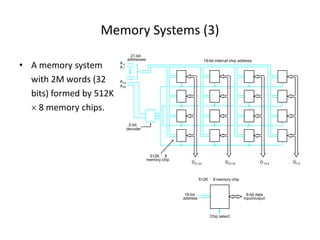
The document discusses various aspects of computer memory systems including main memory, cache memory, and memory mapping techniques. It provides details on:
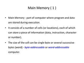
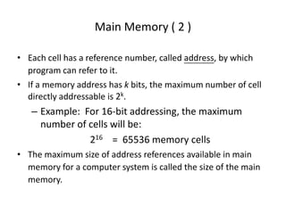
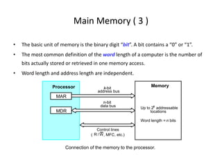
1) Main memory stores program and data during execution and consists of addressable memory cells. Memory access time is the time for a memory operation while cycle time is the minimum delay between operations.
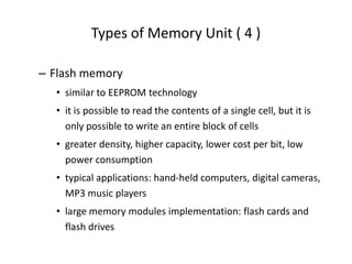
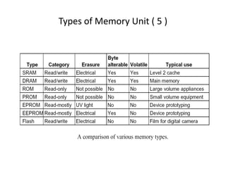
2) Memory units include RAM, ROM, PROM, EPROM, EEPROM and flash memory which have different characteristics like volatility and ability to be written.
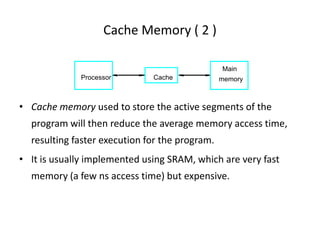
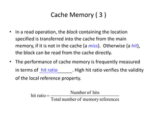
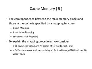
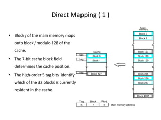
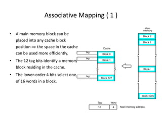
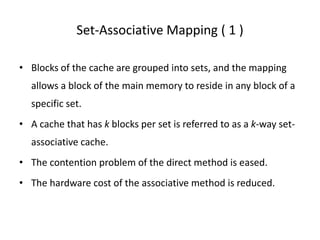
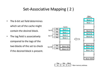
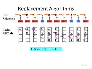
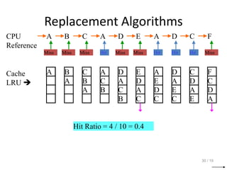
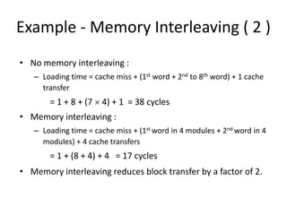
3) Cache memory uses fast SRAM to improve performance by taking advantage of locality of reference where nearby memory accesses are common. Mapping techniques like direct, associative and set-associative mapping determine how
Contents
• Main Memory
–Memory access time
– Memory cycle time
• Types of Memory Unit
– RAM
– ROM
• Memory System
• Cache Memory
– Associative mapping
– Direct mapping
– Set-associative mapping
– Replacement algorithm
• Memory Interleaving
2.
Main Memory (1 )
• Main Memory - part of computer where program and data
are stored during execution.
• It consists of a number of cells (or locations), each of which
can store a piece of information (data, instruction, character
or number).
• The size of the cell can be single byte or several successive
bytes (word) - byte-addressable or word-addressable
computer.
3.
Main Memory (2 )
• Each cell has a reference number, called address, by which
program can refer to it.
• If a memory address has k bits, the maximum number of cell
directly addressable is 2k.
– Example: For 16-bit addressing, the maximum
number of cells will be:
216 = 65536 memory cells
• The maximum size of address references available in main
memory for a computer system is called the size of the main
memory.
4.
Main Memory (3 )
• The basic unit of memory is the binary digit “bit”. A bit contains a “0” or “1”.
• The most common definition of the word length of a computer is the number of
bits actually stored or retrieved in one memory access.
• Word length and address length are independent.
Up to 2k
addressable
MDR
MAR
Connection of the memory to the processor.
k-bit
address bus
n-bit
data bus
Control lines
( , MFC, etc.)
Processor Memory
locations
Word length = n bits
W
R /
5.
Main Memory (4 )
• Memory Access Time
– The time that elapses between the initiation and the completion of
a memory access operation.
• e.g., the time between the READ and MFC signals
• Memory Cycle Time
– The minimum time delay required between two successive memory
access operations.
– The cycle time is usually slighter longer than the access time.
6.
Types of MemoryUnit ( 1 )
• Random-Access Memory (RAM)
– Any location can be accessed for a Read or Write
operation in some constant amount of time that is
independent of the memory location.
– Static RAM (SRAM)
• Memories that consist of circuits capable of retaining their state as long
as power is applied.
• SRAMs are fast (a few nanoseconds access time) but their cost is high.
– Dynamic RAM (DRAM)
• These memory units are capable of storing information for only tens of
milliseconds, thus require periodical refresh to maintain the contents.
7.
Types of MemoryUnit ( 2 )
• Read-Only Memory (ROM)
– Nonvolatile memory
– Data are written into a ROM when it is manufactured.
Normal operation involves only reading of stored data.
– ROM are useful as control store component in a
micro-programmed CPU (micro-coded CPU).
– ROM is also commonly used for storing the bootstrap
loader, a program whose function is to load the boot
program from the disk into the memory when the
power is turn on.
8.
Types of MemoryUnit ( 3 )
– PROM (Programmable ROM)
• data is allowed to be loaded by user but this process is
irreversible
• provide a faster and less expensive approach when
only a small number of data are required
– EPROM (Erasable, Programmable ROM)
• stored data can be erased by exposing the chip to
ultraviolet light and new data to be loaded
– EEPROM
• stored data can be erased electrically and selectively
• different voltages are needed for erasing, writing, and
reading the stored data
9.
Types of MemoryUnit ( 4 )
– Flash memory
• similar to EEPROM technology
• it is possible to read the contents of a single cell, but it is
only possible to write an entire block of cells
• greater density, higher capacity, lower cost per bit, low
power consumption
• typical applications: hand-held computers, digital cameras,
MP3 music players
• large memory modules implementation: flash cards and
flash drives
Memmory Systems (1)
•Implement a 64K X 8
memory using 16K X 1
memory chips
• Number of rows = 64K/16K =
4
• Number of columns =
8/1 = 8.
• 64K = 16 bit address.
• Each small chip needs 14 bit
(16K) address
• 16-14 = 2 bits for selecting
one of the four rows.
Data input
Chip select
memory chip
14-bit
address
16K X 8
Data output
12.
Memory Systems (2)
14-bitinternal chip address
decoder
2-bit
addresses
16-bit
A
0
A
1
A
1
4
memory chip
A1
5
16K 1
b7 b6 b0
Data i/p
Data o/p
X
13.
Memory Systems (3)
•A memory system
with 2M words (32
bits) formed by 512K
× 8 memory chips.
19-bit internal chip address
Chip select
memory chip
decoder
2-bit
addresses
21-bit
19-bit
address
512K 8
´
A 0
A 1
A19
memory chip
A20
D31-24 D7-0
D23-16 D15-8
512K 8
´
8-bit data
input/output
14.
Memory Systems (2 )
• Each chip has a control input called Chip Select (CS) used
to enable the chip.
• 21 address bits are needed to select a 32-bit word.
– The high-order 2 bits are decoded to determined which of the 4 CS
control signals are activated.
– The remaining 19 bits are used to access specific byte locations
inside each chip of the selected row.
15.
Memory Systems (3 )
• Single In-line Memory Modules (SIMMs) and
Dual In-line Memory Modules (DIMMs)
– An assembly of several memory chips on a
separate small board that plugs vertically into a
single socket on the motherboard.
– Occupy a smaller amount of space.
– Allow easy expansion.
16.
Cache Memory (1 )
• During the execution of a typical program it is often occurred
in a few localized areas of the program (in memory) at any
given interval of time –
• Locality of Reference
– temporal: a recently executed instructions is likely to be executed
again very soon, e.g., loop, stack.
– spatial: instructions in close proximity to a recently executed
instruction are also likely to be executed soon.
17.
Cache Memory (2 )
• Cache memory used to store the active segments of the
program will then reduce the average memory access time,
resulting faster execution for the program.
• It is usually implemented using SRAM, which are very fast
memory (a few ns access time) but expensive.
Cache
Main
memory
Processor
18.
Cache Memory (3 )
• In a read operation, the block containing the location
specified is transferred into the cache from the main
memory, if it is not in the cache (a miss). Otherwise (a hit),
the block can be read from the cache directly.
• The performance of cache memory is frequently measured
in terms of hit ratio . High hit ratio verifies the validity
of the local reference property.
references
memory
of
number
Total
hits
of
Number
ratio
hit =
19.
Cache Memory (4 )
• Two different ways of write access for system with cache
memory :
– (1) Write-through method – the cache and the main memory
locations are updated simultaneously.
– (2) Write-back method - cache location updated during a write
operation is marked with a dirty or modified bit. The main memory
location is updated later when the block is to be removed from the
cache.
20.
Cache Memory (5 )
• The correspondence between the main memory blocks and
those in the cache is specified by a mapping function.
– Direct Mapping
– Associative Mapping
– Set-associative Mapping
• To explain the mapping procedures, we consider
– a 2K cache consisting of 128 blocks of 16 words each, and
– a 64K main memory addressable by a 16-bit address, 4096 blocks of 16
words each.
21.
Direct Mapping (1 )
• Block j of the main memory maps
onto block j modulo 128 of the
cache.
• The 7-bit cache block field
determines the cache position.
• The high-order 5 tag bits identify
which of the 32 blocks is currently
resident in the cache.
tag
tag
tag
Cache
Main
memory
Block 0
Block 1
Block 127
Block 128
Block 129
Block 255
Block 256
Block 257
Block 4095
Block 0
Block 1
Block 127
7 4 Main memory address
Tag Block Word
5
22.
Direct Mapping (2 )
• Since more than one memory block is mapped
onto a given cache block position, contention
may arise for that position even when the
cache is not full.
• This technique is easy to implement, but it is
not flexible.
23.
Associative Mapping (1 )
• A main memory block can be
placed into any cache block
position ⇒ the space in the cache
can be used more efficiently.
• The 12 tag bits identify a memory
block residing in the cache.
• The lower-order 4 bits select one
of 16 words in a block.
4
tag
tag
tag
Cache
Main
memory
Block 0
Block 1
Blocki
Block 4095
Block 0
Block 1
Block 127
12 Main memory address
Tag Word
24.
Associative Mapping (2 )
• The cost of an associative cache is relatively
high because of the need to search all 128
tags to determine whether a given block is in
the cache.
• For performance reasons, associative search
must be done in parallel.
25.
Set-Associative Mapping (1 )
• Blocks of the cache are grouped into sets, and the mapping
allows a block of the main memory to reside in any block of a
specific set.
• A cache that has k blocks per set is referred to as a k-way set-
associative cache.
• The contention problem of the direct method is eased.
• The hardware cost of the associative method is reduced.
26.
Set-Associative Mapping (2 )
• The 6-bit set field determines
which set of the cache might
contain the desired block.
• The tag field is associatively
compared to the tags of the
two blocks of the set to check
if the desired block is present.
tag
tag
tag
Cache
Main
memory
Block 0
Block 1
Block 63
Block 64
Block 65
Block 127
Block 128
Block 129
Block 4095
Block 0
Block 1
Block 126
tag
tag
Block 2
Block 3
tag
Block 127
Main memory address
6 6 4
Tag Set Word
Set 0
Set 1
Set 63
27.
Replacement Algorithms
• Difficultto determine which blocks to kick out
• Least Recently Used (LRU) block
• The cache controller tracks references to all
blocks as computation proceeds.
• Increase / clear track counters when a hit/miss
occurs
28.
Replacement Algorithms
• ForAssociative & Set-Associative Cache
Which location should be emptied when the cache
is full and a miss occurs?
– First In First Out (FIFO)
– Least Recently Used (LRU)
• Distinguish an Empty location from a Full one
– Valid Bit
28 / 19
29.
Replacement Algorithms
29 /19
CPU
Reference
A B C A D E A D C F
Miss Miss Miss Hit Miss Miss Miss Hit Hit Miss
Cache
FIFO
A A
B
A
B
C
A
B
C
A
B
C
D
E
B
C
D
E
A
C
D
E
A
C
D
E
A
C
D
E
A
F
D
Hit Ratio = 3 / 10 = 0.3
30.
Replacement Algorithms
30 /19
CPU
Reference
A B C A D E A D C F
Miss Miss Miss Hit Miss Miss Hit Hit Hit Miss
Cache
LRU
A B
A
C
B
A
A
C
B
D
A
C
B
E
D
A
C
A
E
D
C
D
A
E
C
C
D
A
E
F
C
D
A
Hit Ratio = 4 / 10 = 0.4
31.
Memory Interleaving (1 )
• Main memory is structured as a number of physical modules (chip).
• Each memory module has its own Address Buffer Register (ABR) and Data
Buffer Register (DBR).
• Memory access may proceed in more than one module simultaneously →
the aggregate rate of transmission of words to and from the main
memory can be increased.
• How individual addresses are distributed over the modules is critical in
determining the average number of modules that can be kept busy.
32.
Memory Interleaving (2 )
• There are two memory address layouts :
(a) Consecutive words in a module
– The address consists of :
• (1) high-order k bits identify a single module (0 to n-1)
• (2) low-order m bits point to a particular word in that
module
• (3) Accessing consecutive addresses will keep
module busy.
33.
Memory Interleaving (3 )
(a) Consecutive words in a module
mbits
Address in module MM address
i
k bits
Module Module Module
Module
DBR
ABR DBR
ABR ABR DBR
0 n 1
-
34.
Memory Interleaving (4 )
(b) Consecutive words in consecutive modules
– The address consists of :
• (1) low-order k bits determine a module
• (2) high-order m bits name a location within that module
• (3) Accessing consecutive addresses will keep several
modules busy at any one time
– It is called Memory Interleaving.
– Faster access to a block of data.
– Higher average utilization of the memory system.
35.
Memory Interleaving (5 )
(b) Consecutive words in consecutive modules
i
k bits
0
Module
Module
Module
Module MM address
DBR
ABR
ABR DBR
ABR DBR
Address in module
2k
1
-
m bits
36.
Example - MemoryInterleaving ( 1 )
• Calculate the loading time difference between no memory
interleaving and 4-modules memory interleaving when a cache
read miss occurs where main memory have to be accessed and
subsequent transfer data to the cache.
– Size of block needed to transfer from memory to cache = 8 words
– Access time for main memory (1st word) = 8 cycles/word
– Access time for main memory (2nd to 8th word) = 4 cycles/word (No
address decoding is necessary for same memory module.)
– Access/transfer time from main memory to cache = 1 cycle/word
37.
Example - MemoryInterleaving ( 2 )
• No memory interleaving :
– Loading time = cache miss + (1st word + 2nd to 8th word) + 1 cache
transfer
= 1 + 8 + (7 × 4) + 1 = 38 cycles
• Memory interleaving :
– Loading time = cache miss + (1st word in 4 modules + 2nd word in 4
modules) + 4 cache transfers
= 1 + (8 + 4) + 4 = 17 cycles
• Memory interleaving reduces block transfer by a factor of 2.