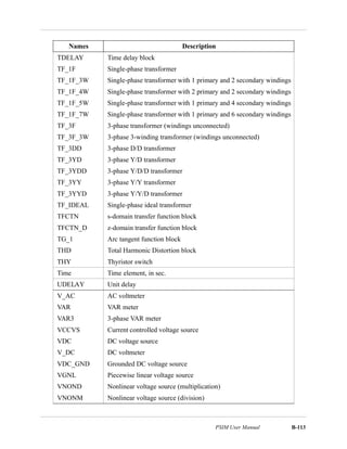
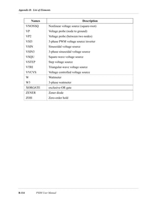
Downloaded 74 times


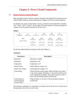
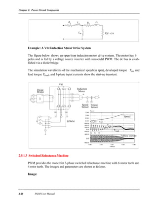
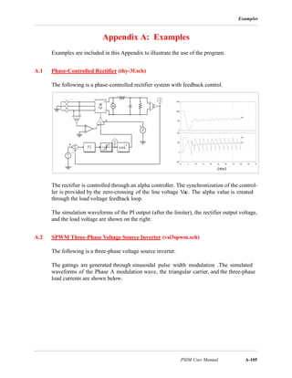
![Chapter 2: Power Circuit Component
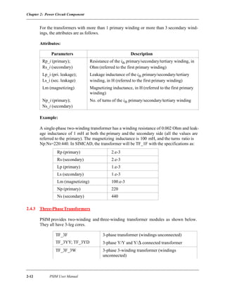
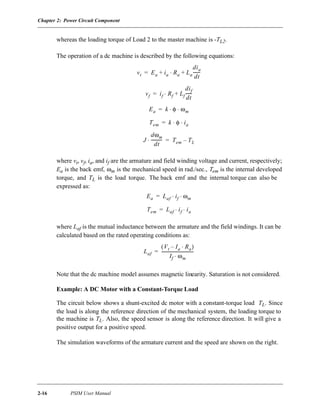
2-22 PSIM User Manual
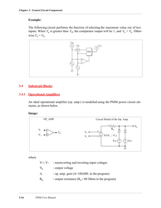
the following figure.
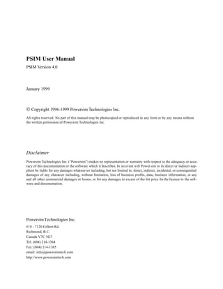
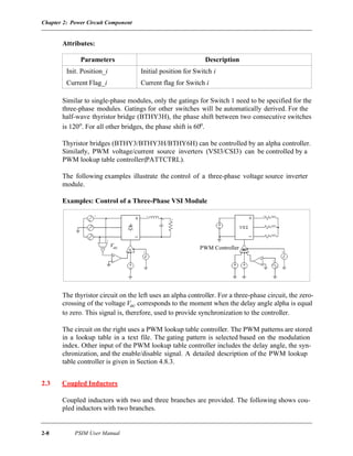
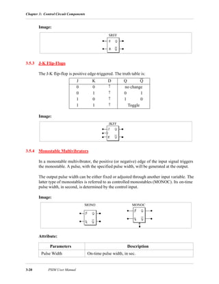
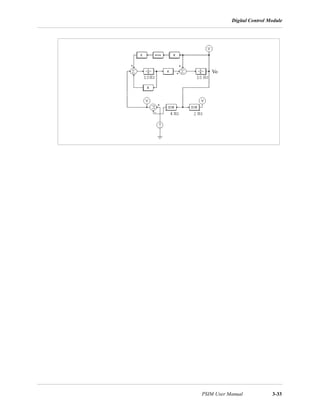
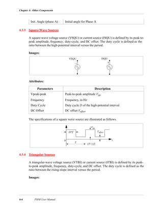
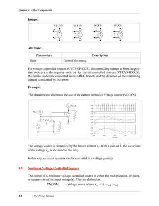
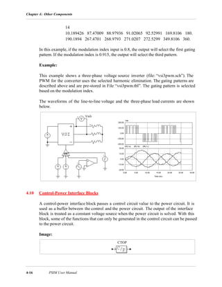
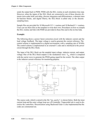
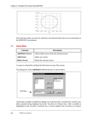
The rotor angle is defined such that, when the stator and the rotor teeth are completely out
of alignment, θ = 0. The value of the inductance can be in either rising stage, flat-top
stage, falling stage, or flat-bottom stage.
If we define the constant k as: , we can express the inductance L as a
function of the rotor angle θ:
L = Lmin + k ∗ θ [rising stage. Control signal c1=1)
L = Lmax [flat-top stage. Control signal c2=1)
L = Lmax - k ∗ θ [falling stage. Control signal c3=1)
L = Lmin [flat-bottom stage. Control signal c4=1)
The selection of the operating state is done through the control signal c 1, c2, c3, and c4
which are applied externally. For example, when c1 in Phase a is high (1), the rising stage
is selected and Phase a inductance will be: L = Lmin + k ∗ θ. Note that only one and at least
one control signal out of c1, c2, c3, and c4 in one phase must be high (1).
The developed torque of the machine per phase is:
Based on the inductance expression, we have the developed torque in each stage as:
Tem = i2
*k / 2 [rising stage]
Tem = 0 [flat-top stage]
θr
θ
Lmin
Lmax
L Rising Flat-Top Falling Flat-Bottom
k
Lmax Lmin–
θ
----------------------------=
Tem
1
2
--- i
2 dL
dθ
------⋅ ⋅=](https://image.slidesharecdn.com/manualpsim-150623050805-lva1-app6892/85/Manual-psim-34-320.jpg)
![Motor Drive Module
PSIM User Manual 2-23
Tem = - i2
*k / 2 [falling stage]
Tem = 0 [flat-bottom stage]
Note that saturation is not considered in this model.
2.5.2 Mechanical Loads
Several mechanical load models are provided in PSIM: constant-torque, constant-power,
and general-type load. Note that they are available in PSIM Plus only.
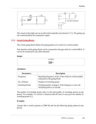
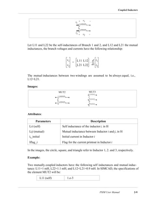
2.5.2.1 Constant-Torque Load
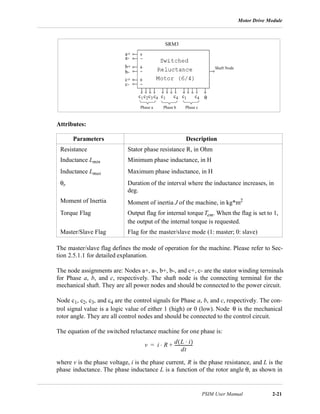
The image of a constant-torque load is:
Image:
Attributes:
If the reference direction of a mechanical system enters the dotted terminal, the load is
said to be along the reference direction, and the loading torque to the master machine is
Tconst. Otherwise the loading torque will be -Tconst. Please refer to Section2.5.1.1 for more
detailed explanation.
A constant-torque load is expressed as:
The torque does not depend on the speed direction.
Parameters Description
Constant Torque Torque constant Tconst, in N*m
Moment of Inertia Moment of inertia of the load, in kg*m2
MLOAD_T
TL Tconst=](https://image.slidesharecdn.com/manualpsim-150623050805-lva1-app6892/85/Manual-psim-35-320.jpg)


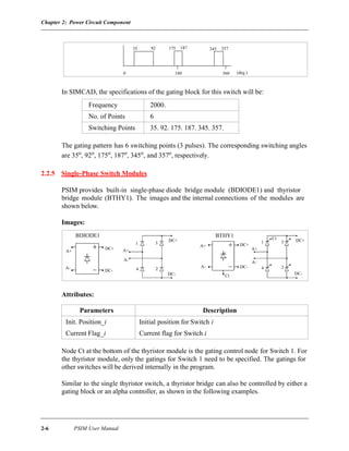
![Chapter 3: Control Circuit Components
3-6 PSIM User Manual
Attributes:
For SUM3, the input with a dot is the first input.
If the inputs are scalar, the output of a sumer with n inputs is defined as:
If the input is a vector, the output of a two-input summer will also be a vector, which is
defined as:
V1 = [a1 a2 ... an]
V2 = [b1 b2 ... bn]
Vo = V1 + V2 = [a1+b1 a2+b2 ... an+bn]
For a one-input sumer, the output will still be a scalar which is equal to the summation of
the input vector elements, that is, Vo = a1 + a2 + ... an.
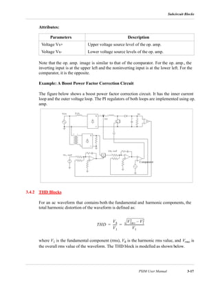
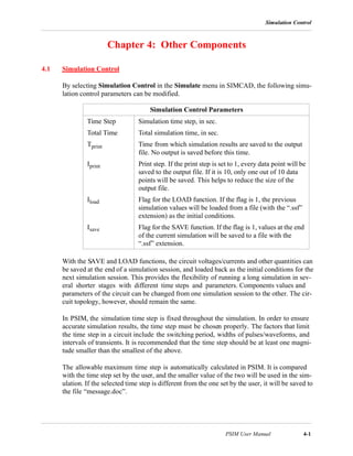
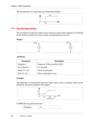
3.2.2 Multipliers and Dividers
The output of a multipliers (MULT) or dividers (DIVD) is equal to the multiplication or
division of two input signals.
Images:
For the divider, the dotted node is for the nominator input.
The input of a multiplier can be either a vector or a scalar. If the two inputs are vectors,
their dimensions must be equal. Let the two inputs be:
V1 = [a1 a2 ... an]
V2 = [b1 b2 ... bn]
The output, which is a scalar, will be:
Parameters Description
Gain_i Gain ki for the ith input
Vo k1V1 k2V2 ... knVn+ + +=
MULT DIVD
Nominator
Denominator](https://image.slidesharecdn.com/manualpsim-150623050805-lva1-app6892/85/Manual-psim-44-320.jpg)

![Digital Control Module
PSIM User Manual 3-23
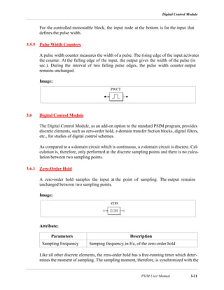
If a0 = 1, the expression Y(z) = H(z) * U(z) can be expressed in difference equation as:
Image:
Attributes:
Example:
The following is a second-order transfer function:
with a sampling frequency of 3 kHz. In SIMCAD, the specifications are:
3.6.2.1 Integrators
There are two types of integrators. One is the regular integrator (I_D). The other is the
Parameters Description
Order N Order N of the transfer function
Coeff. b0...bN Coefficients of the nominator (from b0 to bN)
Coeff. a0...aN Coefficients of the nominator (from a0 to aN)
Sampling Frequency Sampling frequency, in Hz
Order N 2
Coeff. b0...bN 0. 0. 400.e3
Coeff. a0...aN 1. 1200. 400.e3
Sampling Frequency 3000.
H z( )
b0 z
N
b1 z
N 1–
⋅ ... bN 1– z bN+⋅+ + +⋅
a0 z
N
a1 z
N 1–
⋅ ... aN 1– z aN+⋅+ + +⋅
---------------------------------------------------------------------------------------------=
y n( ) b0 u n( ) b1 u n 1–( )⋅ ... bN u n N–( ) –⋅+ + +⋅=
a1 y n 1–( )⋅ a2 y n 2–( )⋅ ... aN y n N–( )⋅+ + +[ ]
TFCTN_D
H z( )
400.e
3
z
2
1200 z 400.e
3
+⋅+
----------------------------------------------------=](https://image.slidesharecdn.com/manualpsim-150623050805-lva1-app6892/85/Manual-psim-61-320.jpg)
![Chapter 3: Control Circuit Components
3-26 PSIM User Manual
If the denominator coefficients a0..aN are not zero, this type of filter is called infinite
impulse response (IIR) filter.
The transfer function of the FIR filter is expressed in polynomial form as:
If a0 = 1, the output y and input u can be expressed in difference equation form as:
Filter coefficients can be specified either directly or through a file. The following are the
filter images and attributes when filter coefficients are specified directly.
Images:
Attributes:
The following are the filter images and attributes when filter coefficients are specified
through a file.
Images:
Parameters Description
Order N Order N of the transfer function
Coeff. b0...bN Coefficients of the nominator (from b0 to bN)
Coeff. a0...aN Coefficients of the nominator (from a0 to aN)
Sampling Frequency Sampling frequency, in Hz
y n( ) b0 u n( ) b1 u n 1–( )⋅ ... bN u n N–( ) –⋅+ + +⋅=
a1 y n 1–( )⋅ a2 y n 2–( )⋅ ... aN y n N–( )⋅+ + +[ ]
H z( ) b0 b1 z
1–
⋅ ... bN 1– z
N 1–( )–
bN z
N–
⋅+⋅+ + +=
y n( ) b0 u n( ) b1 u n 1–( )⋅ ... bN u n N–( )⋅+ + +⋅=
FILTER_FIRFILTER_D
FILTER_FIR1FILTER_D1](https://image.slidesharecdn.com/manualpsim-150623050805-lva1-app6892/85/Manual-psim-64-320.jpg)
![Digital Control Module
PSIM User Manual 3-27
Attributes:
The coefficient file has the following format:
Example:
To design a 2nd-order low-pass Butterworth digital filter with the cut-off frequency fc = 1
kHz, assuming the sampling frequency fs = 10 kHz, usingMATLAB *, we have:
Nyquist frequency fn = fs / 2 = 5 kHz
Normalized cut-off frequency fc* = fc/fn = 1/5 = 0.2
[B,A] = butter (2, fc*)
which will give:
B = [0.0201 0.0402 0.0201 ] = [b0 b1 b2]
A = [ 1 -1.561 0.6414 ] = [a0 a1 a2]
The transfer function is:
The input-output difference equation is:
The parameter specification of the filter in SIMCAD will be:
Parameters Description
File for Coefficients Name of the file storing the filter coefficients
Sampling Frequency Sampling frequency, in Hz
For FILTER_D1 For FILTER_FIR1
N
b0, a0
b1, a1
... ... ...
bN, aN
N
b0
b1
... ... ...
bN
*. MATLAB is a registered trademark of MathWorks, Inc.
H z( )
0.0201 0.0402 z
1–
⋅ 0.0201 z
2–
⋅+ +
1 1.561– z
1–
⋅ 0.6414 z
2–
⋅+
-------------------------------------------------------------------------------------=
y n( ) 0.0201 u n( ) 0.0402 u n 1–( )⋅ 1.561 y n 1–( )⋅ 0.6414– y n 2–( )⋅+ +⋅=](https://image.slidesharecdn.com/manualpsim-150623050805-lva1-app6892/85/Manual-psim-65-320.jpg)
![Digital Control Module
PSIM User Manual 3-31
Image:
Let the two input vectors be:
A = [ am am-1 am-2 ... a1]
B = [ bn bn-1 bn-2 ... b1]
We have the convolution of A and B as:
= [cm+n-1 cm+n-2 ... c1]
where
ci = Σ [ ak+1 * bj-k], k=0, ..., m+n-1; j=0, ..., m+n-1; i=1, ..., m+n-1
Example:
If A = [1 2 3] and B = [4 5], we have m = 3; n = 2; and the convolution of A and B as C =
[4 13 22 15].
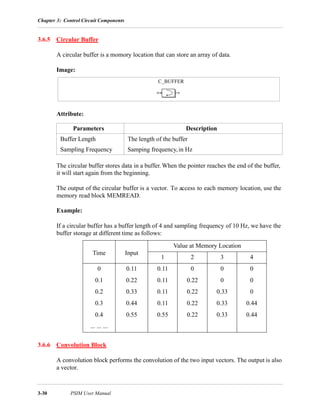
3.6.7 Memory Read Block
A memory read block can be used to read the value of a memory location ofa vector.
Image:
Attribute:
This block allows one to access the memory location of elements, such as the convolution
block, vector array, and circular buffer. The index offset defines the offset from the start-
ing memory location.
Parameters Description
Memory Index Offset Offset from the starting memory location
CONV
C A B⊗=
MEMREAD](https://image.slidesharecdn.com/manualpsim-150623050805-lva1-app6892/85/Manual-psim-69-320.jpg)
![Chapter 3: Control Circuit Components
3-32 PSIM User Manual
Example:
Let a vector be A = [2 4 6 8], if index offset is 0, the memory read block output is 2. If the
index offset is 2, the output is 6.
3.6.8 Data Array
This is a one-dimensional array. The output is a vector.
Image:
Attribute:
Example:
To define an array A = [2 4 6 8], we will have: Array Length = 4; Values = 2 4 6 8.
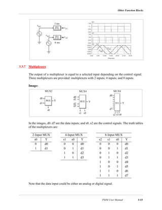
3.6.9 Multi-Rate Sampling System
A discrete system can have more than one different sampling rate. The following system is
used to illustrate this.
The system below has 3 sections. The first section has a sampling rate of 10 Hz. The out-
put, Vo, fed back to the system and is sampled at 4 Hz in the second section. In the third
section, the output is displayed at a sampling rate of 2 Hz.
It should be noted that a zero-order hold must be used between two elements having dif-
ferent sampling rates.
Parameters Description
Array Length The length of the data array
Values Values of the array
ARRAY](https://image.slidesharecdn.com/manualpsim-150623050805-lva1-app6892/85/Manual-psim-70-320.jpg)

![External DLL Blocks
PSIM User Manual 4-21
// This is a sample C program for Microsoft C/C++ which is to be linked to PSIM via DLL.
// To compile it into DLL:
// From the command window, run the command "cl /LD ms_user4.c"
// From Miscrosoft Developer Studio:
// - From the "File" menu, choose "New"/"Project Workspace", and select "Dynamic-Link Library".
// Set the name as "ms_user4".
// - Copy this sample file into the directory where the project resides.
// - From the "Insert" menu, choose "Files into Project", and select "ms_user4.c".
// - Choose active configuration to "Release". From the "Build" menu, choose "Rebuild All".
// After the DLL file "ms_user4.dll" is generated, backup the default file into another file or directory,
// and copy your DLL file into the PSIM directory (and overwriting the existing file). You are then ready
// to run PSIM with your DLL.
// This sample program implement the control of the circuit "pfvi-dll.sch" in a C routine.
// Input: in[0]=Vin; in[1]=iL; in[2]=Vo
// Output: Vm=out[0]; iref=out[1]
// Do not change the following line. It’s for DLL
__declspec(dllexport)
// You may change the variable names (say from "t" to "Time").
// But DO NOT change the function name, number of variables, variable type, and sequence.
// Variables:
// t: Time, passed from PSIM by value
// delt: Time step, passed from PSIM by value
// in: input array, passed from PSIM by reference
// out: output array, sent back to PSIM (Note: the values of out[*] can be modified in PSIM)
// The maximum length of the input and output array "in" and "out" is 20.
// Warning: Global variables above the function ms_user4 (t,delt,in,out) are not allowed!!!
void ms_user4 (t, delt, in, out)
// Note that all the variables must be defined as "double"
double t, delt;
double *in, *out;
{
// Place your code here............begin
doubleVoref=10.5, Va, iref, iL, Vo, Vm;
double errv, erri, Ts=33.33e-6;
static double yv=0., yi=0., uv=0., ui=0.;
// Input
Va=fabs(in[0]);
iL=in[1];
Vo=in[2];
// Outer Loop
errv=Voref-Vo;
// Trapezoidal Rule
yv=yv+(33.33*errv+uv)*Ts/2.;](https://image.slidesharecdn.com/manualpsim-150623050805-lva1-app6892/85/Manual-psim-93-320.jpg)
![Chapter 4: Other Components
4-22 PSIM User Manual
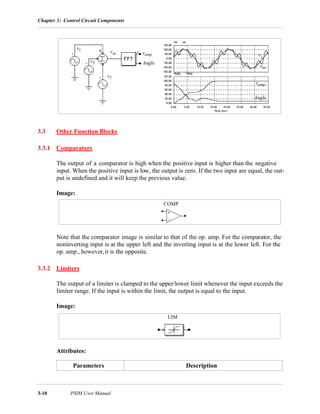
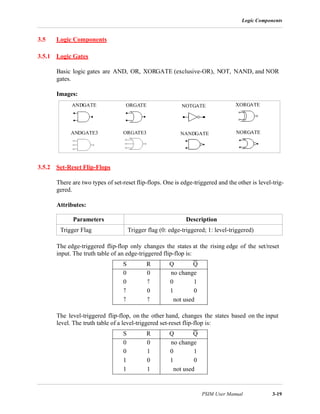
4.13 Simulated Frequency Response Analyzers
Similar to the actual frequency response analyzer, the Simulated Frequency Response
Analyzer (SFRA) measures the frequency response of a system between the input and the
output. The input of the analyzer must be connected to a sinusoidal source. The response,
measured in dB for the amplitude and in degrees for the phase angle, is calculated at the
end of the simulation and is stored in a file with the “.fre” extension.
Image:
The current version of SFRA only calculates the frequency response at one point. T
obtain the frequency response over a frequency region, one needs to manually change the
excitation frequency for different values.
In order to obtain accurate results, one should make sure that the output reaches the steady
state at the end of the simulation. Moreover, the amplitude of the sinusoidal excitation
source needs to be properly selected to maintain the small-signal linearity of the system.
// Backward Euler
// yv=yv+33.33*errv*Ts;
iref=(errv+yv)*Va;
// Inner Loop
erri=iref-iL;
// Trapezoidal Rule
yi=yi+(4761.9*erri+ui)*Ts/2.;
// Backward Euler
// yi=yi+4761.9*erri*Ts;
Vm=yi+0.4*erri;
// Store old values
uv=33.33*errv;
ui=4761.9*erri;
// Output
out[0]=Vm;
out[1]=iref;
// Place your code here............end
}
SFRA
OutputInput](https://image.slidesharecdn.com/manualpsim-150623050805-lva1-app6892/85/Manual-psim-94-320.jpg)


Diodes conduct current only when forward biased and block current when reverse biased, while zener diodes act as normal diodes during forward bias but regulate voltage during reverse bias by allowing current to flow at the zener voltage. Both components are ideal switches with micro-ohm on resistance and mega-ohm off resistance and do not require modeling of turn-on and turn-off transients.