Kannan M 
Mobile: +91-8105233771 Email: m_kannan11@yahoo.in 
Experience Summary: 
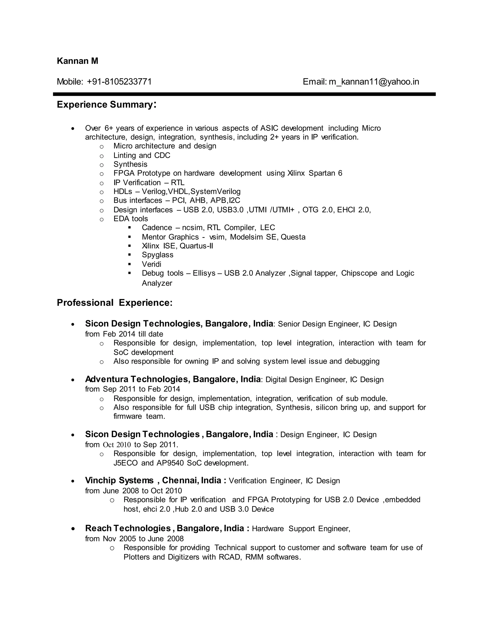
ď‚· Over 6+ years of experience in various aspects of ASIC development including Micro 
architecture, design, integration, synthesis, including 2+ years in IP verification. 
o Micro architecture and design 
o Linting and CDC 
o Synthesis 
o FPGA Prototype on hardware development using Xilinx Spartan 6 
o IP Verification – RTL 
o HDLs – Verilog,VHDL,SystemVerilog 
o Bus interfaces – PCI, AHB, APB,I2C 
o Design interfaces – USB 2.0, USB3.0 ,UTMI /UTMI+ , OTG 2.0, EHCI 2.0, 
o EDA tools 
 Cadence – ncsim, RTL Compiler, LEC 
ď‚§ Mentor Graphics - vsim, Modelsim SE, Questa 
ď‚§ Xilinx ISE, Quartus-II 
ď‚§ Spyglass 
ď‚§ Veridi 
 Debug tools – Ellisys – USB 2.0 Analyzer ,Signal tapper, Chipscope and Logic 
Analyzer 
Professional Experience: 
ď‚· Sicon Design Technologies, Bangalore, India: Senior Design Engineer, IC Design 
from Feb 2014 till date 
o Responsible for design, implementation, top level integration, interaction with team for 
SoC development 
o Also responsible for owning IP and solving system level issue and debugging 
ď‚· Adventura Technologies, Bangalore, India: Digital Design Engineer, IC Design 
from Sep 2011 to Feb 2014 
o Responsible for design, implementation, integration, verification of sub module. 
o Also responsible for full USB chip integration, Synthesis, silicon bring up, and support for 
firmware team. 
ď‚· Sicon Design Technologies , Bangalore, India : Design Engineer, IC Design 
from Oct 2010 to Sep 2011. 
o Responsible for design, implementation, top level integration, interaction with team for 
J5ECO and AP9540 SoC development. 
ď‚· Vinchip Systems , Chennai, India : Verification Engineer, IC Design 
from June 2008 to Oct 2010 
o Responsible for IP verification and FPGA Prototyping for USB 2.0 Device ,embedded 
host, ehci 2.0 ,Hub 2.0 and USB 3.0 Device 
ď‚· Reach Technologies , Bangalore, India : Hardware Support Engineer, 
from Nov 2005 to June 2008 
o Responsible for providing Technical support to customer and software team for use of 
Plotters and Digitizers with RCAD, RMM softwares.
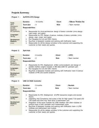
Projects Summary: 
Project 1 : ALPOTG OTG Design 
Tools: 
Verdi, 
Questasim, 
NCSIM, 
Spyglass, 
RC-synthesis, 
Languages: 
Verilog, 
Development 
Platform: 
Linux 
Duration : 10 months Client : Silicon Motion Inc 
Team size : 4 Role : Team member 
Responsibilities: 
ď‚· Responsible for micro-architecture design of device controller (mmu design, 
cepc,ncepc, and uppie). 
ď‚· Responsible for RTL Design of various modules of device controller (mmu 
design, cepc, ncepc, and uppie). 
ď‚· Run Spyglass for Lint and CDC checks. 
ď‚· Bug fixes of designed modules and working with Verification team. 
ď‚· Responsible for all the release activities to the customer and supporting the 
customer on their needs and queries. 
Project 2 : Split Hub 
Tools: 
Verdi 
Questasim, 
NCSIM, 
Spyglass, 
RC-synthesis, 
Languages: 
Verilog, 
Development 
Platform: 
Linux 
Duration : 6 months Client : AMS 
Team size : 2 Role : Team member 
Responsibilities: 
ď‚· Responsible for RTL Development of 8bit control endpoint and design of 
parallel interface engine modules in 8bit data width for upstream part. 
ď‚· Run Spyglass for Lint and CDC checks 
ď‚· Bug fixes of designed modules and working with Verification team In various 
modules of PIE and Control endpoint. 
Project 3 : USB 2.0 HUB Controller 
Tools: 
Questasim, 
NCSIM, 
Spyglass, 
RC-synthesis, 
Languages: 
Verilog, 
Development 
Platform: 
Linux 
Duration : 6 months Client : Realtek 
Team size : 3 Role : Team member 
Responsibilities: 
ď‚· Responsible for RTL Development of LPM transaction engine and receiver 
blocks. 
ď‚· Upgrading Hub Compliance test suites in Hub for High speed, Full speed and 
Low speed and done bug fixes done in downstream port. 
ď‚· Integration of the reuse modules for UTMI Interface with other modules on 
protocol layer in both upstream and 4 downstream ports. 
ď‚· Bug fixes of designed modules and working with Verification team in LPM 
modules and downstream port module. 
ď‚· Responsible for all the release activities to the customer and supporting the 
customer on their needs and queries.
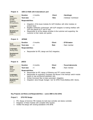
Project 4: USB 2.0 HUB with 4 downstream port 
Tools: 
Questasim, 
NCSIM, 
Spyglass, 
RC-synthesis, 
Languages: 
Verilog, 
Development 
Platform: 
Linux 
Duration : 2 months Client : Quicklogic 
Team size : 1 Role : Individual Contributor 
Responsibilities: 
ď‚· Integration of the reuse modules for ULPI Interface with other modules on 
protocol layer. 
ď‚· Modified Verification environment with ULPI wrappers to making interface with 
ULPI and placed at 2nd and 3rd port. 
ď‚· Responsible for all the release activities to the customer and supporting the 
customer on their needs and queries. 
Project 5: AP9540 
Tools: 
Questasim,Verdi 
Languages: 
Verilog,VHDL 
Development 
Platform: 
Linux 
Duration : 5 months Client : ST-Ericssion 
Team size : 4 Role : Team member 
Responsibilities: 
ď‚· Responsible for RTL design and SoC integration. 
Project 6: J5ECO 
Tools: 
Verdi 
Autogen 
ncsim 
Languages: 
Verilog,VHDL 
Development 
Platform: 
Linux 
Duration : 6 months Client : Texas Instruments 
Team size : 4 Role : Team member 
Responsibilities: 
ď‚· Responsible for RTL design of Dithering and TFT control module 
ď‚· Responsible for expanding Crossbars and Muxes in the interrupt switch module 
based on new architecture peripheral sets. 
ď‚· Written Command files to make automated integration. 
ď‚· Integration done through Autogen tool for GPIO,Timers,Mailbox,ADC blocks. 
Key Projects and Roles and Responsibilities :- (June 2008 to Oct 2010) 
Project 1: OTG PIE Design 
ď‚· RTL Design of Common PIE modules for both host controller and device controller. 
ď‚· Integration of these modules with complete OTG System. 
ď‚· Verified this design with existing standalone OTG BFM.
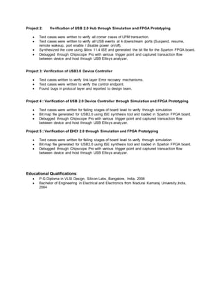
Project 2: Verification of USB 2.0 Hub through Simulation and FPGA Prototyping 
ď‚· Test cases were written to verify all corner cases of LPM transaction. 
ď‚· Test cases were written to verify all USB events at 4 downstream ports (Suspend, resume, 
remote wakeup, port enable / disable power on/off). 
ď‚· Synthesized the core using Xilinx 11.4 ISE and generated the bit file for the Sparton FPGA board. 
ď‚· Debugged through Chipscope Pro with various trigger point and captured transaction flow 
between device and host through USB Ellisys analyzer. 
Project 3: Verification of USB3.0 Device Controller 
ď‚· Test cases written to verify link layer Error recovery mechanisms. 
ď‚· Test cases were written to verify the control endpoint. 
ď‚· Found bugs in protocol layer and reported to design team. 
Project 4 : Verification of USB 2.0 Device Controller through Simulation and FPGA Prototyping 
ď‚· Test cases were written for failing stages of board level to verify through simulation 
ď‚· Bit map file generated for USB2.0 using ISE synthesis tool and loaded in Sparton FPGA board. 
ď‚· Debugged through Chipscope Pro with various trigger point and captured transaction flow 
between device and host through USB Ellisys analyzer. 
Project 5 : Verification of EHCI 2.0 through Simulation and FPGA Prototyping 
ď‚· Test cases were written for failing stages of board level to verify through simulation 
ď‚· Bit map file generated for USB2.0 using ISE synthesis tool and loaded in Sparton FPGA board. 
ď‚· Debugged through Chipscope Pro with various trigger point and captured transaction flow 
between device and host through USB Ellisys analyzer. 
Educational Qualifications: 
ď‚· P.G Diploma in VLSI Design, Silicon Labs, Bangalore, India, 2008 
ď‚· Bachelor of Engineering in Electrical and Electronics from Madurai Kamaraj University,India, 
2004

Kannan_Resume

  • 1.
    Kannan M Mobile:+91-8105233771 Email: m_kannan11@yahoo.in Experience Summary:  Over 6+ years of experience in various aspects of ASIC development including Micro architecture, design, integration, synthesis, including 2+ years in IP verification. o Micro architecture and design o Linting and CDC o Synthesis o FPGA Prototype on hardware development using Xilinx Spartan 6 o IP Verification – RTL o HDLs – Verilog,VHDL,SystemVerilog o Bus interfaces – PCI, AHB, APB,I2C o Design interfaces – USB 2.0, USB3.0 ,UTMI /UTMI+ , OTG 2.0, EHCI 2.0, o EDA tools  Cadence – ncsim, RTL Compiler, LEC  Mentor Graphics - vsim, Modelsim SE, Questa  Xilinx ISE, Quartus-II  Spyglass  Veridi  Debug tools – Ellisys – USB 2.0 Analyzer ,Signal tapper, Chipscope and Logic Analyzer Professional Experience:  Sicon Design Technologies, Bangalore, India: Senior Design Engineer, IC Design from Feb 2014 till date o Responsible for design, implementation, top level integration, interaction with team for SoC development o Also responsible for owning IP and solving system level issue and debugging  Adventura Technologies, Bangalore, India: Digital Design Engineer, IC Design from Sep 2011 to Feb 2014 o Responsible for design, implementation, integration, verification of sub module. o Also responsible for full USB chip integration, Synthesis, silicon bring up, and support for firmware team.  Sicon Design Technologies , Bangalore, India : Design Engineer, IC Design from Oct 2010 to Sep 2011. o Responsible for design, implementation, top level integration, interaction with team for J5ECO and AP9540 SoC development.  Vinchip Systems , Chennai, India : Verification Engineer, IC Design from June 2008 to Oct 2010 o Responsible for IP verification and FPGA Prototyping for USB 2.0 Device ,embedded host, ehci 2.0 ,Hub 2.0 and USB 3.0 Device  Reach Technologies , Bangalore, India : Hardware Support Engineer, from Nov 2005 to June 2008 o Responsible for providing Technical support to customer and software team for use of Plotters and Digitizers with RCAD, RMM softwares.
  • 2.
    Projects Summary: Project1 : ALPOTG OTG Design Tools: Verdi, Questasim, NCSIM, Spyglass, RC-synthesis, Languages: Verilog, Development Platform: Linux Duration : 10 months Client : Silicon Motion Inc Team size : 4 Role : Team member Responsibilities: ď‚· Responsible for micro-architecture design of device controller (mmu design, cepc,ncepc, and uppie). ď‚· Responsible for RTL Design of various modules of device controller (mmu design, cepc, ncepc, and uppie). ď‚· Run Spyglass for Lint and CDC checks. ď‚· Bug fixes of designed modules and working with Verification team. ď‚· Responsible for all the release activities to the customer and supporting the customer on their needs and queries. Project 2 : Split Hub Tools: Verdi Questasim, NCSIM, Spyglass, RC-synthesis, Languages: Verilog, Development Platform: Linux Duration : 6 months Client : AMS Team size : 2 Role : Team member Responsibilities: ď‚· Responsible for RTL Development of 8bit control endpoint and design of parallel interface engine modules in 8bit data width for upstream part. ď‚· Run Spyglass for Lint and CDC checks ď‚· Bug fixes of designed modules and working with Verification team In various modules of PIE and Control endpoint. Project 3 : USB 2.0 HUB Controller Tools: Questasim, NCSIM, Spyglass, RC-synthesis, Languages: Verilog, Development Platform: Linux Duration : 6 months Client : Realtek Team size : 3 Role : Team member Responsibilities: ď‚· Responsible for RTL Development of LPM transaction engine and receiver blocks. ď‚· Upgrading Hub Compliance test suites in Hub for High speed, Full speed and Low speed and done bug fixes done in downstream port. ď‚· Integration of the reuse modules for UTMI Interface with other modules on protocol layer in both upstream and 4 downstream ports. ď‚· Bug fixes of designed modules and working with Verification team in LPM modules and downstream port module. ď‚· Responsible for all the release activities to the customer and supporting the customer on their needs and queries.
  • 3.
    Project 4: USB2.0 HUB with 4 downstream port Tools: Questasim, NCSIM, Spyglass, RC-synthesis, Languages: Verilog, Development Platform: Linux Duration : 2 months Client : Quicklogic Team size : 1 Role : Individual Contributor Responsibilities: ď‚· Integration of the reuse modules for ULPI Interface with other modules on protocol layer. ď‚· Modified Verification environment with ULPI wrappers to making interface with ULPI and placed at 2nd and 3rd port. ď‚· Responsible for all the release activities to the customer and supporting the customer on their needs and queries. Project 5: AP9540 Tools: Questasim,Verdi Languages: Verilog,VHDL Development Platform: Linux Duration : 5 months Client : ST-Ericssion Team size : 4 Role : Team member Responsibilities: ď‚· Responsible for RTL design and SoC integration. Project 6: J5ECO Tools: Verdi Autogen ncsim Languages: Verilog,VHDL Development Platform: Linux Duration : 6 months Client : Texas Instruments Team size : 4 Role : Team member Responsibilities: ď‚· Responsible for RTL design of Dithering and TFT control module ď‚· Responsible for expanding Crossbars and Muxes in the interrupt switch module based on new architecture peripheral sets. ď‚· Written Command files to make automated integration. ď‚· Integration done through Autogen tool for GPIO,Timers,Mailbox,ADC blocks. Key Projects and Roles and Responsibilities :- (June 2008 to Oct 2010) Project 1: OTG PIE Design ď‚· RTL Design of Common PIE modules for both host controller and device controller. ď‚· Integration of these modules with complete OTG System. ď‚· Verified this design with existing standalone OTG BFM.
  • 4.
    Project 2: Verificationof USB 2.0 Hub through Simulation and FPGA Prototyping ď‚· Test cases were written to verify all corner cases of LPM transaction. ď‚· Test cases were written to verify all USB events at 4 downstream ports (Suspend, resume, remote wakeup, port enable / disable power on/off). ď‚· Synthesized the core using Xilinx 11.4 ISE and generated the bit file for the Sparton FPGA board. ď‚· Debugged through Chipscope Pro with various trigger point and captured transaction flow between device and host through USB Ellisys analyzer. Project 3: Verification of USB3.0 Device Controller ď‚· Test cases written to verify link layer Error recovery mechanisms. ď‚· Test cases were written to verify the control endpoint. ď‚· Found bugs in protocol layer and reported to design team. Project 4 : Verification of USB 2.0 Device Controller through Simulation and FPGA Prototyping ď‚· Test cases were written for failing stages of board level to verify through simulation ď‚· Bit map file generated for USB2.0 using ISE synthesis tool and loaded in Sparton FPGA board. ď‚· Debugged through Chipscope Pro with various trigger point and captured transaction flow between device and host through USB Ellisys analyzer. Project 5 : Verification of EHCI 2.0 through Simulation and FPGA Prototyping ď‚· Test cases were written for failing stages of board level to verify through simulation ď‚· Bit map file generated for USB2.0 using ISE synthesis tool and loaded in Sparton FPGA board. ď‚· Debugged through Chipscope Pro with various trigger point and captured transaction flow between device and host through USB Ellisys analyzer. Educational Qualifications: ď‚· P.G Diploma in VLSI Design, Silicon Labs, Bangalore, India, 2008 ď‚· Bachelor of Engineering in Electrical and Electronics from Madurai Kamaraj University,India, 2004