Download as PDF, PPTX
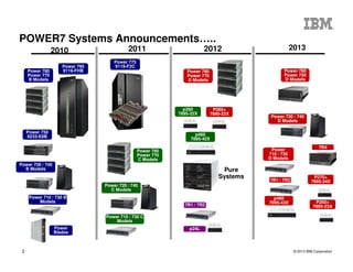
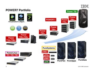
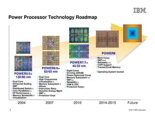
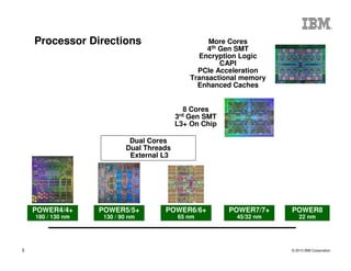
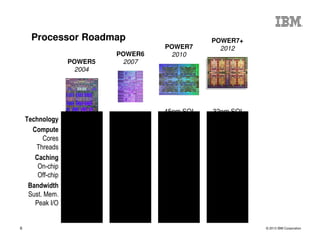
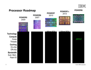
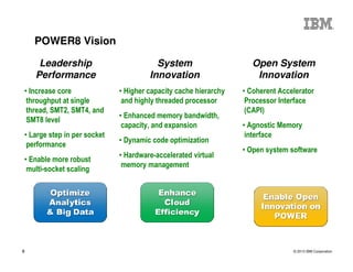
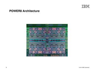


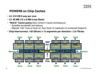


The document outlines the development and features of IBM's Power processors, specifically the Power8 architecture, highlighting improved core throughput, caching structures, and memory bandwidth. It details advancements such as transactional memory support, integrated PCIe Gen3, and higher performance across multiple sockets. Additionally, it discusses the roadmap from previous generations, showcasing the evolution in technology from Power5 through Power8.